OPTOELECTRONIC AND THERMAL
PROPERTIES OF METALLIC TRANSITION
METAL DICHALCOGENIDES
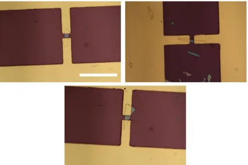
a dissertation submitted to
the graduate school of engineering and science
of bilkent university
in partial fulfillment of the requirements for
the degree of
doctor of philosophy
in
materials science and nanotechnology
By
Naveed Mehmood
November 2020
Optoelectronic and Thermal Properties of Metallic Transition Metal Dichalcogenides
By Naveed Mehmood November 2020
We certify that we have read this dissertation and that in our opinion it is fully adequate, in scope and in quality, as a dissertation for the degree of Doctor of Philosophy.
Talip Serkan Kasırga(Advisor)
Menderes I¸skin
Selim Hanay
Hilmi Volkan Demir
Hasan S¸ahin
Approved for the Graduate School of Engineering and Science:
Ezhan Kara¸san
ABSTRACT
OPTOELECTRONIC AND THERMAL PROPERTIES
OF METALLIC TRANSITION METAL
DICHALCOGENIDES
Naveed Mehmood
Ph.D. in Materials Science and Nanotechnology Advisor: Talip Serkan Kasırga
November 2020
After the successful isolation of graphene monolayer from its bulky counterpart, there has been tremendous advancement in the field of 2D material. Transi-tion metal dichalcogenides(TMDCs) is family of 2D materials comprising of a transition metal atom sandwiched between two chalcogen atoms. Photoresponse of semiconducting TMDCs has been studied extensively in literature. However, photoresponse from metallic TMDCs is unprecedented and hence has not been studied to explore which mechanism might prevail. Among our findings, we dis-covered that photocurrent generation through metallic TMDCs is possible and has a photo-thermal origin. Using scanning photo-current microscopy, we were able to obtain spatial photocurrent maps for both, zero biased and biased sam-ples. At zero applied bias, the photocurrent generation is localized to metal-metal junction and governed by Seebeck effect. At finite applied bias, photocurrent from the whole crystal is observed and is due to photobolometric effect. As Photo-bolometric effect relies on photo-thermally induced resistance change of the material, we extended our study to extract thermal conductivity of metal-lic TMDCs via bolometric effect. As contact of crystal with substrate act as a heat sink, we used suspended crystals over a hole to thermally isolate it from any heat sink. Resistance change via laser induced heating is experimentally measured at the center of the suspended part of crystal. Measured resistance change is matched with expected resistance change which is calculated using ther-mal conductivity(κ) as a fitting parameter via commercially available finite ele-ment method package(COMSOL). This way, thermal conductivity of the metallic TMDCs is calculated with very high accuracy and precision.
Keywords: Opto-electronics, Photo-current, Seebeck Effect, Photo Bolometric effect, TMDCs, Thermal conductivity .
¨
OZET
GEC
¸ ˙IS
¸ METAL D˙IKALKOJEN˙ITLER˙IN˙IN
OPTOELEKTRON˙IK VE TERMAL ¨
OZELL˙IKLER˙I
Naveed Mehmood
Malzeme bilimi ve Nanoteknoloji, Doktora Tez Danı¸smanı: Talip Serkan Kasırga
Kasım 2020
Tek katmanlı grafenin bulk muadilinden ba¸sar ılı bir ¸sekilde izolasyonunda sonra, iki boyutlu malzemeler alanında b¨uy¨uk bir ilerleme oldu. Ge¸ci¸s metal kalkojenleri (GMK) bir ge¸ci¸s metal atomun iki kalkojen atomu arasına sıkıltırılmasınıi¸ceren iki boyutlu malzemelerin ailesidir. Yarı iletken GMK’ların ı¸sı˘ga tepkileri literat¨urde kapsamlı bir ¸sekilde incelendi. Ancak, metalik GMK’ların ı¸sı˘ga tepkilerine daha ¨
onceden g¨or¨ulmedi ve dolayısıyla ge¸cerli olan i¸sleyi¸s ¸seklini ke¸sfedecek ¸calı¸smalar olmadı. Bulgularımız arasında, metalik GMK’lar aracılı˘gı ile fotoakım ¨ uret-menin m¨umk¨un oldu˘gunu ve bir foto-termal k¨okene sahip oldu˘gunu ke¸sfettik. Taramalı foto-akım mikroskobunu numunelerin hem sıfır ¨onakım hem de ¨on akımsız kullanarak, uzamsal fotoakım haritalarını elde edebildik. Uygulanan sıfır ¨
onakımında, foto akım ¨uretimi metal-metal ba˘glantısında yer alır ve Seebeck etkisi ile y¨onetilir. Uygulanan ¨ol¸c¨ulebilir ¨on akımda, fotobolometrik etkiden dolayı, t¨um kristalden gelen foto akım g¨ozlemlendi. Foto-bolometrik etki malzemenin foto-termal ind¨uklenen diren¸c de˘gi¸simine dayandı˘gından, metallic GMK’ların termal iletimlerini bolometrik etki aracılı˘gı ile elde etmek i¸cin ¸calı¸smamızı geni¸slettik. Kristalin alta¸s ile teması, bir ısı havuzu gibi davrandı˘gından, herhangi bir ısı havuzudan termal olarak izolasyon sa˘glamak i¸cin bir delik ¨uzerine bırakılan kristalleri kullandık. Lazerin kaynaklandı˘gı ısıma ile olu¸san diren¸c de˘gi¸simi kristalin merkezinden deneysel olarak ¨ol¸c¨ulm¨u¸st¨ur. Piyasada satılan sonlu eleman metodu paketi ( COMSOL) aracılı˘gı ile, Termal iletkenli˘gin (κ) uyma paramatresi olarak kullanıldı˘gı ¨ol¸c¨um de˘gi¸simleri ve beklenen diren¸c de˘gi¸simi e¸sle¸smektedir. Bu ¸sekilde, metallik GMK’ların termal iletkenli˘gi y¨uksek kesinlik ve do˘gruluk ile hesaplandı.
Anahtar s¨ozc¨ukler : Opto-elektronik, Foto-akım, Seebeck Etkisi, Foto Bolometrik etki, GMK, Termal iletkenlik .
Acknowledgement
I am grateful to Almighty Allah, the most beneficent and merciful, All embrac-ing, all knowing who provided me with the opportunity, courage and ability to complete this research work.
I feel proud to express my deepest sense of gratitude and appreciation to my PhD advisor Assist. Prof. Dr. Talip Serkan Kasırga for his kind help, inspiration, encouragement, sympathetic attitude and sincere personal involvement through out the research. He has provided me with the great ideas to conduct quality research. I also extend my warm thanks to my thesis committee members Dr. Menderes I¸skin and Dr. Selim Hanay for their motivation, generous assistance and appreciation for my research work. Their timely constructive criticism kept me on the right path all through my PhD research. All the experiment that I performed were not possible without their value-able suggestions, cooperation and helpfulness. To our collaborators Dr. Engin Durgun and Mert Mira¸c who provided theoretical support for few our experimental work.
I would like to acknowledge SCM Lab members who made my stay here en-joyable. The moments we spent together are full of joy, fun, smiles and rejoic-ing. I would like to acknowledge value-able contribution of Mr. Onur C¸ akiro˘glu who helped me during the thermal conductivity experiments with theoretical support. I would like to extend my acknowledgement to Mr. Hamid Reza Ra-souli who had been great help during my experimental work. To Ali Sheraz and Merve ¨Ust¨un¸celik who were always there to cheer me up whenever I felt down during some experimental failures. To former SCM lab members, Engin Can Surmeli, Mustafa Fadlelmulla, Mehdi Ramezani, Koray Yavuz, Sena Nur Arselan and Ibrahim, who were there to help me to built up knowledge of basic concepts of the field.
My acknowledgement is incomplete without mentioning all the support from my beloved wife Breera Maqbool during my research work. She provided me with feeling of not being distressed even when things were not going according to plan. She is the soul of all my work which was impossible without her presence. To my daughters Haya Naveed and Neha Hazel Mehmood who kept me motivated every-day I stepped out of my home. To my beloved Munni Phupo(Nasreen Naz) whose
vi
prayers always acted as a deriving force for me to reach excellence. She made sure that she would not miss my PhD thesis Dissertation by flying from Pakistan all the way to Ankara. To my brother Burhan Mahmood, whose unconditional love and support kept me follow my dreams everyday.
To my parents, my father Khalid Mehmood and my mother Naseem Akhter, it goes with out saying that I would not have been here without your prayers and support. I owe my existence to them and with out them I would have been nothing. This thesis brought the dream of my mother to the reality which makes me really a proud son who fulfilled desire of a deceased mother.
Finally to all my friends who had been my support through thick and thin. They all made my days colorful with their presence. Talha Masood Khan, Saeed Ahmad, Waqas Akbar, Murat Serhetioglu, Ali Haider, Umair Laique, Mehvish Shafi, Anjum Qureshi, Muhammed Saqib, Salahuddin Zafar, Naveed ul Mustafa, Abdul Waheed, Farhan Mughal, Mite Mijalkov, Khushbakht Ali, Laila-tul-Qadar, Furqan Ali, Zulfiqar Ali, Ali Kalantarifard, Mohsin Habib, Mhammad Hamza, Anum Anwar, Shoaib Anwar, Mirza Saad, Ramiz Bukhari, Ghulam Abbas, Sajjad-ur-Rehman, Muhammad Adnan, Habib Gultekin, Zia Isiksacan, are a few to mention. To UNAM support team, Duyugu Hanim, Ay¸segul Hanim, Semih Bozkart, Oven¸c bey, Mustafa Abi and Mustafa Do˘gan, who made sure we can perform our research uninterepted at fullest of our capability.
Thank you everyone who has always been there during this beautiful journey of mine and for their unconditional support in coming many more years.
Contents
1 Introduction 1
1.1 Elemental Layered Materials . . . 2
1.2 Compound Layered Materials . . . 3
1.3 Transition Metal Dichalcogenides . . . 3
1.3.1 Structure . . . 3
1.4 Metallic Transition Metal Dichalcogenides . . . 6
1.5 Photocurrent Generation in Semiconducting Transition Metal Dichalcogenides . . . 8
1.6 Thermal Conductivity of TMDCs and Nano-Sheets . . . 9
1.7 Thesis Motivation and Outline . . . 10
2 Photocurrent generation and possible mechanisms in 2D mate-rials 12 2.1 Mechanisms of photocurrent generation . . . 12
2.1.1 Photo-conductive effect . . . 13
2.1.2 Photo-gating effect . . . 15
2.1.3 Photovoltaic effect . . . 17
2.1.4 Photo-thermoelectric effect . . . 18
2.1.5 Photo-bolometric effect . . . 20
3 Photo-current generation in metallic transition metal dichalco-genides 21 3.1 Experimental methods . . . 22
3.1.1 Bottom contact devices . . . 22
CONTENTS ix
3.1.3 Current vs voltage measurements . . . 29
3.1.4 Scanning photocurrent microscopy . . . 29
3.2 Results and discussion . . . 31
3.2.1 Material Characterizations . . . 31
3.2.2 Top contact devices . . . 34
3.2.3 Bottom contact devices . . . 41
3.2.4 Photoconductance dependence on Laser Power . . . 44
3.2.5 Low pressure measurements and BC device with low con-tact resistance . . . 45
3.2.6 Effect of polarization on photoresponse . . . 48
4 Thermal conductivity measurements in 2D Materials, Methods and Limitations 49 4.1 Steady State Techniques . . . 50
4.1.1 Raman Thermometery . . . 51
4.1.2 Micro-Bridge Thermometery . . . 53
4.2 Transient Techniques . . . 54
4.2.1 Time Domain Thermo-Reflectance Method(TDTR) . . . . 55
4.2.2 3ω Method . . . 57
4.3 Bolometric effect based Method . . . 57
5 Thermal Conductivity Measurement via Bolometric Effect 58 5.1 Bolometric Effect . . . 59
5.2 Isotropic 2D Materials, Analytical Solution of the heat Equation . 60 5.3 Thermal Conductivity Calculation Strategy via Bolometric Effect 63 5.4 Experimental Methods . . . 64
5.4.1 Substrate Preparation and Bottom Contact Devices . . . . 64
5.4.2 Top Contact Devices . . . 69
5.4.3 IV Characteristic and Scanning Photocurrent Microscopy 70 5.4.4 Full Width Half Maximum Value for Focused Laser Spot . 71 5.4.5 Calculating Absorbance of Material . . . 72
5.5 Thermal Conductivity Measurement of Metallic Vanadium Sesquioxide(V2O3) . . . 73
CONTENTS x
5.5.2 Thermal Conductivity of Metallic V2O3 . . . 79
5.6 Thermal Conductivity measurements of 2H Tantallum DiSulfide(TaS2) 81
5.6.1 Material Characterization . . . 81 5.6.2 Thermal conductivity of 2H-TaS2 . . . 82
5.7 Thermal Conductivity Measurement of Semiconducting Materials 85
6 Conclusion 88
List of Figures
1.1 Schematic of graphene layer containing carbon atoms closely packed in honey comb lattice. . . 2 1.3 Periodic table showing classification of different elements. Each
color describe certain type of element. Purple color on this ta-ble represents transition metal elements and orange color is repre-senting S, Se and Te along with some other elements. Copyright Encyclopedia Britannica . . . 5 1.4 (a) Laser induced phase transformation of MoTe2from 2H phase to
1T’. Copyright American Association for the Advancement of Sci-ence 2015(b) CVD grown 2H-MoS2 crystal selectively converted to
1T phase upon treatment with n-butyl lithium. Copyright Springer Nature 2014 . . . 6 1.5 (a) In-plan (ρab) and out of plane (ρc) resistivity plotted as a
func-tion of temperature at ambient pressure. The kink shows CDW transition. Inset shows superconducting transition below 0.9K temperature. (b) Resistivity measurements at higher pressure. The CDW transition suppresses at very high pressure while the shift towards higher temperature for superconducting transition is observed(inset). Copyright Springer Nature 2016 . . . 8 1.6 (a) Normalized resistance vs temperature plotted for 2H-NbS2 for
various thickness crystals. (b) The data in the rectangular window in (a) to see superconducting transition between 0K to 10K. Copy-right IOP Science, The Japan Society of Applied Physics, 2019 . 9
LIST OF FIGURES xii
2.1 (a) Schematic of band alignment when two metal contacts are made to semiconducting material under some applied bias without illu-mination. (b) Bang alignment under applied bias when a device is illuminated with photons of energy Eph greater than band gap Ebg.
(c) Current plotted against applied gate voltage with and without illumination. (d) IV plots in dark (black line) and under illumi-nation(red solid line). Reproduced from Ref. [62] with permission from The Royal Society of Chemistry. . . 14 2.2 (a) Schematic of band alignment when two metal contacts are made
to semiconducting material under some applied bias without illu-mination. (b) Bang alignment under applied bias when a device is illuminated with photons of energy Eph greater than band gap
Ebg. Holes are shown to be trapped at th band edge. Upon
il-lumination and under applied bias, field effect produces electrons in the channel which contribute towards photocurrent generation. (c) Current plotted against applied gate voltage with and without illumination. (d) IV plots in dark (black line) and under illumi-nation(red and blue solid lines). Reproduced from Ref. [62] with permission from The Royal Society of Chemistry. . . 16 2.3 (a) Schematic of a PN-junction formation. Common fermi energy
(Ef) level for both P and N doped semiconductor can be seen
in the schematic represented by dashed black line. The incident photon of energy larger than band gap of the material (Eph¿ Ebg)
generates the electron hole pair as represented by black and white dot respectively. The built in electric field at the PN-junction then separates the electron hole pair and gets accelerated. (b) Ids
vs Vds curves plotted in dark and under illumination represented
by black and red lines respectively. A short circuit current due to open circuit voltage is generated in the device upon illumination. An electrical power is generated by the device indicated by Pmaxel (maximum power). Reproduced from Ref. [62] with permission from The Royal Society of Chemistry. . . 18
LIST OF FIGURES xiii
2.4 (a) Schematic of a FET which is being illuminated locally using a focused laser spot at one of the metal-semiconducting junction. The configuration represent the open circuit case where the ther-moelectric potential is generated between the two junctions. (b) represents the circuit diagram of the same device depicted in (a). (c) IV characteristic curve in both dark (black) and under illumina-tion(red) are plotted. Under zero bias, a current is generated in the system driven by the thermoelectric potential difference(VP T E).
Reproduced from Ref. [62] with permission from The Royal Soci-ety of Chemistry. . . 19 3.1 Array of two terminal electrodes patterned using optical
lithogra-phy . . . 23 3.2 Schematic of the deterministic crystal transfer starting from
me-chanical exfoliation of the NbS2 till the selected flake aligned and
transferred on top of metal electrode. . . 24 3.3 Optical microscope images of back contact devices. scale bar is
30µm . . . 25 3.4 Electron microscope images of back contact devices showing top
view and side view of the devices. . . 25 3.5 Optical micrographs of the fabricated devices top contact devices
using optical lithography. Scale bar is 30µm . . . 27 3.6 Electron microscope images of top contact devices showing top
view and side view of the selected device. . . 27 3.7 Schematic of the side view (a) and top view (b) of the crystal
struc-ture of 3R-NbS2. Reproduced from ref. [91]. Copyright American
Physical Society 2018 . . . 31 3.8 Schematic of the side view (a) and top view (b) of the crystal
struc-ture of 3R-NbS2. Reproduced from ref. [91]. Copyright American
Physical Society 2018 . . . 32 3.9 Schematic of the side view (a) and top view (b) of the crystal
struc-ture of 3R-NbS2. Reproduced from ref. [91]. Copyright American
LIST OF FIGURES xiv
3.10 (a) Low resolution transmission electron microscopy image of NbS2
flake. (b) Selected area diffraction pattern from the same crystal. Reproduced from ref. [91]. Copyright American Physical Society 2018 . . . 33 3.11 SEM micrograph of two terminal device with measurement
con-figuration depicted on it. A diffraction limited laser spot raster scans the samples in x-y direction. In all our experiments, left electrode is grounded and the bias is applied from the right elec-trode. Reproduced from ref. [91]. Copyright American Physical Society 2018 . . . 34 3.12 (a) Optical micrograph of the TC1 is shown with marked square
region in which SPCM is performed. Scale bar is 10µm (b) Reflec-tion map obtained by scanning the laser on top of the device and (c) corresponding photocurrent map under zero applied bias. The photocurrent is confined around the edges which are marked by the dashed black lines. (d) Resistance vs temperature plot of the same device showing characteristic metallic behavior. The inset shows ∂R/∂T as a reference. (e) Upper panel shows VP C plotted
as a function of laser power The measurement is taken from NbS2
metal junction marked by yellow dashed circle on the photocurrent map. Red and blue points from left and right electrodes respec-tively. By using VT vs P data, calculated ∆TC/P is plotted in
the lower panel. Reproduced from ref. [91]. Copyright American Physical Society 2018 . . . 35 3.13 Atomic force microscopy image along with height profile along the
vertical red line. Reproduced from ref. [91]. Copyright American Physical Society 2018 . . . 36
LIST OF FIGURES xv
3.14 (a) Photocurrent map of TC-1 under 50mV applied and (b) -50mV applied bias. The photocurrent is generated from whole crystal between the metal electrodes. (c) Upper panel shows line trace of the photocurrent intensity map going from one electrode to other through center of the crystal for applied biases -50mV, -20-, 0-, 20- and 50mV. Lower panel shows the corresponding bias indepen-dent photo-conductance. Reproduced from ref. [91]. Copyright American Physical Society 2018 . . . 38 3.15 Schematic model showing different parameters used to calculate
∂Tl using a python code. Reproduced from ref. [91]. Copyright
American Physical Society 2018 . . . 39 3.16 (a) Optical micrograph of prepared indium top contact device
(IC-1). Dashed white region shows the area where SPCM is performed. Scale bar is 10µm. (b) Reflection map (c)(d) and (e) photocurrent maps at zero, -50mV and 50mV applied bias respectively. Dashed line in the (d) corresponds to line traces plotted in upper panel of (f) at several different biases. As can be seen the Seebeck effect is significantly diminished but the photoconductance remain invari-ant (lower panel (f)) for all applied biases through the crystal. (g) Photocurrent plotted against increasing laser power showing lin-ear dependence. Reproduced from ref. [91]. Copyright American Physical Society 2018 . . . 42 3.17 (a)Optical micrograph of a bottom contact device. scale bar is
10µm. (b) Photocurrent map under zero applied bias. The pho-toresponse is localized to a small region and is a magnitude smaller than TC device. (c) and (d) photocurrent maps at 50mv and -50mV applied biases respectively. Photoresponse changed only at the NbS2/metal junction and no response is observed through
mid-dle of the crystal. Reproduced from ref. [91]. Copyright American Physical Society 2018 . . . 43
LIST OF FIGURES xvi
3.18 (a) Optical micrograph of TC-2 device. (b) and (c) are photocur-rent maps of same device under 50mV and -50mV applied biases respectively. (d) change in photoconductance as a function of ap-plied bias under different laser illumination powers. (e) Corre-sponding photoconductance per unit laser power at several applied bias. Reproduced from ref. [91]. Copyright American Physical So-ciety 2018 . . . 44 3.19 (a) Typical reflection map obtained during SPCM.(b) and (c)
pho-tocurrent maps under -50mV applied bias both under ambient and low pressure respectively. No change in photoresponse observed under low pressure.(d) Line trace through the middle of the crys-tal taken from photocurrent maps. No difference observed except slight shifting which is because of centering of the line trace. . . . 46 3.20 (a) Reflection map of BC-2 obtained during SPCM. Scale bar is
10µm. Photocurrent maps obtained under 50mV applied bias (b) in ambient and (c) in low pressure. (d) IV characteristic curves taken at ambient and 0.3mBar. There is no resistance change in the device for both cases. Reproduced from ref. [91]. Copyright American Physical Society 2018 . . . 47 3.21 (a) Reflection map of TC-4 obtained during SPCM. Zero bias
pho-toresponse using (a) unpolarized and (b) linearly polarized laser beam. Photoresponse under 50mV applied bias for (d) unpolar-ized and (e) linearly polarunpolar-ized laser beam. Both zero and 50mV bias measurement show no effect of laser light polarization. Scale bar is 5µm. Reproduced from ref. [91]. Copyright American Phys-ical Society 2018 . . . 48 4.1 (a) and (b) show SEM image of microbridge structure for
sup-ported and suspended graphene flake respectively. scale bar 5µm (c) Close up SEM image of the device with graphene suspended over the contact pads. Scale bar 1µm (d) Schematic circuit dia-gram of the fabricated device. Reproduced from ref. [108]. Copy-right American Chemical Society 2011. . . 54
LIST OF FIGURES xvii
4.2 (a) Schematic of typical samples used for TDTR technique. Both thin film and bulk sample configuration is shown. (b) Drawing of typical setup used for TDTR setup. Used abbreviation are PBS(Polarizing beam splitter), BS(Beam splitter), EOM(Electro-optic modulator), λ/2(Half wave plate). Reproduced from ref. [110]. Copyright AIP Publishing 2018. . . 56 5.1 (a) schematic of the measurement system along with fabricated
device is drawn. A thin nanosheet is suspended over the hole with a radius a. (b) Temperature profile of a 2D material suspended over the hole under certain laser illumination. Dashed red circular line mark the boundary of the hole. Temperature rise is maximum at the center of the hole while equiliberate with ambient as we move far away from center. Lower panel show line trace through the center of the hole showing both analytical and FEM solution. Reproduced from ref. [117] .Copyright Springer Nature 2020. . . . 60 5.2 (a) SEM image of a typical device suspended over a hole with a
di-ameter of 4µm. (b) (i)Temperature profile of the crystal between the electrodes with Gaussian laser spot focused at the center of hole. (ii) Corresponding current density and (iii) electric field po-tential are plotted based on local resistivity ρ(x, y). Reproduced from ref. [115]. Copyright IOP Publishing Ltd. 2020. . . 64 5.3 Optical micoscope image of patterns developed after optical
lithog-raphy using negative tone photoresist. . . 66 5.4 (a)AFM topography of the deposited metal electrodes into the pits
created by ICP etching. (b) Corresponding height profile along the dashed white line. As can be seen, both metal and SiO2 surfaces
are on same level. . . 67 5.5 (a) SEM image of the drilled hole between the electrodes. Scale bas
10µm(b) Tilted angle close up of the drilled hole with high aspect ratio and desired shape and size. Scale bar 1µm. Reproduced from ref. [117] .Copyright Springer Nature 2020. . . 68
LIST OF FIGURES xviii
5.6 (a) 280nm thick SiO2 wafer is chosen for fabrication (b) Gold metal
evaporated into pits prepared after optical lithography and ICP etching. (c) Hole drilled using focused ion beam milling between electrodes.(d) 2D material transferred using all dry visco-elastic stamping method. . . 68 5.7 V2O3 crystal transferred on top of hole marked with red dashed
circle. Two indium needles are drawn using micro-manipulator which act as electrodes. Scale bar is 5µm. Reproduced from ref. [115]. Copyright IOP Publishing Ltd. 2020. . . 70 5.8 First position derivative of the intensity from reflection map yields
two Gaussian peaks. Full width half maximum value for laser spot is obtained by the Gaussian fitting to the peaks. Inset shows reflection map of a fabricated device with red dashed line indicating the line trace path. Reproduced from ref. [115]. Copyright IOP Publishing Ltd. 2020. . . 71 5.9 Absorbance measurement schematic is shown in the figure.
Spec-trometer is used to measure the intensities of both reflected and transmitted light. . . 73 5.10 Absorbance measurement schematic is shown in the figure.
Spec-trometer is used to measure the intensities of both reflected and transmitted light. Reproduced from ref. [115]. Copyright IOP Publishing Ltd. 2020. . . 74 5.11 The phase diagram of V2O3 based on reference. The paramagnetic
metal (PM) and insulator (PI) phases have corundum structure, while the antiferromagnetic insulator phase (AFI) has a monoclinic structure. Reproduced from ref. [119]. Copyright American Phys-ical Society 2019. . . 75 5.12 Phase diagram indicating that both as grown and transferred
crys-tals from growth substrate enter supercritical correlated state upon heating. Reproduced from ref. [119]. Copyright American Physi-cal Society 2019. . . 76
LIST OF FIGURES xix
5.13 Optical microscope images of V2O3 crystals with different
mor-phologies, shapes and thickness grown by salt-assisted chemical vapor deposition. Scale bar is 20µm. Reproduced from ref. [119]. Copyright American Physical Society 2019. . . 77 5.14 (a) Low resolution TEM image of V2O3 crystal transferred over
holey carbon TEM grid. The insets shows EDS maps of vana-dium(yellow) and oxygen(red) elements. (b) High resolution Cross-sectional TEM image of V2O3 crystal stackced on top of sapphire
substrate. scale bar is 2nm. (c) Selected area diffraction pattern obtain from cross-sectional TEM sample. This pattern matched uniquely with HCP [01¯12] diffraction pattern. Reproduced from ref. [119]. Copyright American Physical Society 2019. . . 78 5.15 Raman spectrum of as-grown (red) and transferred V2O3 crystals
from sapphire substrate. The shift in the peak positions can be seen along with appearance of a shoulder to the 248cm−1 peak. Reproduced from ref. [119]. Copyright American Physical Society 2019. . . 79 5.16 (a) Optical microscope image of V2O3 device prepared for thermal
conductivity measurements. The red dashed line represents the location of hole under the crystal. (b) Reflection map collected during SPCM of the same device. (c) Photocurrent map of the device under applied bias. (d) FEM simulation of thermal profile of the devices mapped onto optical microscope image. Under 9.5 µW laser power, the maximum temperature rise at the center of the hole is 2.5K above room temperature. Reproduced from ref. [115]. Copyright IOP Publishing Ltd. 2020. . . 80 5.17 schematic of top and side view of the 2H stacked TaS2 crystal in
the upper and lower pannel respectively. Lower layer is rotated by an angle of 600 with respect to upper layer. Ta and S atoms are marked on the schematic. . . 81 5.18 Raman spectrum of 2H-TaS2 mechanical exfoliated crystal. Two
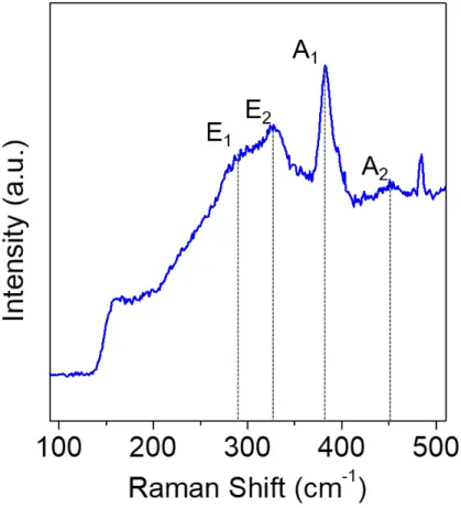
characteristic peak a labeled E2g and A1g which correspond to
LIST OF FIGURES xx
5.19 (a) Schematic of proposed thermal conductivity measurement method. The red cone symbolize focused Gaussian beam chopped at a certain frequency. Current under applied dc bias is measured through pre-amplifier which a fed to lock-in amplifier referenced by the laser chopper.(b) Cross-section schematic of the fabricated device. (c) Typical reflection map obtained by SPCM. scale bar is 5µm(d) Photocurrent map under zero applied bias. Photocurrent generated due to Seebeck at the metal-TaS2 junctions can be seen.
(e) Photocurrent map under 50mV applied bias. Negative photore-sponse can be seen coming from whole crystal. The photocurrent at suspended part of crystal is distinctly decreased. (f) Line traces through the dashed lines drawn over zero and 50mV photocurrent maps. (g) Resistance change extracted for each laser position cor-responding to photocurrent trace line plotted. Reproduced from ref. [115]. Copyright IOP Publishing Ltd. 2020. . . 83 5.20 (a) Optical microscope image of fabricated device.(b) Reflection
map obtained during SPCM.(c),(d) and (e) shows photocurrent maps under 0mV, 50mV and -50mV respectively.(f) Correspond-ing resistance change plotted as a function of laser position. Re-produced from ref. [115]. Copyright IOP Publishing Ltd. 2020. . 84 5.21 (a)Optical image of fabricated top indium contact device.(b)
Re-flection map of the same device obtained by SPCM.(c)-(d) pho-tocurrent maps collected under 400mV and -400mV applied bias respectively.(e) Characteristic current vs voltage plot in a bias sweep range of 400mV to -400mV.(f) Line traces from the pho-tocurrent maps through the center of the hole for different applied biases.(g) Corresponding resistance change plotted as every laser position. Reproduced from ref. [115]. Copyright IOP Publishing Ltd. 2020. . . 86
LIST OF FIGURES xxi
5.22 (a)Optical image of fabricated top indium contact device.(b) Re-flection map of the same device obtained by SPCM.(c)-(d) pho-tocurrent maps collected under 400mV and -400mV applied bias respectively.(e) Characteristic current vs voltage plot in a bias sweep range of 400mV to -400mV.(f) Line traces from the pho-tocurrent maps through the center of the hole for different applied biases.(g) Corresponding resistance change plotted as every laser position. Reproduced from ref. [115]. Copyright IOP Publishing Ltd. 2020. . . 87 6.1 TaS2 crystal transferred over array of holes prepared by electron
beam lithography and ICP etching. Several similar samples were prepared to study mechanical properties of this material. . . 90 6.2 Optical image of KMnO2 device. Graphite crystals exfoliated and
transferred deterministicaly on top of hexagon shaped KMnO2
crystal with extremely fine alignment. Indium needles can be seen in bright silver contrast contacted with graphite electrodes for elec-trical connection. . . 91
List of Tables
4.1 Comparison of thermal conductivities of different 2D materials measured using raman thermometery method. Reproduced from ref. [104]. Copyright John Wiley & Sons, Ltd. 2017 . . . 52 5.1 Thermal conductivity(κ) values calculated for four different
sam-ples. Different laser powers along with wavelengths used to mea-sure thermal conductivity. All yielded similar κ values with in error margin. Reproduced from ref. [115]. Copyright IOP Publishing Ltd. 2020. . . 85
Chapter 1
Introduction
We are surrounded by the world of 3D objects if we look around. Most materials that we encounter in our daily lives are three dimensional materials. If we look at their structure, we will notice that atoms in those materials are stacked up and arranged in a regular crystalline pattern. This arrangement can be analogous to the pile of oranges stacked up in a market shop. There exist another class material in which atoms are arranged in layers with each layer stacked on top of each other. It can be analogous to sheet of papers lying on top of each other. Materials with stronger in-plane bonds and weaker out of plane bonds can be categorized as layered material[1]. As a consequence of weak out of plane bonds, these layers can be separated from their bulk counterpart down to single layer of material. Based on composition there can be two major classifications of layered materials.
1. Elemental layered materials 2. Compound layered materials
1.1
Elemental Layered Materials
As suggested by the name, layered materials constitute of single element can be termed as elemental layered material. As we thin down from few layer to monolayer, the material can be called 2D material. Isolation of atomically thin single layer of carbon atoms led to the discovery of graphene by Novoselov and Geim back in 2004[2]. This was first detailed study on 2D materials. Their ground breaking experiments on graphene won them 2010 Nobel prize in physics. Graphene is single layer of carbon atoms which are very strongly bonded with each other via covalent bonds but has very weak van der Waals forces between layers which make it easier to exfoliate. It has closely packed carbon atoms arranged in a honey comb lattice. It has sp2 hybridization between carbon atoms. Fig.1.1 shows the schematic of single layer of graphene.
Figure 1.1: Schematic of graphene layer containing carbon atoms closely packed in honey comb lattice.
Other examples of elemental 2D materials include germanene[3][4], phosporene[5][6], borophene[7][8], antimonene[9][10], silicene[11][12] etc. All of these mentioned material exhibits very unique properties in the 2D limit due to strong quantum confinement and higher surface area which yields high surface activity[13][14].
1.2
Compound Layered Materials
Layered materials constitute of more than one elements in their layers are termed as compound layered materials. Some examples of compound layered materi-als include transition metal dichalcogenides(TMDCs), transition metal oxides, double hydroxides, boron nitride etc. TMDCs have gathered quite significant importance because of their extraordinary properties when exfoliated down to monolayer. One of the major advantage of TMDCs is the presence of tunable band gap which is absent in graphene[15]. TMDCs have been studied extensively in past decade and found potential applications in biosensors[16][17][18], photo detectors[19][20], memristors[21][22], field effect transistors (FET)[23] etc.
1.3
Transition Metal Dichalcogenides
Transition metal dichalcogenides is a family of 2D materials with a general for-mula MX2 where M refers to transition metal atom(Mo, W, Nb, V, Ta etc.)
and X refers to chalcogen atom(S, Se, Te). Historically, TMDCs were discovered structurally for the first time by Linus Pauling back in 1923[24]. More than 40 layered TMDCs were known by the end of 1960. Obtaining very thin layers of MoS2 using adhesive tape was realized back in 1963. Monolayer suspension of
MoS2 was obtained in 1986 for the first time. Followed by this, Reshef Tenne
suc-cessfully synthesized WS2 nanotubes along with MoS2 nanotubes later on. After
the discovery of graphene in 2004, the research in the field of layered materials including TMDCs accelerated tremendously.
1.3.1
Structure
TMDCs exist in several structural phases depending on the coordination of tran-sition metal atom. The most common phases are named as 2H, 3R and 1T . 2H crystal phase is hexagonal symmetric with trigonal prismatic coordination having
Figure 1.2: Atomic structure schematics of TMDCs showing tetragonal octa-hedral(1T), hexagonal trigonalprismatic(2H), and rhombohedral trigonal pris-matic(3R) crystal phases in monolayer form[25]. Copyright Springer Nature 2019. two layers per hexagonal unit cell. 1T phase is trigonal symmetric with octahe-dral coordination having one layer per unit cell[26]. 3R phase has rhomboheoctahe-dral symmetry with trigonal prismatic coordination with three atomic layers per unit cell. These crystal phases can be characterized in terms of different stacking order of the three planes of transition metal and chalcogen atoms which are involved in the formation of single layer of these materials . The 2H phase corresponds to ABA stacking where A refers to chalcogen atomic layer and B corresponds to transition metal atomic layer. Chalcogen atoms occupy the same position in different atomic layers named as A and lie on top of each other in the direction normal to the layer. Contrary to this, in ABC stacking, chalcogen atoms does not occupy the same position and this type of stacking is present in 1T phase. In both
stacking, transition metal atom is sandwiched between chalcogen atoms. If we look at periodic table, groups IV, V, VI, VII, IX and X contain transition metal elements. Chalcogen elements (S, Se and Te) lie in group XVI of the periodic table. Depending on the specific combination of transition metal and chalcogen atom, 2H, 3R and 1T are thermodynamically stable phases. Apart from these, some other meta-stable phases also exist like orthorohmbic 1Td phase. If we look
at group VI Mo and W elements, there are six possible combination of TMDCs formation with S, Se and Te. Out of these six, five can exist as stable 2H phase and meta-stable phase 1T[27][28][29][30]. Only WTe2 is an exception where room
temperature stable phase is orthorohmbic 1Td[31][32].
Figure 1.3: Periodic table showing classification of different elements. Each color describe certain type of element. Purple color on this table represents transition metal elements and orange color is representing S, Se and Te along with some other elements. Copyright Encyclopedia Britannica
Apart from these phases mentioned above, TMDCs can also exist in distorted phases like 1T’. In this scenario, metal-metal bond can result in dimerization of 1T phase which ultimately yields formation of 1T’ phase. Some of the examples of 1T’ phase include MoTe2 and MoS2[33][34]. Transition from one phase to other is
also possible by different methods. Laser induced transformation from 2H phase to 1T’ phase of MoTe2 has been demonstrated by Suyeon Cho et.al[35]. Phase
engineering using chemical treatment has already been demonstrated for the case of MoS2. Treating MoS2 with n-butyle lithium can assist electron donation in
the system which lead to selective phase transformation as can be seen in figure 1.4(b) [36].
(a)
(b)
Figure 1.4: (a) Laser induced phase transformation of MoTe2 from 2H phase to
1T’. Copyright American Association for the Advancement of Science 2015(b) CVD grown 2H-MoS2 crystal selectively converted to 1T phase upon treatment
with n-butyl lithium. Copyright Springer Nature 2014
1.4
Metallic Transition Metal Dichalcogenides
Metallic transition metal dichalcogenides (MTMDC) posses a finite density of state at the Fermi level which is not the case for semiconducting TMDCs. This makes the research field of MTMDCs quite distinguished when compared with STMDCs. MTMDCs can be synthesized with various chemical deposition meth-ods like CVD[37], MOCVD[38], CVT[39], MBE[40] and as simple as mechanical
exfoliation of atomically thin layers of these materials from the bulky counter part[41]. Some of the exotic phenomena that these material exhibit include charge density wave, superconductivity and magnetism. Charge density wave is an ordered quantum fluid of conduction electrons which act as a standing wave and some time may carry electric current. 2H-TaS2 is one of the exemplary
ma-terial which exhibits both charge density wave transition and superconductivity at cryogenic temperatures. The external parameters can effect the transitions very significantly. The affect of pressure on these properties has been reported by Hafeiz et.al[42]. As can be seen in 1.5 (a), the kink around 75K represent CDW transition for both in-plane and out of plane resistivity represented by ρab and ρc
respectively. The inset of figure shows superconducting transition beyond temper-ature 0.9K. Figure 1.5 (b) shows the effect of pressure on the transport properties. The CDW transition becomes insignificant at elevated pressures while the super-conducting transition temperature increases from 0.9K(atmospheric pressure) to 4.2K(3.1 GPa) and 9K(8.7GPa) as shown in the inset of same figure.
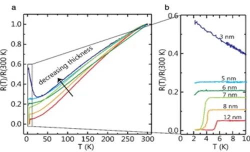
The onset of superconducting transition can heavily depend on the number of layers of the material. Thickness dependent superconductivity has also been reported in 2H-NbS2[43]. Figure 1.6 (a) shows resistance vs temperature
mea-surements performed on 2H-NbS2 crystals with different thicknesses.
Supercon-ductivity transition can be observed at a temperature as high as 6K for a crystal of thickness 12nm. Upon decreasing the number of layers, the transition tem-perature shifts to lower temtem-perature values. For crystals below 6nm thickness, no superconducting transition is observed due to possible inevitable degradation due to oxidation of the material.
Apart from interesting exotic phenomena that exist in MTMDCs, these mate-rials can be used as a promising 2D electrode instead of gold or platinum. Several report have been made to date in which using MTMDCs as electrode material en-hanced the performance of 2D material based field effect transistors. Zhang et.al. demonstrated that edge epitaxially grown NbS2 along the WS2 flake enhanced
the on and off ratio of the fabricated transistor where NbS2 acted as electrode
material[44]. The use of these materials in flexible electronics can also increase the durability of such devices[45].
Figure 1.5: (a) In-plan (ρab) and out of plane (ρc) resistivity plotted as a
func-tion of temperature at ambient pressure. The kink shows CDW transifunc-tion. Inset shows superconducting transition below 0.9K temperature. (b) Resistivity mea-surements at higher pressure. The CDW transition suppresses at very high pres-sure while the shift towards higher temperature for superconducting transition is observed(inset). Copyright Springer Nature 2016
1.5
Photocurrent Generation in
Semiconduct-ing Transition Metal Dichalcogenides
Upon illumination, almost all semiconducting transition metal dichalcogenides yield photocurrent generation. However, the mechanism that are responsible may vary from material to material. MoS2 is very well studied member of
semi-conducting TMDCs. Buscema et.al. showed that the photoresponse in monolayer across metal-semiconductor junction is dominated by photothermal effect which
Figure 1.6: (a) Normalized resistance vs temperature plotted for 2H-NbS2 for
various thickness crystals. (b) The data in the rectangular window in (a) to see superconducting transition between 0K to 10K. Copyright IOP Science, The Japan Society of Applied Physics, 2019
results due to the difference in the Seebeck coefficients of MoS2 and gold[46].
Later on, Chiang Wu et.al demonstrated that at finite applied bias the photocur-rent generation in MoS2 monolayer is due to electric field induced separation of
the carriers[47]. Similar studies are reported for several other semiconducting TMDCs as well. The detailed discussion of mechanisms will be provided in the next chapter.
1.6
Thermal
Conductivity
of
TMDCs
and
Nano-Sheets
Thermal conductivity is characterized by the ability of a material to conduct heat. Several methods in literature have been reported so far to measure thermal conductivity of TMDCs and nano-sheets. Each of the reported methods have its own advantages and disadvantages as compared to each other. 2D materials like
graphene and hexaboron nitride exhibits exceptionally high thermal conductiv-ity as compared to other similar materials[48]. Graphene has a reported value of thermal conductivity in the range of 4800-5300 Wm−1K−1 as compared to its bulk counterpart graphite which has thermal conductivity of as high as 470 Wm−1K−1[49][50][51]. Reported thermal conductivity of most studied TMDCs like MoS2 and WS2 are 34.5Wm−1K−1[52] and 32Wm−1K−1[53] respectively.
De-tailed discussion on different methodologies to calculate thermal conductivity of TMDCs and nano sheet is provided in chapter 4.
1.7
Thesis Motivation and Outline
Photocurrent generation has been studied extensively for semiconducting tran-sition metal dichalcogenides with several proposed mechanism in the literature. However, no studies have reported photocurrent generation in metallic TMDCs. As photocurrent generation in metallic TMDCs is unprecedented, the mecha-nism for such phenomenon required investigation. Few examples in literature exist where photocurrent generation through metallic materials is demonstrated. These include carbon nano-tubes and gold nano-particles. In this thesis, we ex-plore the mechanism which will be responsible for photocurrent generation in metallic TMDCs. We discussed in detail photo-thermal and photo-bolometric origin of photocurrent through metallic TMDCs starting with NbS2 as an
ex-emplary material. Once we established photo-bolometric origin of photocurrent through metallic TMDCs, we utilized this property to introduce a novel method to calculate thermal conductivity of nano-sheet using photo-bolometric effect. Our proposed method is simple in terms of calculation and device fabrication as compared to other methods that already exist in literature.
First of all, in this thesis, I will discuss several photocurrent generation mech-anisms that exist in 2D materials as can be seen in chapter 2. In chapter 3, I will discuss the photocurrent generation metallic TMDCs and governing mech-anism. Chapter 4 gives brief introduction to methods of thermal conductivity that has already been reported in literature. In chapter 5, I describe in detail our
proposed method based on bolometric effect to calculate thermal conductivity of nano-sheets along with its pros and cons. Finally, In last chapter I will give concluding remarks regarding our findings during my PhD studies.
Chapter 2
Photocurrent generation and
possible mechanisms in 2D
materials
When a photo-sensitive device like a photo diode is exposed to a certain threshold radiant power, it results in generation of photocurrent through the device. Based on nature of the material used in the device fabrication, we can have several dif-ferent mechanism that can explain the origin of current produced upon exposure to radiation. I will be discussing each of these possible mechanism one by one in the below text.
2.1
Mechanisms of photocurrent generation
Generation of photocurrrent in 2D materials can be explained by many mecha-nisms. Some mechanisms involve electric field driven separation of electron-hole induced by photon absorption. Photoconduction, photovoltaic effect and the photogating mechanisms can fall under this category. Photocurrent can also be generated by a thermal process which may include photothermoelectric and
bolometric effect. Brief discussion on each of the above mentioned mechanisms is discussed below.
2.1.1
Photo-conductive effect
When some non-metallic materials absorb photon energy, they exhibit an increase in the electrical conduction (or reduction in resistance)[54][55][56][57]. Some semi-conducting materials which are normally poor electrical conductor can observe increase in their conductivity upon illumination by a certain wavelength light[58]. The incoming photon can interact with the electrons by exciting them and ulti-mately move them to the conduction band where they can move more freely. This results in enhanced electrical conductivity[59]. This increase in the available free charge carrier makes these materials better conductors upon illumination. The rate of excitation and relaxation of these extra free charge carriers can play a determining role in estimating the change in the conductivity caused by the in-cident flux of photons[60]. The term describing the excitation and relaxation time is referred as lifetime of the the excited charge carriers. The time these excited charge carriers spend in conduction band before relaxation is termed as lifetime[61].
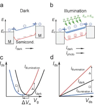
Fig.2.1 shows schematic of the band alignment of a semiconducting material upon contact with two metal electrodes under applied bias. In Fig.2.1(a), the schematic shows movement of carriers in dark condition under certain applied bias. A small drain source current (Idark) passes through the system. When
illuminated by light of energy larger than the band gap (Eph >Ebg), the electron
hole pairs are generated which are separated by the applied voltage bias. The photogenerated free electron hole carriers drift in the opposite direction towards metal electrodes. This in turn results in the enhancement of the conductivity and hence a photocurrent (Iphoto) of magnitude higher than Idark flows through
the system.
When we consider case, where mobilities of both electron and holes possess large difference from each other, it will result huge difference in electron-hole
Figure 2.1: (a) Schematic of band alignment when two metal contacts are made to semiconducting material under some applied bias without illumination. (b) Bang alignment under applied bias when a device is illuminated with photons of energy Eph greater than band gap Ebg. (c) Current plotted against applied
gate voltage with and without illumination. (d) IV plots in dark (black line) and under illumination(red solid line). Reproduced from Ref. [62] with permission from The Royal Society of Chemistry.
transit time which can be referred as τtransit and is given by equation 2.1[56].
τtransit=
L2
µ.Vds
(2.1)
Here, L is the transistor channel lengt, µ is the mobility of charge carriers and Vds is the applied drain-source bias. If the electron mobility is much higher than
the hole mobility, the photogenerated electron will pass the channel much quicker as compared to the photogenerated holes. Many electrons can contribute towards photoconductive gain (G) until electron-hole recombination. In simple words, we can say that we can extract more and more electron from a single photon which can result in a quantum efficiency greater than one. The photo-conductive gain
can be defined as the ratio of photo-generated carriers life time and transit time and can be represented by the equation 2.2. It can be clearly seen in the equation that larger value of τphotocarriers will result in larger value of G[56].
G = τphotocarriers τtransit
(2.2)
2.1.2
Photo-gating effect
Another mechanism which is based on electron-hole separation is photo-gating. It can be considered as special case of photo-conductive effect in which electron or holes can get trapped in local states where they start acting like a local gate which in result modulates the resistance of the material[63][64][65][66]. In this scenario, photo-carrier lifetime is only restricted to recombination life time of the trap states which are localized. Surface of the materials which are semiconducting in nature and defects sites acts as a host for these trap states where these trap states can last for longer period of time. This effect become very significant in materials like colloidal quantum dots, 2D semiconducting materials and nano wires in which electrical properties rely on larger surface and reduced screening[67][68][69].
Fig. 2.2(a) shows band diagram of a semiconducting material in contact with two metal electrodes under applied bias in dark condition. As can be seen, small current (Idark) passes through the system. Upon illumination, generation of
elec-tron hole pair occur. As can be seen in fig. 2.2 (b) schematic, hole are trapped at band edge where they act like a local gate. This produces a field effect which in response drives the photocurrent(Iphoto) through the system. Fig. 2.2 (c) reflects
the variation of source drain current(Ids) with respect to applied gate voltage (Vg).
There occurs a horizontal shift in the curve upon illumination termed as ∆Vg,
also marked on the plot. Solid black line shows response under dark condition while solid blue/red line shows the curve behavior under illumination. Fig. 2.2 (d)shows the IV characteristic curve under dark condition demonstrated by solid black line and under illumination at different applied gate voltage represented by solid red and blue lines. It can be seen that red IV (positive photocurrent) curve
Figure 2.2: (a) Schematic of band alignment when two metal contacts are made to semiconducting material under some applied bias without illumination. (b) Bang alignment under applied bias when a device is illuminated with photons of energy Eph greater than band gap Ebg. Holes are shown to be trapped at th band
edge. Upon illumination and under applied bias, field effect produces electrons in the channel which contribute towards photocurrent generation. (c) Current plotted against applied gate voltage with and without illumination. (d) IV plots in dark (black line) and under illumination(red and blue solid lines). Reproduced from Ref. [62] with permission from The Royal Society of Chemistry.
is obtained by the gate values used from the triangle marked range in fig. 2.2 (c) while blue IV curve (negative photocurrent) is obtained by square marked range in the panel c.
Practically, both photoconductive and photogating effect are not easily dis-tinguishable. They may co-exist in the same system. However, Furchi et al successfully demonstrated that both effect can be distinguished based on their difference in the time scales[70].
2.1.3
Photovoltaic effect
When an internal electric field separates the photogenerated electron-hole pair, then this effect is called photo voltaic effect[71][72][73]. This internal electric field can originate from the formation of PN-junction or a schottky barrier at the metal and semiconductor interface as can be seen in fig.2.3(a). IV characteristic curve exhibits non-linear behavior in both of these junction formation under dark condition. In PN junction formation, the forward bias current increases exponentially as given by relation in equation 2.3 [74].
Ids ∝ eVds− 1 (2.3)
In reverse bias configuration, negligibly small current pass through the device until the break down voltage of the junction. When the device is illuminated under zero applied bias, the photo excited electron-hole pairs gets separated by the internal electric field. This in response produces significant amount of photo-current which can be referred as short-circuit photo-current(Isc). If the circuit is kept
open, the charge carriers with opposite polarities can be restricted in different parts which in response will lead to generation of a voltage. This net voltage is termed as open circuit voltage(Voc). When we illuminate the device and apply
reverse bias, an increase in reverse current is observed as the junction electric filed sweeps the photoexcited charge carriers in the opposite direction. Compared to photoconducting effect, in photovoltaic effect, generated photocurrent can be converted to electrical power[75].
Current vs voltage graph of the PN junction both in dark (solid black line) and under illumination (solid red line) is shown in the fig. 2.3(b). The curve under illumination appear shifted downwards when compared to dark current curve as the generated photocurrent has similar sign as the reverse bias current. It is worth noting that the portion of the curve lying in the lower left quadrant of the plot where the current has negative values under positive applied bias, can be used to calculate maximum electrical power as indicated by Pmaxel on the plot.
Figure 2.3: (a) Schematic of a PN-junction formation. Common fermi energy (Ef) level for both P and N doped semiconductor can be seen in the schematic
represented by dashed black line. The incident photon of energy larger than band gap of the material (Eph¿ Ebg) generates the electron hole pair as represented by
black and white dot respectively. The built in electric field at the PN-junction then separates the electron hole pair and gets accelerated. (b) Ids vs Vds curves
plotted in dark and under illumination represented by black and red lines respec-tively. A short circuit current due to open circuit voltage is generated in the device upon illumination. An electrical power is generated by the device indi-cated by Pmax
el (maximum power). Reproduced from Ref. [62] with permission
from The Royal Society of Chemistry.
2.1.4
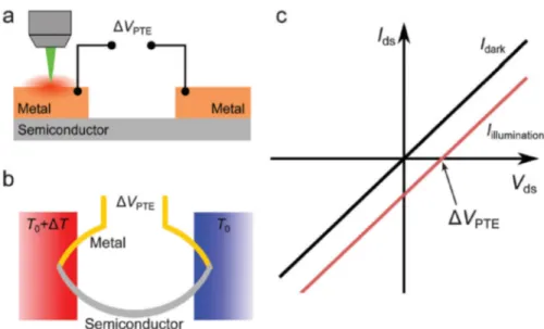
Photo-thermoelectric effect
When a heat gradient is generated through a material by light induced heating, there will appear a temperature gradient between the two ends of the material. This temperature gradient can be termed as ∆T. This ∆T can be converted to a potential difference because of the Seebeck effect or photothermal effect[76]. This potential difference is linearly proportional to the temperature gradient and can be expressed by the equation
∆V = −S.∆T (2.4)
Where S is the seebeck coefficient.
The temperature gradient can be created with focused laser spot locally whose dimensions are much smaller than the whole device[77]. Global illumination can
Figure 2.4: (a) Schematic of a FET which is being illuminated locally using a fo-cused laser spot at one of the metal-semiconducting junction. The configuration represent the open circuit case where the thermoelectric potential is generated between the two junctions. (b) represents the circuit diagram of the same device depicted in (a). (c) IV characteristic curve in both dark (black) and under illu-mination(red) are plotted. Under zero bias, a current is generated in the system driven by the thermoelectric potential difference(VP T E). Reproduced from Ref.
[62] with permission from The Royal Society of Chemistry.
also generate such regions of temperature gradients in a material which exhibits different absorption of photon energy in different part of the device[78].
Due to photo-thermoelectric effect, a temperature gradient generates a poten-tial difference through the device which in response can drive current through the system even under zero applied bias. A schematic of such device is shown in fig. 2.4(a) where two junctions are maintained at different temperatures by the aid of focused laser spot. A potential difference (VP T E) is generated due to this
constant temperature gradient between the two junctions which can be expressed by the equation 2.5[79].
In this equation, we can neglect the term Smetal.∆T because of smaller values
of seebeck coefficients of metals as compared to semiconducting materials. The estimation of ∆T can be done using finite element analysis methods or incorpo-rating on chip thermometers on the device[80][81]. After knowing the value of ∆T, the corresponding Seebeck coefficient can be estimated. Potential difference values generated by photothermal effect can range from tens of micro-volts to tens of mili-volts. It is important to have ohmic contact formation in order to observe photo-thermoelectric effect. In a scenario, where illumination is on top of uniform semicoducting channel, no current will flow through the device as there is no bias applied to system. Also, the temperature gradient will be negligibly small in this case and the required potential difference will not be created to drive the current.
IV curves of a device in which PTE is dominant is shown in fig. 2.4(c). As the curve under dark condition exhibit linear behavior giving strong indication of formation of ohmic contacts with negligibly small schottky barrier. When the device is illuminated, current at zero applied bias is observed with out changing the resistance of the device due to the photothermoelectric effect. Intersection of red curve with the zero current axis give the value of ∆VP T E as indicated by
black arrow in fig. 2.4(c).
2.1.5
Photo-bolometric effect
When the uniform heating induced by photon absorption ultimately change the resistance of the material, such effect is termed as photo-bolometric effect[82][83]. This effect has direct relationship with the change of conductance of a material with temperature (dG/dT) and uniform increment in the temperature by the laser induced heating of the material. Many IR detectors works based on this principle in a four terminal configuration which enhance the detectivity of the operational device[84].
Chapter 3
Photo-current generation in
metallic transition metal
dichalcogenides
Several mechanisms play their role in generation of photocurrent in 2D semicon-ducting layered materials[85][86]. These mechanism may involve photothermal effect, photovoltaic effect, photoconduction and photogating. I have discussed briefly all these mechanism in the previous chapter. Apart from few exceptions, the above mentioned mechanisms do not result photocurrent generation in metal-lic materials. As the thermal conductivity of metalmetal-lic materials is generally higher and have low absorption of optical excitation, the photothermal effect becomes very insignificant in these materials. Also, Under certain applied bias, electron that are being excited optically in metals will have negligible contribution to-wards the already existing huge number of intrinsic electron close to the Fermi level. Some of the metallic systems in which photocurrent generation has been reported include gold nano particle network[87], graphene[85][88] and metallic carbon nanotubes[89]. As photocurrent generation in metallic transition metal dichalcogenides(TMDCs) is not expected, the possible mechanism for such phe-nomenon has not been explored so far. In this chapter, I will be discussing pho-tocurrent generation through mechanically exfoliated Niobium Disulfide(NbS2)
using scanning photocurrent microscopy. According to our findings, the pho-tocurrent generation in such system is mainly due to photothermal effect and will be discussed in detail later in this chapter.
3.1
Experimental methods
3.1.1
Bottom contact devices
Bottom contact devices are fabricated by transferring selected crystal on top of pre-patterned gold electrodes. In these devices, the gold electrode are lying under crystal making contact to the bottom side of the crystal. This is why these devices are referred as bottom contact devices. The fabrication process is described in detail in the following sections.
3.1.1.1 Mechanical exfoliation
3R-NbS2 bulk source is purchased from HQ graphene. The bulk source is pasted
against a yellow kapton tape and peeled off very carefully using clean tweezers to avoid any contamination. This will leave layers of the pasted material onto the tape. The tape containing NbS2 crystals is pasted against a cleaned 280nm
SiO2/Si chip and placed on hot plate heated to 900C for 1 minute. Then the
tape is peeled off from the SiO2/Si substrate leaving behind exfoliated crystals of
NbS2 onto the substrate. The sample is observed under microscope in order to
target a suitable crystal for device fabrication.
3.1.1.2 Optical lithography and metal evaporation
Gold electrodes are pre-patterned onto a clean 280nm SiO2/Si substrate using
optical lithography. First of all the sample is rinsed with acetone, iso-propanol followed by thorough rinsing with DI water. The substrate is placed onto hot
plate set at 1200C for 10 minutes to get rid of all possible moisture. Positive
toned photo-resist AZ-5214 is spin coated onto the cleaned substrate at 4000rpm. The sample is then placed onto hot plate for soft bake to activate the photo-resist. The chip containing photo-resist is exposed to UV light mounted onto a mask aligner under a mask containing desired features. The dose of exposure is set to 40mJ/cm2. After exposure, the chip is dipped in developer AZ-400K. The developer is a solution of 20mL AZ-400k in 80mL water which make it 1:4 solution. The optimized development time is 45 seconds. After that the required feature are patterned onto the desired substrate. Followed by this, we evaporate gold as metal contact material. 5nm chrome is first deposited as an adhesion layer for gold using thermal evaporator. 100nm gold is then deposited which act as electrodes after the successful lift-off. Fig.3.1 shows final result of electrodes patterned following the above mentioned procedure.
Figure 3.1: Array of two terminal electrodes patterned using optical lithography
3.1.1.3 Deterministic crystal transfer
Selected crystals after mechanical exfoliation are transferred on top of pre-patterned electrodes deterministically using a polymer film. We use poly-carbonate(PC) as a polymer for this purpose. A small piece of thin PC film
Figure 3.2: Schematic of the deterministic crystal transfer starting from mechan-ical exfoliation of the NbS2 till the selected flake aligned and transferred on top
of metal electrode.
is cut and placed on top of our desired crystal. The film is allowed to melt by increasing the stage temperature to 1650C. Once the film is melted, the sample
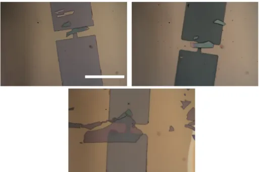
is removed from the stage and the PC film solidifies again. The film is carefully peeled from the substrate which will pick up our desired crystal from the sub-strate. This film then placed on the pre-patterned substrate containing several gold electrode. The film is then manipulated using a fine needle mounted on a micro-manipulator to align our desired crystal accurately with the electrodes. Once the crystal is aligned, the stage temperature is increased again to melt the PC film again. This step will make sure that our film does not move once we put it into organic solvent for dissolution of the PC film. The sample is then immersed in chloroform to dissolve PC film for 15 minutes. The samples is removed very gently from chloroform solution after 15 minutes and observed under microscope. Schematic of the whole process can be seen in figure 3.2. Optical microscope and scanning electron microscope images of the fabricated devices can be seen in figures 3.3 and 3.4 respectively.
Figure 3.3: Optical microscope images of back contact devices. scale bar is 30µm
Figure 3.4: Electron microscope images of back contact devices showing top view and side view of the devices.
3.1.2
Top contact devices
In top contact devices, the gold electrodes are deposited on top of selected crystal. In order to obtain such devices, I utilized two different lithography techniques.
1. Optical lithography
2. Electron beam lithography
3.1.2.1 Optical lithography
After doing mechanical exfoliation of the selected material, a suitable crystal is chosen to put metal contact on top of it. The orientation along with the location of the crystal is roughly noted under microscope. If needed a scratch mark is placed near the crystal using a diamond scriber. It helps in locating the crystal under mask aligner in a more efficient and less time consuming way. The pat-terning parameters are same as described in section 3.1.1.2. After spotting the crystal under the mask aligner, the crystal is aligned with the electrode terminals followed by UV exposure. After development, the patterned crystal is observed under microscope. If patterning is successful, the sample is placed safely in a container and more similar samples are prepared for metal evaporation. After metal evaporation and successful lift-off process, we observe fabricated devices under microscope.
Figure 3.5: Optical micrographs of the fabricated devices top contact devices using optical lithography. Scale bar is 30µm
Figure 3.6: Electron microscope images of top contact devices showing top view and side view of the selected device.
3.1.2.2 Electron beam lithography
Some of the devices in this study are fabricated using electron beam lithography. It is a direct writing technique which does not require any physical mask for patterning and we can control the dimensions of each pattern separately that we want to print. This technique can easily have a nano-meter precision in patterning. It is a two step electron beam lithography process. In order to be able to pattern, mechanical exfoliation of desired material is performed on a rectangular chip with flat sides and sharp corner. We can choose one sharp corner of the chip as origin and get the coordinates of the crystal lying on the chip using an on-screen digital ruler named MB-ruler. The precision of the coordinates can be of the order of few tens of micrometer.
In next step, spin coating of electron resist is performed. We use polymethyl methacrylate(PMMA) resist for this purpose. A double layer of two different type of PMMA resist is spin coated. First layer is spin coated PMMA 495(A6) at 4000rpm for 60 seconds followed by a prebaking step for two minutes at a temperature of 1800C. After this another layer of PMMA 950(A6) is spin coated following similar parameters followed by same duration of baking at 1800C.
First of all, four alignment cross marks along with three squares are patterned in the vicinity of the target crystal. As sample is coated with electron beam resist, we can not image the crystal in the electron microscope. We use these alignments crosses and squares to match with the actual design prepared as a GDS file in K-Layout software. Once these alignment marks are match perfectly with the actual GDS design, we can draw the desired features and electrodes on the same file. We used EFI Nova 600 NanoSEM for our electron beam lithography process. The used voltage for our process is 30KV to ensure maximum penetration depth. The beam current is chosen according to the feature size. For smaller feature of the order of 2 to 3 µm I used 52pA. For larger features of the order of 100 to 300 µm, I used 80nA. The dose was chosen to be 100µC/cm2.
![Figure 1.2: Atomic structure schematics of TMDCs showing tetragonal octa- octa-hedral(1T), hexagonal trigonalprismatic(2H), and rhombohedral trigonal pris-matic(3R) crystal phases in monolayer form[25]](https://thumb-eu.123doks.com/thumbv2/9libnet/5932041.123368/26.918.247.714.159.669/structure-schematics-tetragonal-hexagonal-trigonalprismatic-rhombohedral-trigonal-monolayer.webp)