W1E.2.pdf CLEO Pacific Rim 2018 © OSA 2018
Laser writing of nanostructures deep inside
Gallium Arsenide (GaAs)
Onur Tokel1,2, Ahmet Turnali3, Petro Deminskyi1, Serim Ilday,2, and F. ¨Omer Ilday1,2
1Department of Physics, Bilkent University, Ankara, 06800, Turkey
2UNAM - National Nanotechnology Research Center, Bilkent University, Ankara, 06800, Turkey 3Department of Electrical and Electronics Engineering, Bilkent University, Ankara, 06800, Turkey
Abstract: Recently, we have showed a direct laser writing method that enables the first subsurface modifications and functional devices created deep inside silicon. Here, we extend the technique demonstrating the first controlled subsurface nanostructures in GaAs.
OCIS codes: 220.4241, 350.3390, 130.3130, 140.3440
Laser structuring of semiconductors has been studied since the 1970’s [1]. Most notably, for silicon wafers, available methods had not been successful in breaking the dimensional barrier to enable fabrication of buried structures deep inside the wafers without damaging the wafer above of below the modifications. We had solved this problem by introducing a novel approach based on nonlinear laser interactions, resulting in a single-step, maskless laser writing deep inside silicon, which can be used to create highly-controllable modifications in the bulk of silicon without damaging the surface (Tokel et. al. Nature Photonics, 2017) [2]. Using this novel method, we demonstrated the first optical elements buried deep inside silicon [2]. While silicon is the most important semiconductor within which laser-induced modifications were lacking, it is clear that a similar problem continues to plague various important semiconductors, notably Gallium Arsenide (GaAs). In this work, we extend the 3D nonlinear laser lithography approach we developed for Si [2] to GaAs, and report to the best of our knowledge the first nanostructures observed deep inside GaAs wafers.
The interest in GaAs is due to the fact that it is a direct bandgap semiconductor with high quality epitaxial growth [3]. Thus, it is used in various optoelectronic and integrated devices, including highest-efficiency solar cells, high-efficiency light-emitting devices, and integrated circuits. However, so far conventional lithography techniques can only be used to create structures and fabricate functional elements on the top layers of GaAs, and cannot be used to create modifications inside GaAs. This is due to the limitation that the capabilities and achievements of bulk laser processing of glasses and other materials could not be transferred into GaAs. Our novel approach [2] exploits the nonlinear effects in a semiconductor [4] along with feedback-based interactions of an infrared pulsed laser within the wafer. Here, we extend this method to realize the first subsurface laser-structuring of GaAs. Moreover, we report the first observation of nanostructures created deep inside GaAs without damaging the wafer surface.
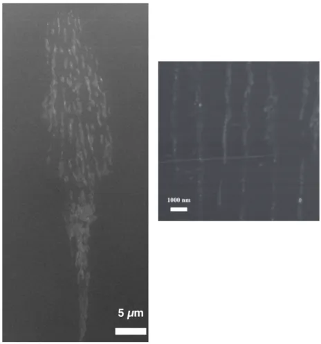
In order to achieve these, we used laser light from a home-built, all-fibre master oscillator power amplifier (MOPA) system that produces 5-ns pulses operating at 1.55 µm. This wavelength is chosen such that GaAs is mostly transparent, which enables the laser to reach deep inside the wafer without damaging its surface. The laser system is integrated to a material processing station with polarization and power control steps. A three-axis motorised stage is used to precisely position the sample with respect to the laser focus. The laser writing modality and the details of the system are similar to our previous work [2,5]. The 3D nonlinear laser lithography approach is used to create nano-structures inside GaAs (Figs. 1). We observe structures with down to 300 nm feature sizes. An interesting observation is that, we create orderly formation of subsruface structures. These quasi-periodic patterns are characterized with Scanning Electron Microscopy to have a periodicity of about 500 nm. This value is similar to the laser wavelength inside GaAs. Thus, these formations are qualitatively similar to self-organized nanogratings that have previously been observed in glasses [6,7]. After this laser processing step, these modifications can potentially be used as near-IR optical elements, similar to the subsurface modifications as realized in Si. An optional second step is used to etch out the crystal to show the modified areas in detail, which confirmed the periodicity.
W1E.2.pdf CLEO Pacific Rim 2018 © OSA 2018
Fig. 1 The SEM image of the nanogratings observed inside GaAs. After laser processing the sample is diced in order to observe its bulk. The structures carry a strong resemblance to the self-organized patterns laser-induced in glass. The laser is propagating along the vertical axis.
In conclusion, we extended the 3D nonlinear laser lithography approach to GaAs and demonstrated the first laser-nanostructuring of GaAs deep inside the wafer. The demonstrated method is maskless, rapid, inexpensive and scalable. The volume gratings were quasi-periodic, which are notable for showing a similarity to self-organization in 3D. More-over, they represent the breaking of the dimensional barrier for the technologically important semiconductor GaAs, which are likely to lead to novel optical devices directly fabricated inside GaAs.
References
1. I.W. Boyd, ”Laser processing of silicon,” Nature 303, 481 (1983)
2. O. Tokel, A. Turnali, G. makey, P. Elahi, T. Colakoglu, E. Ergecen, O. Yavuz, R. Hubner, M. Borra, I. Pavlov, A. Bek, R. Turan, D. Kesim, S. Tozburun, S. Ilday, F. ¨Omer Ilday, ”In-chip microstructures and photonic devices fabricated by nonlinear laser lithography deep inside silicon”, Nat. Photon. 11, 8639 (2017).
3. John Rogers et. al.,”GaAs photovoltaics and optoelectronics using releasable multilayer epitaxial assemblies”, Nature, 465,329 (2010).
4. J. Leuthold, C. Koos and W. Freude, ”Nonlinear silicon photonics,” Nature Photon.4, 535 (2010).
5. I. Pavlov, O. Tokel, S. Pavlova, V. Kadan, G. Makey, O. Yavuz, F. ¨Omer Ilday , ”Femtosecond laser written waveguides deep inside silicon,” Optics Letters, 42,15,3028 (2017).
6. Shimotsuma et. al., Phys. Rev. Lett. 91, 247405 (2003). 7. Yang et. al., Opt. Exp. 14,10117 (2006).