NOVEL DESIGN-BASED COMPLEX
NANOSTRUCTURES IN HYBRID
CORE-SHELL ARCHITECTURES FOR
HIGH-EFFICIENCY LIGHT GENERATION
A THESIS
SUBMITTED TO THE DEPARTMENT OF PHYSICS AND THE INSTITUTE OF ENGINEERING AND SCIENCES
OF BILKENT UNIVERSITY
IN PARTIAL FULLFILMENT OF THE REQUIREMENTS FOR THE DEGREE OF
MASTER OF SCIENCE
By
Ilkem Özge Özel
July 2010
ii
I certify that I have read this thesis and that in my opinion it is fully adequate, in scope and in quality, as a thesis for the degree of Master of Science.
Assoc. Prof. Dr. Hilmi Volkan Demir (Supervisor)
I certify that I have read this thesis and that in my opinion it is fully adequate, in scope and in quality, as a thesis for the degree of Master of Science.
Assist. Prof. Dr. Dönüş Tuncel
I certify that I have read this thesis and that in my opinion it is fully adequate, in scope and in quality, as a thesis for the degree of Master of Science.
Assoc. Prof. Dr. Ceyhun Bulutay
Approved for the Institute of Engineering and Sciences:
Prof. Dr. Levent Onural
iii
ABSTRACT
NOVEL DESIGN-BASED COMPLEX
NANOSTRUCTURES IN HYBRID CORE-SHELL
ARCHITECTURES FOR HIGH-EFFICIENCY LIGHT
GENERATION
İlkem Özge Özel M.S. in Physics
Supervisor: Assoc. Prof. Dr. Hilmi Volkan Demir
July 2010
Recent developments in nanoscience and nanotechnology have given rise to the discovery of hybrid nanostructured multi-component materials that serve several tasks all at once. A very important and rapidly growing field of these materials is the development of highly efficient fluorophores to meet the urgent demand of low-energy consuming, high-quality light emitters for future solid-state lighting applications. Such hybrid nanomaterials are entailed to exhibit extraordinary optoelectronic properties compared to the bulk case of their single components such as enhanced quantum efficiency, tunable multi-color emission, and reduction of multiple processing steps. Herein, to address these requirements, we propose and demonstrate novel design-based complex nanomaterials in hybrid multi-shell architectures for high-efficiency light generation. These requirements are made possible by using the concept of hybrid core-shell-… nanostructures comprising at least two units, including hybrid metal-core/dielectric-shell nanoparticles furnished with an outer shell of semiconductor nanocrystals for enhanced emission and different conjugated polymers forming a single multi-polymer nanoparticle and emitting
iv
simultaneously at different wavelengths. In the first part of this thesis, we developed and demonstrated Au-silica core/shell nanoparticles that successfully assemble CdTe nanocrystals right on their silica shells for enhanced plasmon-exciton interactions, while solving the common problems of lacking control in dielectric spacing and limited film thickness typically encountered in such plasmon-coupled nanocrystals. Here we present the synthesis and characterization results of this new set of multi-shell decorated nanoparticle composites with a tunable dielectric spacing thickness of silica shell precisely controlled by synthesis to optimize plasmon-exciton interactions for enhanced emission. Experimental data obtained from steady-state and time-resolved photoluminescence measurements together with extensive computational analysis clearly verify the strong plasmon-exciton interactions in these design-based multi-shell nanocomposites. In the second part, we construct bi-polymer nanoparticle systems in various architectures of core/shells, for each of which thorough investigations of the non-radiative energy transfer mechanisms are made. Here we present the synthesis and characterization results of these core/shell polymer nanoassemblies. The flexibility of designing such bi-polymer nanostructures allows for the optimization of maximum energy transfer efficiency. This concept of complex hybrid nanostructures for high-efficiency light generation opens up new paths for optoelectronic devices and nanophotonics applications including those in solid-state lighting.
Keywords: Nanostructures, nanomaterials; plasmonics, localized plasmons, metal-enhanced luminescence; exciton migration, non-radiative energy transfer, Förster resonance energy transfer (FRET); hybrid nanoparticles, metal nanoparticles; semiconductor nanocrystals, colloidal quantum dots; conjugated polymers; excitons, spontaneous emission, photoluminescence, time-resolved fluorescence; FDTD.
v
ÖZET
YÜKSEK VERİMLİ IŞIK ÜRETİMİ İÇİN MELEZ
ÇEKİRDEK-KABUK MİMARİLİ YENİLİKÇİ DİZAYN
TEMELLİ KOMPLEKS NANOYAPILAR
İlkem Özge Özel Fizik Bölümü Yüksek Lisans
Tez Yöneticisi: Doç. Dr. Hilmi Volkan Demir Temmuz 2010
Nanobilim ve nanoteknolojideki yeni gelişmeler çoklu içerikli malzeme içeren birçok görevi tek başına yapabilen melez nanoyapıların keşfine yol açmıştır. Geleceğin katı hal aydınlanma uygulamalarının acil ihtiyacı olan düşük enerji tüketimli, yüksek kaliteli ışık yayıcı ihtiyacının karşılanması amaçlı olarak yüksek verimli ışıyanların geliştirilmesi bu malzemelerin çok önemli ve hızlı bir şekilde gelişen bir alanıdır. Böyle melez nanomalzemelerin tek içerikli büyük boyutlarına göre arttırılmış kuvantum verimliliği, ayarlanabilir çok renkli ışıma ve çoklu işlem basamaklarının azalması gibi olağandışı optoelektronik özellikler göstermesini gerektirmektedir. Burada bu gereksinimleri hedefleyen yüksek verimli ışık üretimini için yenilikçi dizayn temelli çoklu kabuklu melez mimaride kompleks nanomalzemeleri teklif ediyor ve gösteriyoruz. Bu gereksinimler arttılrılmış ışık üretimi amaçlı melez çekirdek-kabuk-(…) konseptindeki en az iki birim içeren en dış kabuğu yarıiletken nanokristallerle döşenmiş metal-çekirdek/yalıtkan-kabuk nanoparçacıklar ve farklı konjuge polimerle çoklu polimer içeren ve eş zamanlı farklı dalgaboylarında ışıyan tek nanoparçacıklar ile giderilmiştir. Bu tezin ilk kısmında, arttırılmış plazmon-ekziton etkileşimleri için aynı zamanda plazmon etkileşimli nanokristallerin
vi
genel sorunu olan yalıtkan ayraç kalınlık kontrolü ve sınırlı film kalınlığı gibi sorunları çözen silica kabuğun hemen üzerinde yerleştirilmiş CdTe nanokristalleri olan Au-Silika çekirdek/kabuk nanoparçacıkların geliştirilmesi ve gösterimi vardır. Burada arttırılmış ışık yayılımı için bu yeni set plazmon-ekziton etkileşimleri optimizasyonu için kalınlığı sentez esnasında ayarlanabilir yalıtkan ayraçlı çoklu-kabuk döşenmiş nanoparçacık kompozitlerin sentez ve karakterizasyon sonuçları sunulmaktadır. Sabit ve zaman çözünürlü fotoışıma ölçümlerinden elde edilen deneysel veriler ve bilgisayarlı derin analizler bu dizayn tabanlı çoklu-kabuk nanokompozitleride güçlü plazmon-ekziton etkileşimleri olduğunu net bir şekilde göstemektedir. İkinci kısımda çift-polimer nanoparçacık sistemlerini her birinde ışık yayılımsız enerji tranfer mekanizmalarını incelemek üzere değişik çekirdek-kabuk mimarilerinde yapılandırdık. Burada bu çekirdek/kabuk çift polimer nanobirleşimlerin sentez ve karakterizasyon sonuçlarını sunuyoruz. Bu tarz çift-polimer nanoyapı dizayn esnekliği maksimum enerji transfer verimliliğinin optimizasyonuna izin vermektedir. Yüksek verimli ışık üretimi amaçlı bu kompleks melez nanoyapılar konsepti optoelektronik aygıt ve katı hal aydınlanmayı da içeren nanofotonik uygulamalarında yeni bir yol açmaktadır.
Keywords: Nanoyapılar, nanomalzemeler; plazmonik, localize plazmonlar, metalle arttırılan ışıma; ekziton göçü, ışık yayılımsız enerji transferi, Förster rezonans enerji transferi (FRET); melez nanoparçacıklar, metal nanoparçacıklar; yarıiletken nanokristaller, kolloid kuvantum noktacıklar; konjuge polimerler; ekzitonlar, kendiliğinden ışınsalım, fotoışıma, zaman çözünürlü ışıma; FDTD.
vii
Acknowledgements
I am grateful to Assoc. Prof. Dr. Hilmi Volkan Demir, for giving me the opportunity to undertake the research outlined in this thesis. Along with his positive attitude to life and his endless support, as well as his hard work on the project, his enthusiasm has maintained my growing interests in various fields of research.
It is also an honor for me to thank my co-advisor, Asst. Prof. Dr. Dönüş Tuncel, who has made her support available in a number of ways. I would like to thank her for her guidance and support in our collaborative research works. Her advice and suggestions helped me enormously over the past five years.
I would like to thank Assoc. Prof. Dr. Ceyhun Bulutay for his useful comments and suggestions as being a member of my thesis committee.
During the course of this work at Bilkent University (2008 – 2010), I was fully supported in by the TÜBİTAK National Scholarship Programme-2210 for MSc Students for which I owe special thanks.
I wish to thank UNAM and staff for providing the lab facilities and especially Mustafa Güler for taking all my TEM images and being very kind to me.
I would like to thank all former and recent group members of Devices and Sensors Group, who work under the supervision of Assoc. Prof. Dr. Hilmi Volkan Demir. I would especially like to thank Asli Yilmaz, Olga Samarskaya, Nihan Kosku Perkgoz, Hatice Ertugrul, Neslihan Cicek, Gülis Zengin, Emre Sari, Can Uran, Gurkan Polat, Murat Soganci, Akin Sefunc, Ozgun Akyuz, Emre Unal, Sina Toru, Talha Erdem, Burak Guzelturk, Ugur Karatay, and Cuneyt Eroglu for their friendship and collaborations.
viii
I would like to thank all former and recent group members of PLED Group, who work under the supervision of Assist. Prof. Dr. Donus Tuncel. I would especially like to thank Muge Artar, Vusala Imbrahimova, Eun Ju Park, Zeynep Goksel Ozsarp, Gizem Celtek, Gizem Er, Unsal Koldemir, Ibrahim Hocaoglu, for their friendship and collaborations.
There are some very special friends to me with whom some of them we have shared almost all the years at Bilkent. These are Seçkin and Özlem Şenlik, Samed Yumrukçu and Şeyda İpek. I am glad to be sharing such a nice friendship, which I hope will never end. I always feel very lucky to be their close friends. I want to say how glad I am to meet Evren Mutlugün and his wife Sümeyye who are a cheer supply for me all the time, Rohat and Bahar Melik who always treated me and Tuncay as his younger siblings, Sedat Nizamoğlu who is always kind and helpful in my research. Those are very special friends to me and they were always there when I needed them.
Last, but not least, I thank my entire extended family: my parents, Ayhan and Ilhan Huyal for giving me life in the first place, and for their unconditional love, support and encouragement to pursue my interests. I would especially like to thank my sister Simge for listening to my complaints and frustrations, and for believing in me all the time and my brother Ulaş, for always being there when I had questions and his interesting discussions on almost any irrelevant field. I would like to deeply thank to my new family members, my mother-in-law Yıldız Özel and my father-in-law Ali Özel for their sincere love as if I am their daughter, being always kind to me and supporting me in all respects and raising Tuncay up as a great person. Also my thanks go to my brother-in-law Taner and his wife Zülal Tezcan Özel for their guidance and support.
And finally, my deepest gratitude goes to my husband Tuncay Özel, without whom this thesis would not be possible. Tuncay had confidence in me when I
ix
doubted myself, and brought out the good ideas in me. His endless love and support has created what I am today for which I will be ever indebted. To him I dedicate this thesis.
x
Table of Contents
ABSTRACT... III ÖZET ... V ACKNOWLEDGEMENTS ... VII TABLE OF CONTENTS ... X CHAPTER 1...1 INTRODUCTION ...1 CHAPTER 2...7FLUORESCENT CONJUGATED POLYMERS ...7
2.1POLYFLUORENES:ANOVEL CLASS OF LIGHT EMITTING POLYMERS...7
CHAPTER 3...16
SEMICONDUCTOR NANOCRYSTALS ...16
3.1SIZE AND COLOR TUNING:THE QUANTUM SIZE EFFECT...19
3.2CDTE NANOCRYSTAL SYNTHESIS...20
3.3MEASUREMENT OF FLUORESCENCE QUANTUM EFFICIENCY...23
CHAPTER 4...25
FUNDAMENTALS OF SURFACE PLASMONS ...25
4.1OPTICAL PROPERTIES OF METALS...27
4.1.1MIE SCATTERING...34
4.1.2SIZE,SHAPE,COMPOSITION AND ENVIRONMENT DEPENDENCY OF SURFACE PLASMONS35 4.1.4METHODS FOR METAL NANOPARTICLE FORMATION...37
CHAPTER 5...39
AU-SILICA CORE/SHELL HYBRID NANOPARTICLES FURNISHED WITH CDTE NANOCRYSTALS FOR ENHANCED PLASMON-EXCITON INTERACTIONS...39
5.1STATE-OF-THE-ART...40
5.2COMPUTATIONAL ANALYSIS AND EXPERIMENTAL DEMONSTRATION WITH OPTICAL CHARACTERIZATION RESULTS OF OUR HYBRID CDTE FURNISHED AU-SILICA CORE/SHELL NANOPARTICLES...44
5.2.1SYNTHESIS,CHARACTERIZATION, AND SIMULATION OF HYBRID NANO-ASSEMBLIES....45
5.2.2EXPERIMENTAL DEMONSTRATION AND OPTICAL CHARACTERIZATION RESULTS AND NUMERICAL ANALYSIS...49
CHAPTER 6...67
NON-RADIATIVE ENERGY TRANSFER IN BI-POLYMER NANOPARTICLES OF FLUORESCENT CONJUGATED POLYMERS ...67
6.1FÖRSTER RESONANCE ENERGY TRANSFER IN ORGANIC SYSTEMS...67
6.2ANEW APPROACH FOR THE PREPARATION OF DUAL-EMITTING POLYMER NANOPARTICLES ...69
xi
6.4EXPERIMENTAL DEMONSTRATION AND OPTICAL CHARACTERIZATION RESULTS...74
CHAPTER 7...90
CONCLUSION ...90
xii
List of Figures
Figure 2.1. Chemical structure of a polyfluorene backbone with functional groups R attached at the 9th position. ... 8 Figure 2.2. Energy-minimized 3D structure of cyclodextrin-threaded
polyrotaxane with poly(para-phenylene) (β-CD-PPP) and its chemical
structure[]. ... 9 Figure 2.3. Cartoon representation of the process flow for the reprecipitation method of polyfluorene with the chemical structure of the polymer given at the bottom... 10 Figure 2.4. a) Preparation of the solid polymer nanoparticle dispersion in water. b) Polymer blend preparation from a dispersion containing nanoparticles of two different polymers, or by using dispersions that contain both polymers in each individual nanoparticle [43]. ... 12 Figure 2.5. TEM images of different biphasic blend particles with percentages of the amounts employed in the preparation given. The particles are deposited on a carbon-coated copper grid and left to dry under air. The samples are not further labeled or stained [50]. ... 12 Figure 2.6. (a) Structural formula of P3DDUT, (b-g) SEM images of
nanoparticles prepared by reprecipitation method and dynamic light scattering (DLS) size distributions, (b,e) ) 0.1 % P3DDUT/THF at 20ºC, (c,f) 1.0 wt.-% P3DDUT/THF at 20ºC, (d,g) 1.0 wt.-wt.-% P3DDUT/THF at 80ºC [44]. ... 14 Figure 2.7. (a) Absorption and (b) fluorescence spectra of P3DDUT
nanoparticles, with various mean diameters, dispersed in water [44]... 14 Figure 2.8. (a) Normalized absorption and (b) normalized fluorescence spectra of conjugated polymer nanoparticles (solid line) compared to polymers in THF solutions (dashed line). (c) Photo of various polymer nanoparticle dispersions under UV radiation [49]. ... 15 Figure 3.1. Wurtzite crystal structure of a CdSe quantum dot, where purple spheres indicate cadmium atoms and green ones selenium atoms. ... 17 Figure 3.2. (a) Cross-sectional view of a silica shell capped CdSe/ZnS
nanocrystal, and (b) chemical compounds used for the silanization of NCs. The outer surface of the silica shell is further functionalized with phosphonate and thiol groups [53]. ... 18
xiii
Figure 3.2.1. A picture of CdTe nanocrystal synthesis setup. Precursors are produced in the main flask (left) and Al2Te3 source is activated in the small
three-necked flask (right). ... 22 Figure 3.2.2. (onset) Normalized photoluminescence spectra of our CdTe NCs emitting at different wavelengths which correspond to different boiling
durations. (inset) A photo of our CdTe nanocrystals emitting in different colors depending on the size distribution... 23 Figure 4.1. (Left) The Lycurgus cup when light is shine from the outside
(reflection), and (right) when light is shine from the inside of the cup
(absorption). ... 25 Figure 4.2. Schematic representation of surface propagating and localized
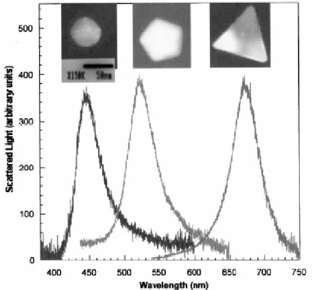
plasmons on nanostructured gold surfaces [76]. ... 27 Figure 4.1.1. Schematic representation of electric field which is created by an incident wave and corresponding shift of electron cloud resulting in a plasmon resonance of the particle []. ... 31 Figure 4.1.2. Electric field distribution of 15 nm Au metal nanoparticles at an incident planewave radiating at 520 nm, which (a) propagates along the x-axis and is polarized along the y-axis, and (b) propagates along the y-axis and is polarized along the x-axis ... 33 Figure 4.1.3. Scattered light intensities for silver nanoparticles with their
corresponding high-resolution TEM images. Particles having spherical shape peak at the blue region, pentagon-shaped particles appear green, and triangular-shaped particles appear red [91]. ... 36 Figure 5.1.1 (left) Schematic representation of the experimental setup using a scanning probe method. (right) Fluorescence enhancement factor (red curve), lifetime (brown curve) of terrylene for varying sample-particle separations [95].
... 41 Figure 5.1.2. (a) Cartoon picture of the hybrid nanostructure composed of Au nanorods, silica shell and dye molecules, (b) Chemical structure of the dye oxazine 725, (c) SEM image of only Au nanorods, (d) TEM image of the core-shell nanostructures [99]. ... 42 Figure 5.1.3. Electric field intensity maps obtained from FDTD simulations on a single Au nanorod core/silica shell structure, where the nanorod is aligned vertically. The excitation polarization of the incident light relative to the
nanorod length axis is 0°, 15°, 30°, 45°, 60°, 75°, and 90°, respectively [99]... 42 Figure 5.1.4. (a) Schematic of the hybrid nanostructure composed of Au
core/dye-doped silica shell, (b) TEM image of Au core, (c) SEM image of gold/dye-doped silica core/shell nanoparticles, and (d) spaser mode with λ = 525 nm and Q = 14.8, where inner and outer circles are representative of the core and shell boundaries [100]. ... 43
xiv
Figure 5.1.5. Normalized extinction (1), excitation (2), spontaneous emission (3) and stimulated emission (4) curves of Au/dye-doped silica nanoparticles [100].
... 43 Figure 5.2.1.1 A sample of dark red, colloidally synthesized gold nanoparticles dispersed in aqueous medium... 47 Figure 5.2.1.2 Principal procedure for the formation of gold-silica core/shell nanostructures. (a) Formation of monodisperse citrate capped gold
nanoparticles, (b) surface modification by use of APS which forms as a monolayer, and (c) deposition of silica shell by polymerization of active silica on the pre-coated silanized gold surface. ... 48 Figure 5.2.2.1 (Onset) Normalized numerical and experimental absorption spectra of 15 nm-colloidal Au NPs dispersed in water. (Inset) FDTD simulation and experimental data of real and imaginary parts of the permittivity constant of Au adopted from Johnson and Christy []. ... 50 Figure 5.2.2.2 (a)-(f) Transmission electron micrographs of only Au NPs with average diameter being 15 nm, and Au core/silica shell nanoparticles with average shell thickness varying from 3, 6, 16, 19, 22 nm, respectively. The silica shell thicknesses are controlled and tuned by varying synthesis conditions... 53 Figure 5.2.2.3. Absorbance spectra of samples given in Figures 5.1.2.2 a)-f) to monitor shifts in the surface plasmon resonance peaks because of increasing silica thickness. The SPR band for only Au NPs appears at 518 nm. ... 54 Figure 5.2.2.4 Flow diagram for the decoration of APS functionalized Au/SiO2
core/shell nanoparticles with water-soluble CdTe NCs. ... 55 Figure 5.2.2.5. Transmission electron micrograph of hybrid Au/SiO2/CdTe-NC nano-assembly (onset), schematic representation of this hybrid structure (inset).
... 55 Figure 5.2.2.6. Absorbance spectrum of colloidally synthesized CdTe NC in water. ... 56 Figure 5.2.2.7. Spectral overlap between NCs and Au NPs for maximum
plasmon-exciton coupling interactions. Absorbance and PL intensities are
normalized. ... 57 Figure 5.2.2.8. PL spectra of our CdTe NCs alone (blue curve), and those in the presence of Au NPs with and without a dielectric spacer made of a silica shell. The red curve indicates a 5.2-fold quenching due to the lack of a silica shell... 58 Figure 5.2.2.9. Time resolved PL decays of our CdTe NCs alone (blue curve) and those in the presence of Au NPs (red curve) and in the presence of Au NPs and a dielectric spacer shell. Corresponding fitted curves are indicated in black.
... 59 Figure 5.2.2.10. Calculations of normalized decay rates using computational FDTD method, and analytical method [] in different orientations of dipole polarization to investigate the effect of particle-dipole separation. ... 62
xv
Figure 5.2.2.11. (Top) Perpendicular and (bottom) parallel polarization
orientations of the dipole emitter with respect to the Au surface... 63 Figure 5.2.2.12. Simulation results of enhancement factors in relation to varying particle-dipole separations by using a silica shell for parallel orientation (square) and perpendicular orientation (disc)... 64 Figure 5.2.2.13. Particle diameter dependence of the simulated enhancement factors at perpendicular orientation for 2 nm (square) and 5 nm (disc) dipole-particle separation using a silica shell. ... 66 Figure 6.3.1 Synthesis of poly(9,9-dihexyl-9H-fluorene) using 2,7-dibromo-9,9-dihexyl-9H-fluorene and 9,9-dihexylfluorene-2,7-bis(trimethyleneborate) as the monomers. ... 70 Figure 6.3.2 Chemical structure of poly[2-methoxy-5-(2'-ethyl-hexyloxy)-1,4-phenylene vinylene] (MEH-PPV) purchased from Sigma-Aldrich . ... 71 Figure 6.3.3. Schematic representation of the proposed nanostructures for
polymer nanoparticles formed from PF and MEH-PPV via the reprecipitation method. (a) System 1: (PF NP + PPV NP), (b) System 2: (PF + MEH-PPV) mixed NPs, (c) System 3: (PF/MEH-MEH-PPV) sequential NPs, and (d) System 4: (MEH-PPV/PF) sequential NPs []... 73 Figure 6.3.4. SEM micrographs of films prepared from (a) PF solution, (b) PF NP dispersion (c) MEH-PPVa NP dispersion, and (d) (MEH-PPVa/PF)
sequential NP dispersion. The last image is taken with a tilt angle of 15° [22]. 74 Figure 6.4.1. Onset: Emission spectra of PF solution and its corresponding PF NP dispersion, MEH-PPVa solution and its corresponding MEH-PPVa NP dispersion, and MEH-PPVb solution and its corresponding MEH-PPVb NP dispersion. Inset: Absorption spectra of PF solution and PF NP dispersion, MEH-PPVa solution and MEH-PPVa NP dispersion, and MEH-PPVb solution and MEH-PPVb NP dispersion. ... 75 Figure 6.4.2. Onset: Emission spectra of solutions of PF, PPVa, MEH-PPVb, (PF + MEH-PPVa) and (PF + MEH-PPVb) at absorption maximum of PF (solid) and absorption maximum of MEH-PPV (dotted). Inset: Absorption spectra of PF, PPVa, PPVb, (PF + PPVa), and (PF + MEH-PPVb) solutions... 77 Figure 6.4.3. Onset: Emission spectra of PF NP, MEH-PPVa NP, MEH-PPVb NP dispersions and their corresponding mixtures in a 1:1 ratio as (PF NP + MEH-PPVa NP) and (PF NP + MEH-PPVb NP) at absorption maximum of PF (solid) and MEH-PPV (dotted), respectively. The concentration of each species in the NP mixtures is reduced by a factor of two due to mixing. Inset:
Absorption spectra of PF NP, MEH-PPVa NP, MEH-PPVb NP dispersions and their mixtures in a 1:1 ratio, (PF NP + PPVa NP) and (PF NP + MEH-PPVb NP). ... 80
xvi
Figure 6.4.4. Onset: Emission spectra of (PF + PPVa) and (PF + MEH-PPVb) mixed NPs at absorption maximum of PF (solid) and MEH-PPV (dotted). Inset: Corresponding absorption spectra of (PF + MEH-PPV) mixed NPs. ... 81 Figure 6.4.5. Onset: Emission spectra of PF NPs, (PF/MEH-PPVa) sequential NPs at absorption maximum of PF (solid) and MEH-PPV (dotted), and
(PF/MEH-PPVb) sequential NPs at absorption maximum of PF (solid) and MEH-PPV (dotted) Inset: Absorption spectra of PF NPs and (PF/MEH-PPV) sequential NPs. ... 84 Figure 6.4.6. Biexponentially fitted decay curves of PF NPs at 429 nm (0.26 ns), MEH-PPVa NPs at 589 nm (0.51 ns) and (PF/MEH-PPVa) sequential NPs at 429 nm (0.20 ns) and 566 nm (1.22 ns). Reported lifetimes are average intensity weighted values and decay fit parameter “R” ranges from 0.8 to 1.2. ... 85 Figure 6.4.7. a) Onset: Emission spectra of MEH-PPV NPs, (MEH-PPVa/PF) sequential NPs at absorption maximum of PF (solid) and MEH-PPV (dotted). Inset: Absorption spectra of MEH-PPV NPa and (MEH-PPVa/PF) sequential NPs. b) Onset: Emission spectra of MEH-PPVb NPs, (MEH-PPVb/PF) sequential NPs at absorption maximum of PF (solid) and MEH-PPV (dotted). Inset: Absorption spectra of MEH-PPVb NP and (MEH-PPVb/PF) sequential NPs. ... 87 Figure 6.4.8. Biexponentially fitted decay curves of PF NPs at 429 nm (0.26 ns), MEH-PPVa NPs at 589 nm (0.51 ns) and (MEH-PPVa/PF) sequential NPs at 425 nm (0.17 ns) and 561 nm (0.90 ns). Reported lifetimes are average intensity weighted values and decay fit parameter “R” ranges from 0.8 to 1.1. ... 88
xvii
List of Tables
Table 5.2.2.1. Comparison of the decay lifetimes and rates, calculated and experimental enhancement factors for the CdTe NCs with and without Au nanoparticles... 60
xviii
1
Chapter 1
Introduction
In the last few decades science and nanotechnology have attracted wide-scale interest to a large extent, which gave rise to the development of numerous synthesis, fabrication, and characterization techniques together with a large variety of chemical compositions used in these nanostructures compared to the conventional chemical methods. These discoveries brought along more important contributions of this fascinating field, while materials at the micrometer scale mostly display properties that are the same as those of the bulk form, their nanoscale versions exhibit a lot more distinctive properties compared to the bulk [1]. A special class of these nanomaterials, which gained increasingly more attention thanks to their extraordinary electrical and optical characteristics, is semiconductors.
An increasing awareness of the necessity to save energy has directed scientific research to develop various materials and techniques for use in lighting and displays applications. In this context, polymer light-emitting diodes promise great potential to replace the traditional light sources because of their significant economical and technological advantages in energy saving [2]. Because of their versatility and superior optical properties, conjugated polymers are on their way to earning an irreplaceable position for use in white light generation though phosphors have thus far been most extensively used for white light applications [2,3,4,5]. Conjugated polymers possess inherent advantages over other
photo-2
emitters such as high absorption coefficients and feature high solid-state photoluminescence quantum efficiencies [2,6]. Also, with conjugated polymers, an almost unlimited number of chemical modifications are possible, resulting in more easily processed, custom tailored, and functional materials. Furthermore these materials can be coated using very low-cost techniques. Till date, a wide range of conducting polymers have been investigated and implemented in device application for solid-state lighting application [3,7,8,9,10,11,12,13,14,15,16]. Among them, polyfluorenes, a special class of electro- and photoactive polymers, received particular interest because of their unusual properties including an emission color span through the entirety of the visible spectrum, high fluorescence quantum efficiency, ease of processability, good thermal stability and low operating voltages as active materials in light-emitting diodes [17,18]. The listed advantages offered by polyfluorenes over other alternative light emitters make this polymer family an ideal candidate for device implementation including LEDs, photovoltaic cells, and full color displays [2,3,7,8,17,19].
Förster resonance energy transfer (FRET) is an important proximity phenomenon, which is also effective among different polymer species. In this energy transfer mechanism different from the radiative energy transfer, the excitation energy of the donor polymer is non-radiatively transferred to the acceptor polymer molecules by coupling of the donor emission to the excitation of the acceptor [20,21]. The extent to which the energy transfer can be realized between two emitting species is of crucial importance for the physical aspects of fluorophore-embedded photonic applications. In this work, we combine two different conjugated polymers, namely polyfluorene as the donor and poly[2-methoxy-5-(2'-ethyl- hexyloxy)-1,4-phenylene vinylene] (MEH-PPV) as the the acceptor, in four different nanoparticle systems to analyze energy transfer mechanisms taking place among them. We report on the steady-state and time-resolved photoluminescence properties of these bi-polymer systems interacting
3
with each other via FRET and analyze consequent modifications of their emission kinetics [22].
Another highly attractive field of interest is the light generation and harvesting from colloidal semiconductor nanocrystals (NCs) for their potential use in different applications such as solid-state lighting, photovoltaics, and bio-labeling [23,24,25]. Due to the quantum size effect, which determines the electro-optical properties of these nanostructures, their emission/absorption wavelengths can be effectively tuned by controlling their size during the synthesis. This property provides NCs with sufficient flexibility of spectral tuning for a broad variety of applications ranging from the near-UV to near-IR. Together with the size effect, also variation of chemical composition makes it possible to tune the emission of NCs over wide spectral ranges. For several years, nanocrystals have been used in diverse context and application, ranging from photovoltaic device to biosensors and in diverse architecture from hybrid architectures including polymers to nucleotides because of their easily modifiable ligands. In most of the listed applications, including light generation and harvesting, the utilization of highly efficient NC emitters is of vital importance. Unfortunately, the quantum efficiency of colloidal NCs highly decreases upon film formation [26]. To address this problem, the recently growing field of metal-enhanced fluorescence using plasmon coupling to these NC emitters can be applied to achieve a substantial increase in the resulting fluorescence quantum efficiency of NCs in film. Through the use of plasmon coupling, the emission characteristics of excited NCs are modified via enhanced electric field localization created nearby the NC emitters. Since the emission properties of nanocrystals can be changed by surface plasmons generated at the surface of metal nanoparticles, significant changes are observed in the radiative and non-radiative decay rates of the NC photoluminescence. Nanocrystal emission can be enhanced (quenched) via plasmonic coupling as a result of the increase in the radiative (non-radiative) decay rates under certain conditions. To target emission enhancement of NCs, the particle-emitter separation is very essential as well as
4
the spectral match between plasmon resonance wavelength of metal nanoparticles and emission wavelength of nanocrystals.
As described above, to achieve enhancement of CdTe NC emission we made use of plasmonic coupling to NC emission in hybrid nanoassemblies made of NC decorated core/shell Au-silica nanoparticles. The use of plasmonics, in the form of stained glasses, dates back to the 4th century (A.D.) with the famous Lycurgus cup, which is made for decorative purposes [27]. Interestingly, due to nanosized metal, the cup looks green when illuminated from outside, but red when illuminated from the inside. It took many years to fully discover the underlying physical principles causing this phenomenon. It was only in the 19th century, when Faraday explained the mystery of the Lycurgus cup [28]. In the beginning of the 20th century Mie solved the Maxwell equations for spherical particles to present their extinction properties at different sizes of the spheres [29]. Many years later, the field of plasmonics reached its maturation with its physical properties being fully understood to further open up new horizons towards the exploitation of these nanostructures in complex photonic device applications. Now with the recent discoveries in nanotechnology, there has been a great deal of interest and progress in the investigation of the photo-physical properties of surface plasmons like in the case of metal-enhanced fluoresce, surface-enhanced Raman spectroscopy, plasmon-enhanced nonlinear optical processes, and plasmon-mediated two-photon absorption [30 31 32 33].
Our research interest mainly focuses on the understanding and the development of highly efficient emitters/absorbers using energy transfer mechanisms. We are especially interested in two main mechanisms: the plasmon coupling of Au nanoparticles to NC emitters to facilitate increase in quantum efficiency, and the Förster resonance energy transfer between two conjugated polymers in four different bi-polymer systems.
5
In Chapter 1, we present a brief introduction on the nanostructures used in our studies including polymer nanoparticles, colloidal semiconducting nanocrystals, and plasmonic gold nanoparticles. The importance and the application fields of these materials in today’s research are explained with some examples. This chapter is a brief overview of the problems faced with the current state-of-the-art technology and the solutions offered by our nanosystems to solve these problems by using mechanisms including FRET and plasmon coupling.
In Chapter 2, we introduce polyfluorenes, which are a class of electro- and photoactive polymers, which are highly attractive due to their high efficiencies and ease of applicability in devices.
Next, in Chapter 3, we describe the size dependent optical properties of nanocrystals with their applications in the literature. Also discussed is the dependency of NC emission on various other factors including composition and environment. The synthesis procedure is given for CdTe NCs along with their optical characterization results.
In Chapter 4, we give background on the fundamentals of surface plasmons. The basics of localized plasmons and surface propagating plasmons are introduced with extensive discussion on the optical properties of metal nanoparticles including size, shape, composition, and environment dependency.
Chapter 5 is devoted to numerical simulation results together with optical data for the realization of plasmonic coupling of Au NPs to CdTe NCs in hybrid core/shell nano-architectures for enhancement of NC emission in aqueous medium. Calculations are performed at various particle-dipole separations and experimental results are obtained for varying silica shell thicknesses. We present our results showing emission enhancements NC emission at the same time along with a shortening in the fluorescence decay lifetimes.
6
In Chapter 6, we show the extensive study of modified emission kinetics of different bi-polymer nanoparticle systems, which provide the possibility of targeting desired optical properties for future use in device applications. Significant emission enhancement is obtained for core-shell polymer nanoparticles, which are a result of the FRET mechanism involved in these nanostructures.
Finally, in Chapter 7 we conclude our study by making short remarks on our major contributions in the related fields and the impacts of our results, which render this work important. Also shortly mentioned will be the future prospects of our research work in this field.
7
Chapter 2
Fluorescent Conjugated Polymers
2.1 Polyfluorenes: A Novel Class of Light Emitting
Polymers
Polyfluorenes (PFs) are a wide class of electroactive and photoactive polymers, which have exceptional chemical, physical and optoelectronic properties. In the past few years, research in this field has reached a saturation point because of a number of various unusual properties including an emission color span through the entirety of the visible spectrum, high fluorescence quantum efficiency, ease of processability, good thermal stability and low operating voltages as active materials in light-emitting diodes (LEDs). Improved optical and electrical properties together with certain chemical modifications can be achieved by attachment of different side chains to the fluorene backbone at the 9th position [34]. The listed advantages offered by polyfluorenes over other alternative light emitters make this polymer family an ideal candidate for device implementation including LEDs, photovoltaic cells, full color displays, etc [2 3 7 8 17 35]. For use in such devices, however, it is necessary to deposit solutions of π-conjugated polymers onto solid substrates, typically by spin-coating, dip-coating, or drop-coating.
8
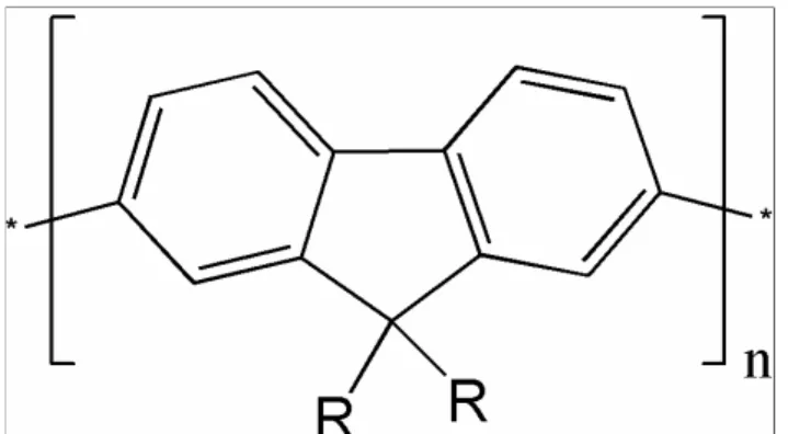
After the discovery of the electroluminescence of organic compounds by Bernanose in 1953, who performed studies on dyes including gonacrin, brilliant acridine orange E and carbazole, many different classes of conjugated polymers like poly(p-phenylene) (PPP), polythiophene (PT) and polyfluorene (PF) have been synthesized, investigated and further developed for applications in solid-state lighting till date [18 36]. Although PPPs offer a number of benefits like chemical stability and large bandgap for blue light emission, there are certain drawbacks such as the insolubility of PPPs in common organic solvents, causing a significant reduction in the processability of the polymer. The solubility of PPPs has been increased by introduction of bulky alkyl chains to the phenylene units; however these chains lead to the destruction of conjugation, because of the enforcement of steric strains. PFs, on the other hand are molecular compounds with pairs of phenylene rings locked into a coplanar arrangement by the carbon atom at the 9th position as shown in Fig. 2.1 [37]. Functionalization of the backbone at that particular C-9 position for enhancement of solubility causes no change in the high fluorescence quantum yields and high degree of brightness.
Figure 2.1. Chemical structure of a polyfluorene backbone with functional groups R attached at the 9th position.
On-going research has, however, shown, that PFs lack spectral stability which is verified by a change in the blue emission to a greenish-blue broad band emission. This is basically attributed to chemical structure changes in form of
9
keto defects by thermo-, photo- or electro-oxidative degradation. Another mechanism leading to significant changes in the emission properties of π-conjugated polymers is the physical aggregation observed especially in film form. Deposition of solutions of π-conjugated polymers by spin-coating or drop-casting onto solid substrates results in electronic coupling of polymer chains (interchain interaction), which is essential for charge carrier transport in the film state. The presence of interchain coupled states may induce an efficient energy transfer from higher energy intrachain singlet excitons to lower lying eigenstates that are delocalized over several polymer chains in intimate contact with each other through dispersive relaxation processes. In fact, the aggregate-induced depopulation of the initially excited intrachain excitons results in a red-
Figure 2.2. Energy-minimized 3D structure of cyclodextrin-threaded polyrotaxane with poly(para-phenylene) (β-CD-PPP) and its chemical structure[38].
10
shifted emission band, which is also associated with a significant reduction in the fluorescence quantum efficiency (ΦPL) in film state in the order of 50% [39].
To address this problem faced in films of conjugated polymers, which are essential for device applications, some researchers have developed various isolation techniques like rotaxanation (Fig. 2.2) [38], blending of various polymer structures and introduction of bulky dendrimer side groups to the polymer network [40]. These changes are supposed to reduce stacking interactions among molecules which may otherwise lead to significant quenching of the photoluminescence intensity in polymers.
Figure 2.3. Cartoon representation of the process flow for the reprecipitation method of polyfluorene with the chemical structure of the polymer given at the bottom.
11
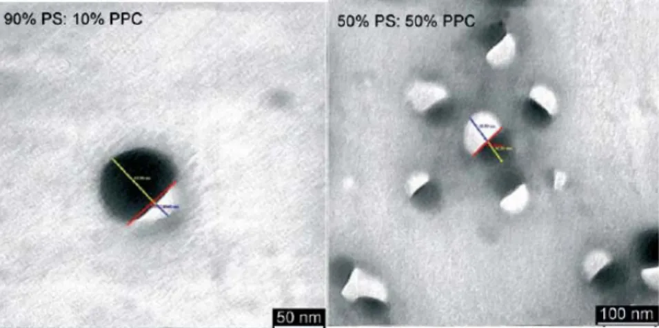
A recently newly developed approach for the processing of conjugated polymers for potential use in device applications is the formation of organic nanoparticles from π-conjugated polymers [41,42,43,44,45,46]. Various methods have been proposed for the formation of organic nanoparticles including mini-emulsion process, hydrothermal synthesis, and reprecipitation methods (Fig. 2.3) [42,43,44,45,46,47,48,49]. By making use of the mini-emulsion approach, Scherf and coworkers reported that polymer layers can possess improved performance in a multi-component phase-separated morphology. Adjustment of optical and electro-optical properties is achieved by blending two individually prepared nanoparticle dispersions of different copolymers. Nanoparticles, containing both copolymer components, were prepared by mixing first the copolymer solutions and then forming the micro-emulsion as is depicted in Fig. 2.4 [43]. Though in their study in 2003 Scherf and coworkers believed that the blend nanosphere was composed of two randomly mixed polymers in each particle, it was later discovered that these particles were in fact two-component phase-separated particles with each side consisting of a different polymer as revealed by TEM images given in Fig. 2.5 [50]. In this method a water-immiscible solvent is used for the stock solution preparation of the copolymers. Also, the use of a surfactant is required by which the formation of the nanoparticles is stabilized as illustrated in Fig. 2.4 below.
12
Figure 2.4. a) Preparation of the solid polymer nanoparticle dispersion in water. b) Polymer blend preparation from a dispersion containing nanoparticles of two different polymers, or by using dispersions that contain both polymers in each individual nanoparticle [43].
Figure 2.5. TEM images of different biphasic blend particles with percentages of the amounts employed in the preparation given. The particles are deposited on a carbon-coated copper grid and left to dry under air. The samples are not further labeled or stained [50].
This approach allows for the preparation of novel nanoscale structures to be further processed as thin polymer films with novel optical properties.
Among the above listed methods, especially attractive is the reprecipitation method, because of its simplicity and versatility [39]. This method is applied by reprecipitation of a polymer solution into a poor solvent such as water under sonication, followed by vacuum evaporation of the good solvent inside the dispersion [48]. This method was first developed by Kasai et al., who also performed studies revealing the size-dependent optical properties of perylene nanoparticles. Depending on decreasing diameters of the particles, they observed blue-shifts in both the absorption and the fluorescence spectra related to the shortened conjugation length of particles varying from diameters of hundreds to tens of nanometers. The proposed mechanism for the increased
13
bandgap was a change in lattice state resulting from an increase in surface area, which reduces the Coulombic interactions between molecules [48].
Polymer nanoparticles are found to exhibit size-dependent properties as has been stated by Kurokawa and coworkers who have recorded blue-shifting absorption and emission spectra as the nanoparticle diameters were reduced from 420 to 40 nm. This observation was explained by a difference in polymer conformations and spatial arrangements.Also a lattice softening of the nanoparticles is believed to be responsible for the size-dependent properties in poly(3-[2-(N-dodecylcarbamoyloxy)ethyl]-thiophene-2,5-diyl) (P3DDUT) nanoparticles as is demonstrated in Fig. 2.6 [44,48].
14
Figure 2.6. (a) Structural formula of P3DDUT, (b-g) SEM images of nanoparticles prepared by reprecipitation method and dynamic light scattering (DLS) size distributions, (b,e) ) 0.1 wt.-% P3DDUT/THF at 20ºC, (c,f) 1.0 wt.-% P3DDUT/THF at 20ºC, (d,g) 1.0 wt.-% P3DDUT/THF at 80ºC [48].
Figure 2.7. (a) Absorption and (b) fluorescence spectra of P3DDUT nanoparticles, with various mean diameters, dispersed in water [44].
Another study conducted by McNeill and coworkers includes the preparation and characterization of nanoparticles formed by the reprecipitation of polymer poly(9,9-dioctylfluorene) (PFO), [{9,9-dioctyl-2,7-divinylene-fluorenylene}-alt-co-{2-methoxy-5-(2-ethylhexyloxy)-1,4-phenylene}] (PFPV) and poly[2-methoxy-5-(2-ethylhexyloxy)-1,4-phenylenevinylene] (MEH-PPV), recording a quantum yield of 10% [49]. They report a blue-shift for the absorption spectra but a red-shift for the fluorescence spectra of the nanoparticle dispersions of all three polymers with respect to their THF solutions. Fig. 2.8 is a nice illustration of the changes inabsorption and fluorescence spectra of nanoparticle dispersions versus solutions of these polymers, which are similar to previous observations of blue-shift in absorption spectra but the reverse effect with a red-shift in fluorescence spectra compared to other groups.
15
Figure 2.8. (a) Normalized absorption and (b) normalized fluorescence spectra of conjugated polymer nanoparticles (solid line) compared to polymers in THF solutions (dashed line). (c) Photo of various polymer nanoparticle dispersions under UV radiation [49].
These results reveal the compact conformation that causes increased interactions between polymer chains. The fluorescence quantum yield for the PFPV nanoparticles suspended in water is found to be 0.1.
16
Chapter 3
Semiconductor Nanocrystals
The development of synthesis methods to produce semiconducting colloidal quantum dots (QDs) led to an immense growth in research in this field over the past several decades because of the exciting optical and electrical properties of these artificial crystals [51,52,53]. The exploration of various electro-optical features of these nanocrystals (NCs) further induced the rapid expansion of research on the fundamental physics of these nanostructures. For example, one of the defining features of these semiconducting nanocrystals is the quantum size effect, which is a phenomenon caused by the comparable spatial extent of the electronic wavefunction with respect to the particle size, typically in the order of several nanometers [51]. This effect was discovered in the 80s simultaneously in the United States and Russia [54,55]. Consisting of only a few hundred to a few thousand atoms, QDs are typically composed of group II-VI, III-V and IV-VI elements, which allow for the adjustment of the desired emission wavelengths spanning a wide range depending on the type of elements used and the targeted size. Specific types of nanocrystals include CdS, CdSe (Fig. 3.1), ZnS, CdTe, PbS, PbSe, Si and Ge constituting the class of only core nanocrystals. Different from these core structures, there have also been synthesized core/shell nanocrystals such as CdSe/ZnS and CdTe/CdS in which the shell has a wider bandgap [56,57]. This serves for the surface passivation
17
and, as a result, leads to higher emission rates. The increased emission achieved by using these additional shell structures is a consequence of the charge carrier confinement inside the nanocrystals.
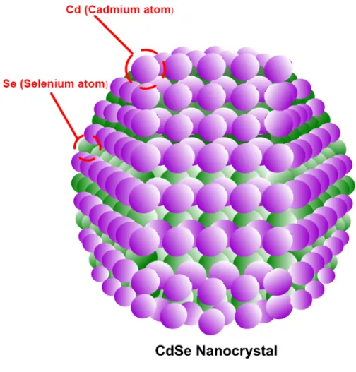
Figure 3.1. Wurtzite crystal structure of a CdSe quantum dot, where purple spheres indicate cadmium atoms and green ones selenium atoms.
Ongoing research makes important progress towards finding new, environment-friendly experimental routes and compounds for quantum dot formation, development of synthesis techniques for better size control and monodispersity, and the integration of these quantum dots into novel structures via surface functionalization (ligand exchange) [53]. Alternative, more environment-friendly synthetic routes have been developed in the recent years for which the
18
synthesis of water-soluble CdTe NCs can be listed as a nice example compared to its CdSe-like counterparts made by organometallic chemical methods [53]. Of particular interest in this study are these environmentally less harmful CdTe nanocrystals, which are composed of II-VI group atoms.
On the other extreme, in order to make these NCs more bio-applicable, there exist various methods to passivate biomolecules from the potential harms caused by toxic elements like cadmium. One of the methods used in literature is the exchange of the hydrophobic TOPO surface of CdSe/ZnS with a bifunctional molecule that is hydrophilic on one end and binds to ZnS on the other end [53]. For this purpose, one may use thiol (-SH) groups as one end for the ZnS binding while a carboxyl (-COOH) group can be used as the hydrophilic binding group. Very commonly used molecules for these applications are mercaptoacetic acid or mercatopropionic acid [58,59,60]. Unfortunately, the –SH-ZnS bonds are not as stable as –SH-Au bonds; as a result, these NCs start to precipitate in solution after certain treatment conditions including varying pH. A more difficult but stable chemical route towards the synthesis of biocompatible NCs is the silica capping of CdSe/ZnS NCs as is illustrated in Fig. 3.2 [61,62,63].
Figure 3.2. (a) Cross-sectional view of a silica shell capped CdSe/ZnS nanocrystal, and (b) chemical compounds used for the silanization of NCs. The outer surface of the silica shell is further functionalized with phosphonate and thiol groups [53].
19
Further stabilization of these particles is achieved by surface fuctionalization via various groups that are either negatively or positively charged like phosphonate or ammonium groups [64]. Thereby, particles carry a net charge on their surface, which prevents particle agglomeration in a long term. An even simpler method, however, is the adsorption of biocompatible polymers onto the NC surface through either recognizing head groups or electrostatic interactions between the capping layer of the NCs and the polymer molecules [65]. This can be achieved by the use of polyelectrolyte molecules like poly(allyl amine) (PAA) or polystyrene sulfonate (PSS) depending on the positive or negative nature of the surface charge on the NCs.
3.1 Size and Color Tuning: The Quantum Size
Effect
It is worth noting that nanocrystals should be considered different from their bulk forms. In bulk form crystals exhibit more continuous-like energy bands (although the energy levels are indeed discretized due to the finitie size of the crystal). Energy levels, however, become more discrete when the quantum size effects come into play via reduction of crystal size to nanoscales, by which electron hole pairs are confined to quasi-zero dimensions [51]. The wavelength control of the emitted light resulting from the excitation of nanocrystals is mainly governed by two factors. The first one is the composition of the nanocrystal; the second is the size. Nanocrystals, which are also commonly termed as ‘artificial atoms’ owing to the resemblance of their discrete energy levels to that of atoms, exhibit highly tunable emission properties. The energy bandgap of nanocrystals can be very precisely set through variation of size during their synthesis. Analogous to a particle-in-a-box model, because of their small size, which is comparable to the de Broglie wavelength of charge carriers,
20
NCs form discrete quantum energy levels, in which free electrons and holes are trapped in all three dimensions. The more the dimensions of the quantum dot approach the de Broglie wavelength, the more energy is needed to confine the electron-hole within that small volume; as a result emission at shorter wavelengths is observed. The exciton binding energy is given by the following expression in (3.1). 2 2 2
8mr
n
E
n=
h
(3.1)The quantum size effect is the underlying reason for the blue-shifted emission for decreasing nanocrystal dimensions, i.e., for growing nanocrystal diameter we can clearly observe emission peaks towards the red end of the visible spectrum. Specifically, it has been recorded that CdSe/ZnS core/shell NCs emit from 490 to 620 nm, while PbSe and PbS this range changes from 850 nm to 2100 nm [66]. As one of the fascinating properties of NCs, it is thus possible to tune the emission wavelength by variations in size as well as the composition of the quantum dots during synthesis, which make NCs the material of choice for numerous applications. Nowadays NCs find use in optical device electronics like light emitting diodes, diode lasers, storage devices, photodetectors, photovoltaic solar cells, amplifiers, and biosensors [67,68,69,70,71,72].
3.2 CdTe Nanocrystal Synthesis
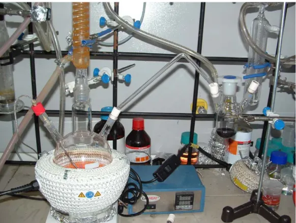
The water-soluble CdTe nanocrystals are synthesized in our laboratory. The synthetic route used for nanocrystal formation is as follows under the methodology of our collaborators’ work [73,74]. First, a solution containing 4.59 g Cd(ClO4)2 prepared into 0.2 L Milli-Q water (18.2 MΩ cm-1). Next, a
second solution containing 1.31 g of TGA is prepared in 0.3 L water. Both solutions are then mixed so that the total volume of the solution becomes 0.5 L.
21
Because a basic medium is required for the synthesis of CdTe NCs, the solution pH is set to 12 by drop-wise addition of ca. 30 mL of 1 M NaOH solution under continuous stirring. To prevent any oxidative reactions, the reaction flask is kept under Argon purge and stirring is continued throughout the reaction. In another flask, a 10 mL solution of 0.5 M H2SO4 and 15 mL of Milli-Q water are mixed.
This solution is further degassed for 20-30 min to ensure complete depletion of the inside oxygen content. In the next step, 0.8 g of Al2Te3 is measured in
another flask in the glove-box, because of the high tendency of this compound to oxidize under air conditions. To transport the measured Al2Te3 in a gaseous state
to the main flask again a continuous Ar flow is used, which carries the produced gas through the bridging glassware and should last for 30-40 min. The setup for nanocrystal synthesis in our laboratory is given in Fig. 3.2.1. To start gas formation, 10 mL of the previously prepared H2SO4 solution is taken with a
syringe, which is then slowly dropped into Al2Te3. Right after, the main solution
turns into red, then into dark red and finally to black. To finish up the preparation of the pre-cursors, we continue stirring further for 25 min and increase the Ar flow inside the flask. At this point there is no more need for the Al2Te3 line, which can be disconnected; instead a condenser is attached to the
main flask. Now, the main solution is heated up to 100 ºC and NCs start to grow when the solution begins to boil. Depending on the boiling time, as more atoms add to the nucleated crystal, the crystal size becomes bigger and accordingly the emission characteristics change.
22
Figure 3.2.1. A picture of CdTe nanocrystal synthesis setup. Precursors are produced in the main flask (left) and Al2Te3 source is activated in the small three-necked flask (right).
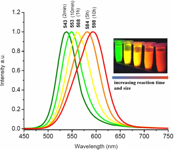
During the first minute of reaction time, the emission obtained from the NCs is blue, which then turns to green and upon further waiting finally to red if the solution is allowed to react for a sufficient time. The reaction is brought to a stop by rapidly cooling the mixture down to room temperature. For further removal of excess solvent and increase of NC concentration, vacuum evaporation may be used. Also, the synthesized colloidal quantum dots are cleaned from remaining impurities by simple filtering and are thereafter size-selectively precipitated by repetitive centrifugation steps. Through this procedure, it is possible to synthesize highly efficient, negatively charged CdTe NCs. Fig. 3.2.2 is a plot of the light emission obtained from variously sized CdTe NCs upon UV illumination.
23
Figure 3.2.2. (onset) Normalized photoluminescence spectra of our CdTe NCs emitting at different wavelengths which correspond to different boiling durations. (inset) A photo of our CdTe nanocrystals emitting in different colors depending on the size distribution.
3.3 Measurement of Fluorescence Quantum
Efficiency
The fluorescence quantum efficiency (QE), also known as the fluorescence quantum yield, is a measure of a fluorophore of how much of the incident pump light is transformed into emitted light in photon counts [75]. In other words, it is the ratio of the number of emitted photons to the number of absorbed photons.
24
To make QE measurements properly, there is a need for a specific reference material with exactly known quantum efficiency value in a certain solvent. Usually, the well known dye Rhodamine 6G in pure ethanol is well suited for NC QE measurements. The highest range of fluorescence quantum efficiency recorded in literature for nanocrystals is around 80%. The excitation wavelength of the fluorophores is chosen at the intersection point of the absorbances of the NCs and the reference dye. At this intersection wavelength both fluorophores are excited using a fluorometer, after which follows a fluorescence emission comparison. The whole underlying area under the fluorescence curve is integrated for both species, where the x-axis is converted from wavelength to energy. Using the efficiency of 95 % for Rhodamine, a relative fluorescence quantum efficiency value is calculated for nanocrystals. Better and more reliable results are obtained if these measurements are taken for multiple NC concentrations and afterwards a best-line is plotted. The fluorescence quantum efficiency of CdTe nanocrystals emitting at 537 nm is typically around 21 % in water.
25
Chapter 4
Fundamentals of Surface Plasmons
Early observation of the optical effects caused by plasmonic structures date back to the 4th century AD, when Romans utilized the famous historical metal nanoparticle stained cup, the Lycurgus, which is currently exhibited at the British Museum [27].
Figure 4.1. (Left) The Lycurgus cup when light is shine from the outside (reflection), and (right) when light is shine from the inside of the cup (absorption).
26
Under normal lighting conditions from the outside, the stained cup appears as green, while when illuminated from the inside this cup becomes red in color. This optical phenomenon known as surface plasmon resonance, which was unintentionally discovered at these early times, is effective at structure sizes around 20 times smaller than the wavelength of incident light. Besides the size of the material, what causes this effect is also the material used inside this cup. When light is incident on the cup, the metal and light strongly interact. Free electrons present in the metal structure start to strongly oscillate, generating a screening field so that light cannot pass through but is reflected. This strong oscillation can only be generated at certain frequencies, which are called the material’s plasmon resonance frequency. At these specific frequencies light is highly absorbed and reflected, which gives the metal cup its characteristic properties depending on the metal structure size.
Surface plasmons are the collective oscillations of electrons arising at the interface between a dielectric and the conductor metal. There essentially exist two types of plasmons, the localized plasmons (LP) and the surface propagating plasmons (SP) as is illustrated in Fig. 4.2 [76].
27
Figure 4.2. Schematic representation of surface propagating and localized plasmons on nanostructured gold surfaces [76].
This terminology may cause confusion, as all plasmons are generated at the surface of metals. The term LP is simply used when surface plasmons are trapped within confined metal nanostructures like voids or spheres and the latter term SP refers to the generation of freely propagating electromagnetic surface waves along a continuous metal surface [77]. Resulting electromagnetic fields can be calculated by solving the Maxwell equations with corresponding boundary conditions. In this work, we investigate optical behavior in hybrid systems by making use of LPs, which enable a wide range of practical applications including light guiding and manipulation at the nanoscale, biosensing at the single molecule level, enhanced optical transmission and high resolution optical imaging like surface-enhanced Raman spectroscopy, and fluorescence emission enhancement.
4.1 Optical Properties of Metals
One of the first scientific reports of surface plasmons dates back to the beginning of the 20th century. In 1904, Maxwell Garnett observed bright colors in stained glasses (metal stained) and described their optical behavior in terms of the newly developed Drude model for metals and the electromagnetic properties of small spherical metal particles as derived by Lord Rayleigh [78]. In the upcoming years in 1908, Mie makes a great contribution to this field by developing his widely used theory of light scattering by spherical particles, which elucidates the scattering and absorption characteristics of spherical particles at various sizes [79]. In 1956, David Pines conducts theoretical calculations to explain the energy losses of fast electrons passing through metals and ascribes the electron energy reduction to collective oscillations of free electrons in the metal [79]. At this time, these oscillations are named as ‘plasmons’. Later studies revealed that the
28
plasmon modes generated by metal particles reside at the surface of metals. One year later, the coupled oscillations of bound electrons inside the metal and light were termed as ‘polaritons’ [78]. Although up to this point surface plasmons have been extensively studied and understood, the relation to its optical properties have not been understood till 1970. As more and more developments contributed in the following years to this field, there has been a gradual transition from the fundamental studies to more application driven research. One of the major contributions made in this field was accomplished by Fleischmann and coworkers, who observed strong Raman signals from pyridine molecules in close vicinity to rough Ag surfaces [79]. The Raman scattering signal was enhanced by the nearby electromagnetic field at the silver surface due to the surface plasmons. This discovery further opened up horizons in the currently well-established field of surface enhanced Raman scattering (SERS) [80].
As a first approximation, a metal can be viewed as an isotropic medium with a dielectric constant denoted by ε, a permeability µ and a conductivity σ. Using these parameters the Maxwell equations take the following form,
∇
•
Η
=
0
(4.1)ε
ρ
= Ε • ∇ (4.2) =0 ∂ Η ∂ + Ε × ∇ tμ
(4.3)=
Ε
∂
Ε
∂
−
Η
×
∇
ε
σ
t
(4.4)which can be further transformed to give useful information about the optical properties of the metal particles. Using (4.3) and (4.4) and taking the divergence of (4.4), one obtains,
29
ρ
ρ
/τ 0 t e− = (4.5) where τ =ε/σ . Since the conductivity of gold is very large, the relaxation time τ becomes a relatively small value, which is around 10-12 s [81]. Within anapproximate approach it is realistic to take therefore ρ to be zero. After rearranging expressions (4.3) and (4.4) and by considering the planewave solution to Maxwell’s equations, one gets,
Ε=Ε0exp(ikˆ•x−i
ω
t) (4.6) for which then the wave equation for the metal can be written as∇2Ε+ 2Ε=0 k (4.7) where 2 2 ( ) ω σ ε μ ω i
k = + . Now, the refractive index can be defined by the following complex expression;
nˆ=n+i
κ
=εμ
(4.8) where κ is the extinction coefficient. The following expressions relate the dielectric constant and the refractive index to each other:2 1 2 2 2 1
ε
ε
ε
+ + = n and 2 1 2 2 2 1ε
ε
ε
κ
= + − (4.9) for complexε
ˆ
=
ε
1+
ε
2. From here the planewave equation can be re-written as0exp( 2 )exp[ (2 i t)] nx i x
ω
λ
π
λ
πκ
− − Ε = Ε (4.10)The first exponential in (4.10), which is real, stands for the absorption of the light, while the second part, which is complex, represents the oscillatory part of the wave. At this point, one should define the penetration depth of a material,
30
which is the depth light can travel inside a material where the electric field strength reduces to 1/e of its initial value. For visible frequencies, this value is found to be approximately 40 nm for gold. The expression for the penetration depth is given as
δ
(
λ
)
=
λ
(
2
πκ
(
λ
))
(4.11) Up to now, the parameters defining a material were considered to be constants; however, in reality they are not. The properties are highly dependent on the wavelength and thus have to be considered while performing optical calculations. The dielectric constant is a measure of how electrons in a medium respond to an optical field. These electrons can be either free or bound electrons as it is the case for a metal or a dielectric material, respectively. The oscillatory behavior of the applied optical field can be described in terms of simple harmonic motion, as it done via the Lorentz and Drude models for dielectric materials and metals, repectively [79].
m
x
&&
+
b
x
&
+
Kx
=
e
Ε
(4.12) where m and e are the electron mass and charge, b is the damping coefficient standing for the energy loss due to scattering events, K is the spring constant and E is the electric field. For a metal, the conduction band is partially filled with free electrons, which allows for interband transitions at low energies so that it is possible to assume the spring constant to be 0. Laborious calculations using expression (4.12), lead to the desired expressions for the real and complex parts of the dielectric constant, which are given as follows1
1
(
ω
2γ
2)
ω
ε
=
−
p+
and ) ( 2 2 2 2ω
ω
γ
γ
ω
ε
+ = p (4.13)where ωp is defined as the plasma frequency given by 0 2
ε
ω
p =ne m , and mb / =
γ . The plasma frequency is defined as the frequency at which the dielectric constant components are zero so that there are no TEM modes in the
31
Figure 4.1.1. Schematic representation of electric field which is created by an incident wave and corresponding shift of electron cloud resulting in a plasmon resonance of the particle [82].
material and the wave is purely longitudinal, which corresponds to collective oscillations of the electrons in the direction of wave propagation. When a metal is radiated with light, the free electrons inside the metal will start to oscillate at the resonance frequency and generate a charge distribution within the metal, which will in turn form an electric field to reverse this effect and restore the initial neutral charge distribution. Fig. 4.1.1 depicts the polarization on the particle (with a sinusoidally varying electric field) and a restoring force generated due to the Coulomb attraction force between the fixed positively charged lattice and the conduction electrons [82]. The generated strong electric field inside the metal is an exponential function, which therefore readily decays to zero values at short distances. This effect is well observed for very small particles up to the penetration depth. When larger particle sizes are used, the metal behaves as a perfect reflector or even at lower frequencies, when the skin depth is reduced reflection becomes a dominant phenomenon. Although the Drude model is very effective in approximating optical properties of metals, it is not sufficient for metals like gold and silver due to complex interband transitions. Therefore, a model which uses both the Lorentz and the Drude models is necessary.
32
The surface plasmon resonance frequency of a metal nanoparticle is a property that strongly depends on the material of which it is composed. Various studies have shown that Al, Pb and Hg have SPR frequencies corresponding to the UV region, while Ag and Au NPs exhibit resonance frequencies towards the visible region. For this reason the latter two metals are very commonly used in applications including emission enhancement via plasmon-exciton interactions. Recent studies however have revealed that also Al NPs are very good candidates for the radiative power enhancement of intrinsic emission from bio-emitters like various peptides which are very commonly found in organisms [83]. The classical surface plasmon resonance is given in equation (4.14)
3 12 0 2
)
4
(
s er
m
e
π
ε
ω
=
(4.14)where ε0 is the vacuum permittivity, me is the effective mass, and rs is the radius
of the sphere [84]. As can be seen from the equation, nanoparticle size is inversely proportional to the resonance frequency.
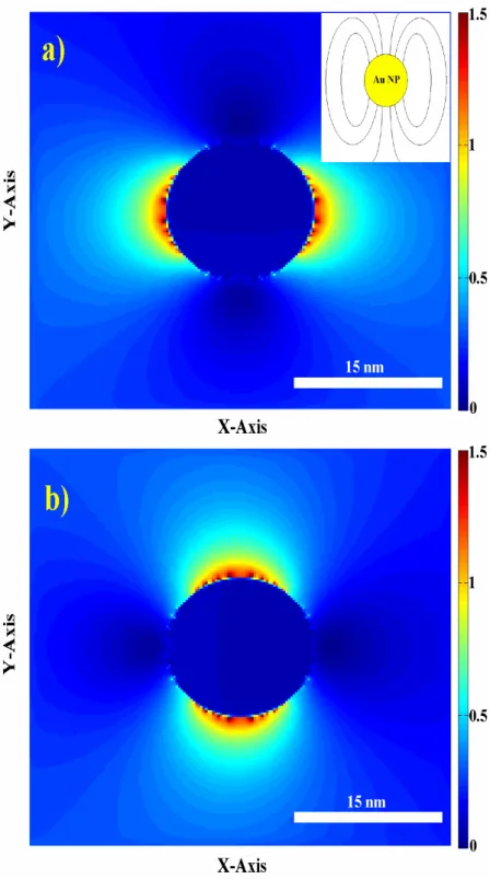
Finite difference time domain (FDTD) calculations made by using the commercially available simulation program (Lumerical Solutions Inc., Vancouver, Canada) reveal the effect of incident radiation on the near-field enhancement around the metal nanoparticle. The electric field intensity is maximized on the metal surface at the direction of polarization of the incident radiation and decays at very small distances as depicted in Fig. 4.1.2.
![Figure 2.2. Energy-minimized 3D structure of cyclodextrin-threaded polyrotaxane with poly(para-phenylene) (β-CD-PPP) and its chemical structure[38]](https://thumb-eu.123doks.com/thumbv2/9libnet/5911499.122522/27.892.184.808.589.1033/minimized-structure-cyclodextrin-threaded-polyrotaxane-phenylene-chemical-structure.webp)

![Figure 4.1.1. Schematic representation of electric field which is created by an incident wave and corresponding shift of electron cloud resulting in a plasmon resonance of the particle [82]](https://thumb-eu.123doks.com/thumbv2/9libnet/5911499.122522/49.892.196.770.223.460/schematic-representation-electric-incident-corresponding-electron-resulting-resonance.webp)