1
OA-2
Fabrication
of 100 nm
pMOSFETs
with
Hybrid
AFM
/
STM
Lit
Hyongsok T.
Soh, Kathryn Wilder, Abdullah Atalar and Calvin
F.
Quate
E. L. Ginzton Laboratory, Stanford University, Stanford, CA 94305-4085, U.S.A.I n t r o d u c t i o n
Scanning probe lithography (SPL) is an emerging area of research in which the scanning tunneling microscope (STM) or atomic force microscope (AFM) is used to pattern nanometer-scale features. Four factors will dictate the viability of SPL as a patterning technology for the semiconductor industry: 1) resolution, 2) alignment accuracy, 3) reliability, and 4) throughput. We present a new SPL technique-a hybrid between the AFM and STM-
to address these issues. We demonstrate its capabilities and its compatibility with semiconductor processing by fabricating a pMOSFET with an effective channel length (L,ff) of 100 nm and report the device characteristics.
Hybrid AFM / STM Lithography System
The Hybrid AFM / STM lithography system (Fig. 1) combines the key features of the AFM and STM by incorporating two independent feedback loops (1). One loop keeps the tip on the surface of the resist and maintains a constant force (typically 10 nN). This eliminates the problems of tip penetration into the resist while traveling over topography and minimizes the electron-beam spreading that limits the resolution of STM lithography (2). The second feedback loop maintains a constant field emission current. Without this feedback loop, any variation in resist thickness (encountered over topography) or any change in tip shape would alter the dose of electrons delivered to the resist.
Process Integration of the pMOSFETs
We used “mix and match” lithography to fabricate the pMOSFET where the gate level is patterned with Hybrid AFM / STM lithography in air. LOCOS isolation (field oxide = 450 nm) is performed followed by
an
arsenic channel implant (100 KeV, 1 x l O I 3 /cm2). The gate oxide thickness is 5.7 nm and the polysilicon thickness is 100nm. Before gate patterning, the poly is implanted with BF2, followed by an RTA (10 sec, N2, lO5O0C) to electrically activate the dopants. The poly must be conductive for Hybrid AFM / STM lithography. 50 nm of low temperature oxide (LTO) is deposited and patterned by photolithography.
Fig 2a shows the transistor structure after the gate pad formation.
A negative-tone e-beam resist (SAL-601) diluted with Microposit Thinner Type A is used. The resist is nominally
60 nm thick after spin on. The resist is first imaged with the AFM in contact mode to precisely locate the position where the gate will be written. The image is then imported into the lithography software, which controls the path and the speed o f the tip. The closed loop feedback used in our scanner (Park Scientific Instruments Autoprobe M5) eliminates hysteresis and enables alignment accuracy of a few nanometers. A Ti-coated silicon tip is used to expose the resist (Fig. 2b). After development (Fig 2c), the poly is
Fig 2 illustrates the gate patterning steps.
etched in SFg/Freon 115 plasma where the LTO protects the gate pad and the SAL-601 masks the gate (Fig 2d).
The resist thickness variation over the LOCOS topography caused by planarization is shown in Fig. 3a and 3b. The thickness changes abruptly from less than 30 nm to more than 90 nm within a micron. The voltage and field- emitted current during exposure are plotted in Fig 3c. The voltage required to maintain 0.05 nA ranges from 22 V to 8 1 V. Note that a change in voltage, aV/at, generates a displacement current proportional to the capacitance between the probe and the sample. This parasitic tip-sample capacitance was reduced below 600
fF,
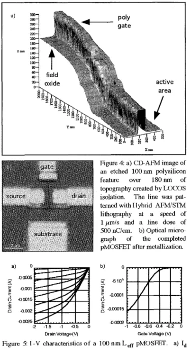
which allowed patterning of continuous sub- 100-nm features over the 180- nm of topography in a single pass. Fig. 4a is a critical dimension AFM (CD-AFM) (3) image of a 100-nm etched poly feature across the transition region from the field oxide to the active area. The scan speed was 1 w m / s and the line dose was 500 nC/cm. We have fabricated pMOSFETs with Lphysical ranging from 61 nm to 170 nm.After gate lithography, a 35 nm oxide spacer is formed by LTO deposition and anisotropic RIE. Shallow source/ drain junctions are created by BF2 implantation (10 KeV, l x 1 0 1 5 / c m 2 ) . The final processing steps are: LTO passivation, RTA (10 sec, N2, 105O0C), furnace anneal (30 min, Nz, SOO0C), contact photolithography, metallization, and a forming gas anneal. An optical micrograph of the finished structure is shown in Fig. 4b.
Device Results
The characteristics of a device with L,ff o f 100 nm are shown in Fig 5a and 5b. A saturation current drive of 0.244 mA/pm and saturated transconductance (gm) of 154 mS/mm
are achieved at -2 V. The threshold voltage (V,) is -0.41 V.
Devices with smaller gate lengths show excessive leakage. The Vt rolloff, maximum saturated current (Idmax,), and g, as a function of channel length are plotted in Fig. 6a, b, and c, respectively. Transistors with gate lengths larger than 170 nm were patterned with photolithography to show the trend as a function of gate length.
C o n c l u s i o n s
We have demonstrated the capability of Hybrid AFM I STM lithography to fabricate pMOSFETs with Lphysical ranging from 61 nm to 170 nm and have shown the system’s compatibility with semiconductor processing. Device characteristics for Leff of 100 nm are presented. This new SPL technique is capable of sub-100-nm resolution and nanometer-scale alignment accuracy with reproducible patterning over significant topography. This system can be extended to high speed and multiple probe patterning and may provide an alternative technology for critical dimension patterning of 100-nm feature sizes and beyond.
References
(1) K. Wilder, H.T. Soh, A. Atalar, C.F. (&ate, “The hybrid AFM I STM lithography system,” unpublished.
(2) C.R.K. Marian, E.A. Dobisz, R.J. Colton, “Lithographic studies of an e-beam resist in a vacuum scanning tunneling microscope,” J. Vac. Sci. Technol. A, 8,4,3563-3569 (1990).
( 3 ) Y. Martin, H.K. Wickramasinghe, “Method for imaging sidewalls by atomic force microscopy,” Appl. Phys. Lett., 64,
19,2498-2500 (1994).
FORCE FEEDBACK _ _ _ _ _ _ _ _ _ _ _ _ _ _ _ _ _ - -
L I
Figure 1: Schematic diagram of the Hybrid AFM I STM lithogra- phy system incorporating dual feedback loops.
Figure 2: Schematic of the gate patterning procedure: a) LTO gate pad is photolithographically defined; b) SAL601 resist is spun and Hybrid AFM I STM lithography is performed; c) Exposed gate remains after development; d) Poly is etched by NE.
0.45 0.35 0.25
g
3 0.15 -3 P 0.05-
-0.05 Posltion@rn)Figure 3: a) Poly and resist topography created by LOCOS
isolation; b) Resist thickness variation as a function of position; c) Current and voltage during Hybrid AFM I STM lithography.
a) 0
-
4.m 5 g 0.001 8 -0.W15 P 0 0.002 -0.0025-
._ 4 -1.5 -1 -0.5 0 DrainVdtage(V)Figure 4: a) CDAFM image of
an etched 100nm plysilicon feature over 180nm of topography created by LOCOS
isolation. The line was p a - terned with Hybrid AFMISTM lithography at a speed of
l p d s and a line dose of
500 nC/cm. b) Optical micro- graph of the completed pMOSFET after metallization.
Gate Vdtage (V)
Figure 5 I -V characteristics of a 100 nm L, pMOSFET. a) Id
versus V, where V, was varied from 0 V to - 2 V in steps of -0.25
V. b) I, versus V, at a Vd of -0.1 V showing V, to be -0.41 V . a ) -0.25 -0.35 ?-.. 2. -0.45 -0.55 -0.65 0 1 2 3 4 b ) 2 E -2 g , -1 E - 4 -5 0 1 2 3 4
Leff W W Len fpm) Leff m)
Figure 6: Electrical characteristics as a function of LeK for l@pm- wide devices: a) Threshold voltage roll-off; b) Maximum saturated current; c) Maximum saturated transconductance.
Acknowledgments: This work was supported by DARPA and
NSF. The authors thank AMD, PSI, K. Perkins at NRL, and M. McCord and the CIS staff at Stanford University.