GROWTH AND CHARACTERIZATION OF
BORON NITRIDE THIN FILMS AND
NANOSTRUCTURES USING ATOMIC
LAYER DEPOSITION
A THESIS
SUBMITTED TO MATERIALS SCIENCE AND NANOTECHNOLOGY PROGRAM
OF THE GRADUATE SCHOOL OF ENGINEERING AND SCIENCE OF BILKENT UNIVERSITY
IN PARTIAL FULFILLMENT OF THE REQUIREMENTS FOR THE DEGREE OF
MASTER OF SCIENCE
By
Ali Haider
August, 2014
I certify that I have read this thesis and that in my opinion it is fully adequate, in scope and in quality, as a thesis for the degree of Master of Science.
Assist. Prof. Dr. Necmi Bıyıklı (Supervisor)
I certify that I have read this thesis and that in my opinion it is fully adequate, in scope and in quality, as a thesis for the degree of Master of Science.
Assist. Prof. Ferdi Karadaş
I certify that I have read this thesis and that in my opinion it is fully adequate, in scope and in quality, as a thesis for the degree of Master of Science.
Assoc. Prof. Tamer Uyar
Approved for the Graduate School of Engineering and Science:
Prof. Dr. Levent Onural Director of Graduate School
i
ABSTRACT
GROWTH AND CHARACTERIZATION OF BORON
NITRIDE THIN FILMS AND NANOSTRUCTURES
USING ATOMIC LAYER DEPOSITION
Ali Haider
M.S. in Materials Science and Nanotechnology Supervisor: Assist. Prof. Dr. Necmi Biyikli
August, 2014
Being a member of III-nitride family, boron nitride (BN) and its nanostructures have recently attracted a lot of attention, mainly due to their distinctive and superior material properties, including wide band gap, high-temperature stability, high oxidation and corrosion resistance, as well as high thermal conductivity. This versatile material has found applications in UV emission, lubrication, composite reinforcement, gas adsorption, cosmetics, and thermal management. For modern electronic applications, it is imperative to obtain high quality BN films on large area substrates with a controlled thickness in order to fulfill the entire spectrum of hBN applications. Also, a facile method such as atomic layer deposition (ALD) using non halide precursors is necessary to obtain BN films at low temperatures compliant with the standards in terms of having nontoxic byproducts. ALD is a special case of chemical vapor deposition (CVD), in which two or more precursors are sequentially exposed to substrate surface separated by purging periods. In comparison with other thin film growth methods, hall mark of ALD is self limiting growth mechanism which enables deposition of highly uniform and conformal thin films with sub-angstrom thickness control. The precise and conformal layer by layer growth of ALD can be exploited to achieve growth of BN hollow nanofibers (HNFs) on high aspect ratio electrospun polymer nanofibrous templates. BN HNFs fabricated by combination of ALD and electrospinning can be utilized to address and solve important constraints associated with previous methods of fabrication such as
ii
severe preparation conditions, limited control over morphology, and low purity of the resulting BN HNFs.
In this thesis, we report on the controlled deposition of BN films and its nanostructures with the use of a hollow-cathode plasma source integrated (HCPA-ALD) reactor and present detailed materials characterization results of deposited thin films and fabricated nanostructures. Depositions are carried out at low substrate temperatures (less than 450 °C) using sequential injection of non-halide triethylboron (TEB) and N2/H2 plasma as boron and nitrogen precursors,
respectively. The deposition process parameters such as pulse length of TEB and substrate temperature, as well as the influence of post-deposition annealing are studied. Moreover, another nonhalide alternative precursor named tris(dimethyl)amidoboron (TDMAB) was studied for deposition of BN films. Initial experiments were performed using TDMAB and N2/H2 plasma as boron
and nitrogen precursor. In addition to BN thin film growth studies, we report on electrospun polymeric nanofibrous template-based fabrication and characterization of AlN/BN bishell HNFs. Synthesized AlN/BN bishell HNFs were found to be polycrystalline with a hexagonal structure along with low-impurity content.
Keywords: Plasma-Enhanced Atomic Layer Deposition, Chemical Vapor
iii
ÖZET
BOR NİTRÜR İNCE FİLMLERİN VE
NANOYAPILARIN ATOMİK KATMAN BİRİKTİRME
YÖNTEMİ İLE BÜYÜTÜLMESİ VE
KARAKTERİZASYONU
Ali Haider
Malzeme Bilimi ve Nanoteknoloji, Yüksek Lisans Tez Yöneticisi: Yrd. Doç. Dr. Necmi Bıyıklı
Ağustos, 2014
III-nitrür ailesinin bir üyesi olarak, bor nitrür (BN) ve nanoyapıları geniş bant aralığı, yüksek-sıcaklık kararlılığı, ve yüksek oksitlenme ve korozyon direncinin yanısıra yüksek ısıl iletkenliği de içeren ayırt edici ve üstün malzeme özellikleri sayesinde yakın zamanda çokça dikkat çekmiştir. Bu çok yönlü malzeme UV emisyonu, yağlama, kompozit güçlendirme, gaz adsorpsiyonu, kozmetik, ve ısıl yönetimde uygulamalar bulmuştur. Modern elektronik uygulamalar için, hBN uygulamalarının tüm spektrumunu gerçekleştirmek amacı ile yüksek kaliteli ve kontrollü kalınlığa sahip BN filmlerin yüksek alanlı alttaşlar üzerine elde edilmesi gerekmektedir. Ayrıca, zehirli olmayan yan ürünler elde etmek açısından standartlarla uyumlu şekide düşük sıcaklıklarda BN filmler elde etmek için halojenür içermeyen öncü maddelerin kullanıldığı atomik katman biriktirme (AKB) gibi kolay bir metoda gerek duyulmaktadır. AKB iki ya da daha fazla öncü maddenin arındırma periyotları ile ayrılmış ardışık atımlarla alttaş yüzeyine gönderildiği özel bir kimyasal buhar biriktirme çeşididir. Diğer ince film büyütme metodları ile karşılaştırıldığında, AKB yönteminin ayırt edici özelliği muntazam ve konformal ince filmlerin angstrom-altı kalınlık kontrolü ile biriktirilmesine olanak sağlayan kendi kendini sınırlayan büyütme mekanizmasıdır. AKB yönteminin kesin ve konformal katman katman büyütme tarzı elektro lif çekimi yöntemi ile elde edilmiş yüksek boy/en oranına sahip polimer nanolif şablonlar üzerine BN oyuk nanoliflerin büyütülmesini
iv
gerçekleştirmek amacıyla da kullanılabilir. AKB ve elektro lif çekimi yöntemlerinin birlikte kullanılmasıyla üretilen BN oyuk nanolifler, ağır hazırlama koşulları, morfoloji üzerindeki sınırlı kontrol, ve elde edilen BN oyuk nanoliflerin düşük saflığı gibi, önceki üretim metodları ile ilgili önemli kısıtlamaları tanımlamak ve çözmek amacıyla kullanılabilir.
Bu tezde, BN filmlerin ve nanoyapıların oyuk katod plazma (OKP) kaynağı entegre edilmiş bir reaktörün kullanımıyla kontrollü bir şekilde büyütülmesini rapor etmekte, biriktirilen ince filmler ve üretilen nanoyapılar için detaylı malzeme karakterizasyon sonuçları sunmaktayız. Biriktirmeler düşük alttaş sıcaklıklarında (450 °C’den düşük), boron ve nitrojen öncü maddelerinin, sırasıyla halojenür olmayan trietilbor (TEB) ve N2/H2 plazmanın ardışık
enjeksiyonu kullanılarak gerçekleştirilmiştir. TEB’un atım süresi ve alttaş sıcaklığı gibi biriktirme süreç parametrelerinin yanısıra biriktirme sonrası tavlamanın etkileri de incelenmiştir. Ayrıca, BN filmlerin biriktirilmesi için tris(dimetil)amidobor (TDMAB) isimli, halojenür içermeyen diğer bir alternatif öncü madde araştırılmıştır. İlk deneyler, bor ve nitrojen öncü maddeleri olarak TDMAB ve N2/H2 plazmanın kullanılmasıyla gerçekleştirilmiştir. BN ince film
büyütme çalışmalarına ek olarak, AlN/BN iki kabuklu oyuk nanoliflerin elektro lif çekimi yöntemi ile elde edilmiş polimerik nanolif şablon-temelli üretimini ve karakterizasyonunu rapor etmekteyiz. Sentezlenen AlN/BN iki kabuklu oyuk nanoliflerin düşük safsızlık içeriği ile birlikte hegzagonal yapıya sahip ve çok taneli olduğu bulunmuştur.
Anahtar Kelimeler: Plazma-Destekli Atomik Katman Biriktirme, Kimyasal Buhar Biriktirme, Bor Nitrür, İnce Film, Nanolif
v
Acknowledgement
I would like to thank my supervisor, Prof. Dr. Necmi Biyikli, for the guidance, encouragement and advice he has provided throughout my time as his student. I want to express my gratitude to Cagla Ozgit-Akgun and Eda Cetinorgu-Goldenberg, for their continued support, help, and encouragement. I would also like to thank all engineers especially Semih Yasar, Mustafa Guler, and Enver Kahveci who contributed to my research experience and always helped me in enhancing my learning towards research equipments. Finally, I want to acknowledge Higher Education Commission of Pakistan (HEC) for Human resource development (HRD) fellowship for MS leading to PhD.
vi
Contents
Acknowledgement ... v
Contents ... vi
List of Figures ... viii
List of Tables ... xi
Chapter 1 ... 1
Introduction ... 1
1.1 Historical Background ... 1
1.2 An Overview on Atomic Layer Deposition ... 3
1.2.1 Mechanism ... 3
1.2.1.1 Ligand Exchange ... 4
1.2.1.2 Dissociation ... 5
1.2.1.3 Association ... 5
1.2.2 Factors Causing Saturation and Growth of Less than Monolayer per Cycle ... 6
1.2.3 Effect of Number of Cycles on GPC ... 7
1.2.4 Effect of Temperature on GPC ... 8
1.2.5 Growth Modes of ALD ... 10
1.2.6 ALD Window ... 11
1.2.7 Merits and Demerits of ALD and Comparison with Other Deposition Techniques ... 13
1.2.8 Classes of Precursors Utilized in ALD ... 14
1.2.9 Plasma vs. Thermal ALD ... 15
1.3 Motivation ... 18
1.4 Objectives ... 19
1.5 Literature overview ... 20
1.5.1 BN Thin Film Deposition Using HCPA-ALD Reactor ... 20
1.5.2 Fabrication of Aluminium Nitride (AlN)/BN Bishell Hollow Nanofibers (HNFs) ... 21
vii
Chapter 2 ... 23
Experimental Details ... 23
2.1 BN Deposition Using Sequential Injection of Triethylboron (TEB) and N2/H2 Plasma ... 23
2.2 BN Deposition using Sequential Injection of Tris(dimethyl)amidoboron (TDMAB) and N2/H2 Plasma ... 25
2.3 Post-growth Annealing of BN Thin Films ... 25
2.4 Fabrication of AlN/BN Bishell HNFs by Combination of Electrospinning and ALD ... 26
2.4.1 Electrospinning of Nylon Nanofibrous Sacrificial Templates ... 26
2.4.2 Atomic Layer Deposition of AlN ... 27
2.4.3 Removal of Sacrificial Nanofibrous Polymeric Templates ... 27
2.4.4 Low-Temperature Sequential CVD of BN ... 27
2.5 Characterization Methods ... 28
Chapter 3 ... 32
Results and Discussions... 32
3.1 BN Thin Films Growth Using Sequential Exposure of Triethylboron (TEB) and N2/H2 Plasma ... 32
3.1.1 Optimization of Growth Parameters ... 33
3.1.2 Characterization of BN Thin Films ... 36
3.1.2.1 Structural Characterization of BN Thin Film ... 36
3.1.2.2 Compositional Characterization ... 41
3.1.2.3 Morphological Characterization ... 43
3.1.2.4 Optical Characterization ... 45
3.2 Fabrication of AlN/BN Bishell HNFs by Electrospinning and ALD ... 48
3.2.1 characterization of AlN/BN Bishell HNFs ... 49
3.2.1.1 Morphological Characterization ... 49
3.2.1.2 Structural Characterization ... 51
3.2.1.3 Compositional Characterization ... 55
3.3 BN Deposition Using Sequential Exposures of Tris(dimethyl)amidoboron (TDMAB) and N2/H2 as Boron and Nitrogen Precursors. ... 57
Chapter 4 ... 61
Summary and Future Directions ... 61
viii
List of Figures
Figure 1.1: Schematic representation of an ALD cycle consisting of four steps. 4 Figure 1.2: (a) Ligand exchange reaction of the MLz reactant with surface “-a”,
releasing gaseous byproduct aL. (b) Ligand exchange can also occur between the surface group and adsorbed MLz-y complex. ... 5
Figure 1.3: (a) Dissociation of the MLz in surface M-Z sites. (b) Dissociation
may also occur between MZz-y complex and M-Z sites. ... 5
Figure 1.4: Association of the MLz complex onto the surface. (a) Association
can occur through formation of a coordinative bond between the central M ion and the surface, (b) or perhaps between the ligands and the surface. ... 6 Figure 1.5: Dependency of the GPC on the number of reaction cycles in different types of ALD processes: (a) linear growth, (b) substrate-enhanced growth, (c) substrate-inhibited growth of Type 1, and (d) substrate-inhibited growth of Type 2. ... 8 Figure 1.6: Variation of the GPC with the ALD processing temperature in the ALD window: (a) the GPC decreases with temperature, (b) the GPC is constant with temperature, (c) the GPC increases with temperature, and (d) the GPC first increases and then decreases with temperature. ... 9 Figure 1.7: Schematic illustration with increasing number of growth cycles of selected growth modes possible in ALD: (a) two-dimensional growth, (b) island growth, and (c) random deposition. ... 11 Figure 1.8: Effect of deposition temperature on the ALD growth rate. ... 12 Figure 1.9: Three main types of plasma reactor configurations for PEALD. (a) Radical-enhanced, (b) direct plasma, and (c) remote plasma configurations [40]. ... 17 Figure 2.1: Details regarding specific parts and their features of ALD system . 24 Figure 3.1: Effect of TEB dose on GPC at different temperatures. N2 and H2
ix
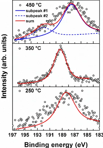
Figure 3.2: High-resolution B 1s scans obtained from Si surfaces, which have been exposed to 100 pulses of TEB at different temperatures. ... 35 Figure 3.3: (a) GIXRD patterns of ~47 and ~15 nm thick BN films deposited on Si (100) substrates at 450 and 350 C, respectively. (b) GIXRD pattern of the ~47 nm thick BN film deposited on Si (100) substrate at 450 C: annealed vs. as-deposited. (c) GIXRD patterns of ~47 and ~15 nm thick BN films deposited on Si (100) substrates at 450 and 350 C after annealing at 800 C for 30 min, respectively. ... 38 Figure 3.4: (a) Cross-sectional TEM image of AlN-capped ~90 nm thick BN thin film deposited at 450 °C on Si (100) substrate. (b) Cross-sectional HR-TEM image of the same sample. ... 39 Figure 3.5: (a) Elemental map of the AlN-capped ~90 nm thick BN thin film deposited on Si (100) substrate at 450 C. (b) SAED pattern of the same sample. ... 40 Figure 3.6: (a) Compositional depth profile of ~47 nm thick BN thin film deposited on Si (100) at 450 C. (b, c) High-resolution B 1s and N 1s scans of the same sample. Data were collected after 720 s of Ar ion etching. ... 42 Figure 3.7: SEM images of ~47 nm thick BN thin film deposited on Si (100) substrate at 450 C: (a) as-deposited, and (b) annealed. ... 44 Figure 3.8: (a) Surface morphologies of ~47 nm thick BN thin film deposited on Si (100) substrate at 450 C: (a), (b) as-deposited and (c), (d) annealed. ... 45 Figure 3.9: (a) Optical transmission, and (inset) absorption spectra of the ~47 nm thick BN thin film deposited on double side polished quartz. (b) Optical constants (refractive index and extinction coefficient) of the same sample ... 47 Figure 3.10: SEM images of electrospun Nylon 6,6 nanofiber templates having ~100 nm average fiber diameter. ... 49 Figure 3.11: SEM images of hollow AlN HNFs synthesized by depositing 200 cycles AlN on nylon 6,6 templates followed by calcination. ... 50 Figure 3.12: SEM images of AlN/BN bishell HNFs obtained after depositing BN on AlN fiber templates. ... 51
x
Figure 3.13: Bright field TEM image of (a) AlN hollow nanofibers synthesized by using nylon 6,6 template having an inner fiber diameter of ~100 nm with wall thickness of ~20nm (b) an individual AlN hollow nanofiber. ... 52 Figure 3.14: (a, b) Bright field TEM image of AlN/BN hollow nanofibers having an inner fiber diameter of ~100 nm with wall thickness of ~20 and ~35 nm of AlN and BN respectively, and (c) high resolution TEM images of BN nanoneedle like structure. ... 53 Figure 3.15: EDXs elemental mapping of AlN/BN bishell HNFs revealing elemental distribution of elements along the scanned area. ... 54 Figure 3.16: SAED pattern of AlN/BN bishell HNFs. ... 54 Figure 3.17: (a) B 1s and (b) N 1s high resolution XPS scans of AlN/BN HNFs based on nylon 6,6 templates. ... 56 Figure 3.18: HR-XPS scans of (a) and (b) B1s and N1s from bulk of as deposited film at 50 C, respectively, (c) and (d) B1s and N1s from bulk of annealed film at 900 C, respectively ... 59
xi
List of Tables
Table 1.1: Alternative names of ALD[5] ... 2 Table 1.2: Merits and demerits of ALD ... 13 Table 1.3: Comparison of ALD with other thin film deposition techniques [36]. ... 13 Table 3.1: Crystallite size calculation from Scherrer formula for BN films deposited at 450 and 350 C ... 39 Table 3.2: Refractive indices of the hBN films deposited on Si (100) substrates at different temperatures. ... 43 Table 3.3: Refractive indices of the hBN films deposited on Si (100) substrates at different temperatures. ... 47 Table 3.4: SAED results of AlN/BN bishell HNFs, comparison between measured and theoretical values of interplanar spacing (dhkl) with corresponding crystallographic planes. ... 55 Table 3.5: XPS survey scan results of AlN and AlN/BN bishell HNFs. ... 56 Table 3.6: measurement of thickness and refractive index of as deposited and annealed films ... 58 Table 3.7: XPS survey scan results from the surface and bulk of as deposited and annealed film. ... 59
1
Chapter 1
Introduction
1.1 Historical Background
Atomic layer deposition (ALD) is a special case of chemical vapor deposition technique where thin film deposition is achieved by dividing the reaction into two half cycles by sequential exposure of precursors separated with purge/evacuation periods. Hall marks of ALD are excellent surface coverage, highly conformal films, and precise thickness control at atomic scale owing to self-limiting reactions of precursors occurring at the substrate surface.
The origin of ALD dates back to 1970s. The credit of first realizing the principles of ALD is given to two different groups. The more acknowledged pioneer of ALD is Tuomo Suntola, who demonstrated ALD under the name of atomic layer epitaxy (ALE). The beginning of ALD dates back to a patent published in 1970s in which following processes were demonstrated: growth of ZnS by Zn/S precursors, growth of SnO2 by Sn/O2 precursors, and growth of
GaP by Ga/P precursors. The first commercial application of ALD has been demonstrated in manufacturing of thin film electroluminescent displays in 1980s [1].
2
On the other hand, less acknowledged pioneer of ALD is a research group in Soviet Union headed by Professor Aleskovskii. Shevjakov et al. first described the TiCl4/H2O process to grow layers of TiO2 and GeCl4/H2O process
to grow layers of GeO2 in the proceedings of a conference, which was organized
in 1965, and published in 1967. The Soviet Union researchers defined this technique as "molecular layering" [2].
Partly because of its history, and partly because of its unique properties, this technique has been referred with many different names. The current most widely used name is ALD, which dates back to early 1990s [3]. Plasma-enhanced ALE was first demonstrated in 1991 by De Keijser and Van Opdorp from Philips research laboratories in Eindhoven, Netherlands [4]. In their study, remote microwave-induced plasma was utilized to generate hydrogen radicals which were subsequently used for the growth of gallium arsenide. A major driving force for ALD is in the prospective seen in continuous scaling down of microelectronic devices by using ALD. Table 1.1 represents the alternative names and abbreviations of ALD which have been used in history instead of ALD.
Table 1.1: Alternative names of ALD[5]
Name Abbreviation
Atomic layer chemical vapor deposition ALCVD Atomic layer deposition ALD Atomic layer epitaxy ALE Atomic layer evaporation ALE Atomic layer growth ALG Chemical assembly
Digital layer epitaxy DLE Molecular deposition
Molecular lamination
Molecular layer epitaxy MLE Molecular layering ML
3
1.2 An Overview on Atomic Layer Deposition
ALD is a special type of CVD technique, in which unlike CVD, one reaction is splitted into two half reactions by exposing the reactants alternatively to the substrate surface, separated by an inert gas purge. As there are only limited number of reaction sites on the substrate after exposure of one precursor, one growth cycle will only deposit a fraction of a monolayer (sub-monolayer) of species. If both half reactions will be self-limiting, the growth will continue in a sequential manner to deposit a thin film with highly precise atomic-scale thickness control. This unique self terminating film growth mechanism also brings other advantages such as high conformality and high uniformity of the grown films [6].
1.2.1 Mechanism
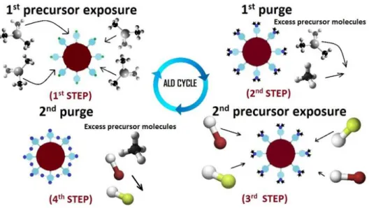
Figure 2.1 shows a schematic representation of a typical ALD cycle. Layer by layer material growth consists of following four steps:
(1) Exposure of first precursor, precursor adsorbs on reactive sites and reaction products are formed.
(2) Purge to evacuate the reactor from unreacted excess precursor molecules and gaseous reaction by-products.
(3) Exposure of second precursor, which reacts with the adsorbate to form a monolayer of desired material.
4
Figure 1.1: Schematic representation of an ALD cycle consisting of four steps.
As precursor molecules are exposed separately, each ALD cycle results in a monomolecular layer of the given precursor, which eventually becomes independent of the precursor exposure after saturation of the reactive surface sites. Therefore, ALD has the advantage of layer-by-layer self-limiting and ultimate conformal growth on high aspect ratio structures. After the completion of one cycle, substrate surface is returned back to its original state and is ready for the next cycle. As the amount of material deposited in one cycle remains constant after complete initial nucleation of the film, a film with desired thickness can simply be achieved by repeating the reaction cycles.
Three types of chemisorption reactions contribute to self-limiting reactions of ALD via compound reactants [5,7]:
1.2.1.1 Ligand Exchange
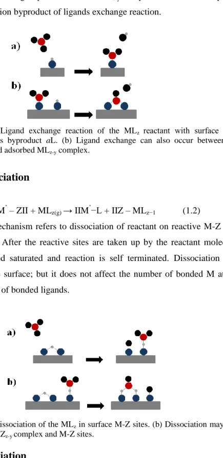
II – a + MLz(g) → II − MLz−1 + aL(g) (1.1)
Ligand exchange mechanism refers to splitting of a reactant molecule (MLz),
5
between the surface group and adsorbed MLz-y complex. A volatile compound
(aL) is the reaction byproduct of ligands exchange reaction.
Figure 1.2: (a) Ligand exchange reaction of the MLz reactant with surface “-a”,
releasing gaseous byproduct aL. (b) Ligand exchange can also occur between the surface group and adsorbed MLz-y complex.
1.2.1.2 Dissociation
IIM’ – ZII + MLz(g) → IIM’−L + IIZ – MLz−1 (1.2)
Dissociation mechanism refers to dissociation of reactant on reactive M-Z sites on the surface. After the reactive sites are taken up by the reactant molecule, surface is called saturated and reaction is self terminated. Dissociation may continue on the surface; but it does not affect the number of bonded M atoms and the number of bonded ligands.
Figure 1.3: (a) Dissociation of the MLz in surface M-Z sites. (b) Dissociation may also
occur between MZz-y complex and M-Z sites.
6
II + MLz(g) → II...MLz (1.3)
In association mechanism, adhering of reactant occur to reactive sites without releasing the legends. A coordinative bond is formed with the reactive surface sites.
Figure 1.4: Association of the MLz complex onto the surface. (a) Association can occur
through formation of a coordinative bond between the central M ion and the surface, (b) or perhaps between the ligands and the surface.
1.2.2 Factors Causing Saturation and Growth of Less than
Monolayer per Cycle
After one cycle is completed, a certain amount of material is deposited on the substrate surface called growth per cycle (GPC). Although there is a common misconception that one ALD cycle deposits one monolayer of material, the reality is different. GPC value is often less than a monolayer per cycle due to the effect known as “steric hindrance”. Highest GPC value correspond to completion of reaction by maxium number of surface sites reacting with the reactant through legend exchange. Usually a limited number of reactive sites are occupied by the reactants and steric hindrance terminates it [8,9]. The bulky legends block the remaining bonding sites and therefore the surface can be considered as full due to steric hindrance. The other reason of sub-monolayer saturation is the limited number of reactive sites in which the number of bonding sites is less than required to achieve a full ligand coverage [10,11].
7
1.2.3 Effect of Number of Cycles on GPC
The first ALD cycle exposes the reactants on the original substrate material, and the following cycles occur on the substrate already exposed to the reactants in previous cycle. Finally after some successive initial growth cycles, when surface of the substrate is totally covered with the ALD grown material, reactants are only exposed to the ALD grown material. With the change in chemical composition of the surface, GPC generally varies with the number of cycles within the initial phase of deposition.
GPC variation with the number of ALD cycles can be classified into four general cases. GPC saturates to a constant value after a certain number of ALD cycles in all of the four cases. In linear growth [Fig. 2.5(a)], GPC is constant starting from the first cycle [12,13]. Linear growth can take place when number of reactive sites does not change with the number of growth cycles and steric hindrance from the bulky legends cause the saturation. The second case is substrate enhanced growth [Fig. 2.5(b)], in which GPC is higher during the early growth phase and slowly decrease as the ALD cycles proceed on the substrate surface [14,15]. Initial higher GPC is referred to non-constant growth in transient regime. Substrate enhanced growth takes place when number of reactive sites on the original substrate is higher than the number of reactive sites on ALD grown material.
The third case is called substrate inhibited growth [Fig. 2.5(c)], in which GPC is lower in the early growth cycles and becomes constant in the steady state regime after nucleation has completed [16,17]. This type of growth is caused by lower number of reactive sites at the substrate then on the ALD deposited material.
In the fourth case [Fig. 2.5(d)], GPC is lower during initial growth cycles and it goes through a maxima before reaching to steady state value of GPC [18].
8
Initial low growth is caused by the lower number of reactive sites at the substrate then on the ALD deposited material and a maxima is caused due to island growth (three-dimensional growth mode) of deposited material.
Figure 1.5: Dependency of the GPC on the number of reaction cycles in different types of ALD processes: (a) linear growth, (b) enhanced growth, (c) substrate-inhibited growth of Type 1, and (d) substrate-substrate-inhibited growth of Type 2.
1.2.4 Effect of Temperature on GPC
Variation of GPC with temperature arise from the influence of temperature on the number and type of reaction sites present as well as the effect of temperature on the preferred reaction mechanism. There are four characteristic cases in which GPC might depend on the temperature range where ALD process satisfies the self-limiting reaction condition.
1. The GPC may decrease with temperature when the number and type of reactive sites is the dominant mechanism to control the amount of chemisorbed species [Fig. 2.6(a)] and the number of reactive sites
9
decreases with temperature. Increasing the temperature may also change the chemisorption mechanism [19,20].
2. GPC stays constant with increasing temperature in the case where steric hindrance causes growth saturation [Fig. 2.6(b)] and there is no or very little effect of temperature on reactive sites [21].
3. GPC may increase with temperature [Fig. 2.6(c)]. In that case, some energy barriers are crossed at higher temperature and some reactions may become active which were not active initially at low temperatures [22,23].
4. GPC may first increase and then decrease with temperature [Fig. 2.6(d)]. In that case, some reactions are activated initially with increase in temperature but at higher temperature, number of reactive sites begin to decrease which inturn decreases GPC [24,25].
Figure 1.6: Variation of the GPC with the ALD processing temperature in the ALD window: (a) the GPC decreases with temperature, (b) the GPC is constant with temperature, (c) the GPC increases with temperature, and (d) the GPC first increases and then decreases with temperature.
10
1.2.5 Growth Modes of ALD
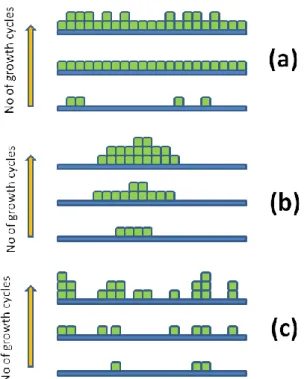
The material arranges itself on the surface in specific manners during ALD growth which is known as the growth mode. Multilayer adsorption should be excluded by definition in ALD growth mode of monolayer per cycle due to self-limiting nature of ALD. In ideal two dimensional layer-by-layer growth mode [Fig. 2.7(a)], material is being deposited in the lowest unfilled material layer as one monolayer of ALD grown material which covers the substrate completely [26,27]. In island growth mode, new units of materials are preferentially deposited on already deposited material by ALD [Fig. 2.7(b)]. Several ALD processes follow this type of growth model [28,29]. Another model named random deposition model is a growth mode in which new material units are deposited on all the surfaces with an equal probability [Fig. 2.7(c)] [30].The growth mode may also change during growth, as for example it may be two dimensional for the initial monolayer and then island or random growth may prevail [31].
Only few of the experimental investigations published so far have found the relationship between growth modes and way in which GPC varies with the number of cycles. It has been found that surface inhibited growth follows the island growth mode [32,33] and linear growth follows two dimensional [34] and random growth mode [35].
11
Figure 1.7: Schematic illustration with increasing number of growth cycles of selected growth modes possible in ALD: (a) two-dimensional growth, (b) island growth, and (c) random deposition.
1.2.6 ALD Window
ALD window is the temperature range in which self-limiting growth occurs. In this temperature range, deposition has an ideal constant growth rate with deposition of one monolayer per cycle. Center line (Fig. 2.8) indicates the ALD window on the growth rate vs. temperature graph. Deviation from ideal self limiting ALD line corresponds to different mechanisms which prevent ALD to attain the requirement of self-limiting reactions. Below the ALD window, there are two possible mechanisms which contribute to non-self terminating reactions. One belongs to high deposition rate due to condensation of precursor molecules on substrate surface at low temperatures. Other belongs to very low deposition rates at low temperatures which is possible due to incomplete reactions due to slower mass transport and low reaction rates. On the other hand, at high temperatures, thermal decomposition occurs which causes a CVD-like growth
12
mechanism in which gas phase decomposition of precursor molecules occurs. In addition, deposition rate may decline at higher temperatures due to desorption of monolayer's deposited by ALD [5].
13
1.2.7 Merits and Demerits of ALD and Comparison with Other
Deposition Techniques
Table 1.2: Merits and demerits of ALD
Merits Demerits
Simple and accurate thickness control by changing the number of reaction cycles
Slow growth rate
Excellent conformality and uniformity Low precursor utilization efficiency
Atomic level control of material composition
High quality material deposition at low processing temperatures No need of reactant flux homogeneity, which enables large area and batch capability
Good reproducibility and straight forward scale-up
No gas phase reactions occur, favoring the usage of precursors that are highly reactive towards each other
Capability to prepare multilayer structures in a continuous process
Table 1.3: Comparison of ALD with other thin film deposition techniques [36].
Method ALD CVD MBE Sputter. Evapor. PLD
Thickness Uniformity Good Good Fair Good Fair Fair
Film Density Good Good Good Good Good Good
Step Coverage Good Varies Poor Poor Poor Poor
Interface Quality Good Varies Good Poor Fair Varies
Low Temp. Deposition Good Varies Good Good Good Good
Deposition Rate Poor Good Fair Good Good Good
Lack of Pinholes Good Good Good Fair Fair Fair
Automated Multilayers Good Fair Good Good Fair Fair
Industrial Applicability Varies Good Varies Good Good Poor
MBE= Molecular beam epitaxy, CVD= Chemical vapour deposition, and PLD- Pulsed laser deposition
14
1.2.8 Classes of Precursors Utilized in ALD
One of the most primary requirements for reactants/precursors that can be utilized in ALD is that they must be volatile and must not thermally decompose in the ALD window (ALD processing temperature where condition of self terminating reaction is satisfied). Other requirements include complete reactions with no etching of the film or the substrate, volatile but inert/non-etching byproducts, and sufficiently high purity. Other common CVD precursor requirements apply as well, such as reasonable cost, easy synthesis and handling, and environmental compatibility [37]. Generally, reactants used in ALD process can be divided in two main categories: inorganic reactants and metal organic reactants.
Metal organic reactants can be further classified in to two sub groups in which one of them contains a direct metal carbon bond and other one contains no direct metal carbon bond. In the group of inorganic reactants most common reactants are halides and elements. While in the group of organometallic reactants, alkyls and cyclopentadienyls are common. Other subclasses of organometallic reactants include alkoxides, diketonates, amides, and amidinates. Elements are the most simple type of reactants used in ALD. They seem very attractive as they carry no extra ligands which can potentially solve the problem of steric hindrance. However, low vapor pressure of elements and their reversible adsorption are the key aspects which limits their usage in ALD processes. Halides are the second class of inorganic precursors which are highly reactive and thermally very stable. In addition to high reactivity, small size of their ligands is very attractive to minimize steric hindrance effect. However, one of the key limitation of halides is their acidic byproducts which are corrosive and can etch the film or reactor components. Alkyls are true organometallic compounds which contain direct metal to carbon bond. These kind of reactants are reactive and their ligands size is also small which helps in reducing the steric hindrance effect. The disadvantage of alkyls is their low decomposition
15
temperature. In this thesis, TEB is used as metal precursor for growth of BN thin film and nanostructures which is an alkyl precursor and contains direct metal to carbon bond. The common non-metal precursors used in ALD processes are: water (H2O), oxygen (O2), ozone (O3), alcohols (R-OH), hydrogen peroxide
(H2O2), atomic oxygen created from plasma as the O2, ammonia (NH3) or
nitrogen/ammonia (N2/NH3) plasma [38,39].
1.2.9 Plasma vs. Thermal ALD
Exchange reactions between precursor molecules and surface species can be enhanced by providing an external source of activation energy. In the conventional mode of ALD, called thermal ALD, activation energy is provided thermally by heating the entire reactor chamber or the substrate. One alternative of thermal ALD is enhanced ALD (PEALD) (also called as plasma-assisted ALD, PA-ALD), in which plasma is utilized to create high energy ions and radicals which enhance the surface reactions by providing an additional source of activation energy.
PEALD open the door for the usage of temperature sensitive substrates in ALD by lowering the deposition temperature. Also, with the use of PEALD, reactants which decompose at higher temperatures can be utilized for surface reactions of ALD. PEALD enables shorter deposition times (higher growth rates), which increase the throughput and make it more attractive for mass production. The main drawback or limitation of PEALD process is reduced conformality on high aspect ratio structures, which is due to the recombination of radicals in deep trenches of high aspect ratio nanostructures.
In comparison with thermal ALD, the PEALD chamber configuration is more complicated. There are three main reactor configurations for PEALD depending on the position of the plasma source, namely, radical-enhanced, direct, and remote plasma systems (Figure 2.9). The first ALD reactor
16
configuration is radical-enhanced ALD which is a modified version of thermal ALD with the addition of a plasma generator [Fig 2.9(a)]. Plasma generation takes place relatively far distance from substrate surface. Therefore, ions and radicals recombine before reaching the substrate. Radicals with low surface recombination probability are needed in this type of configuration in order to increase the efficiency.
In direct plasma configuration [Figure 2.9(b)], a capacitive-coupled plasma is generated at radio frequency (RF, 13.56 MHz) between two parallel electrodes in which one of them is powered while the other one is grounded. Fluxes of plasma radicals and ions are very high in this configuration since plasma is generated very close to substrate surface. As a result, even short exposure times provide uniform deposition on larger wafer surfaces. Processing conditions must be optimized carefully for the sake of avoiding plasma damage from emission of high energy photons.
Remote plasma ALD [Figure 2.9(c)] refers to generation of plasma source at a remote location from substrate holder. The main advantage of this configuration is the high flux of radicals as compared to radical enhanced ALD due to generation of downstream plasma. In addition, this configuration provides better control over plasma and substrate conditions which is not possible for direct plasma ALD.
17
Figure 1.9: Three main types of plasma reactor configurations for PEALD. (a) Radical-enhanced, (b) direct plasma, and (c) remote plasma configurations [40].
The plasma source used in this thesis for deposition of BN thin film and nanostructures is hollow cathode plasma (HCP) source in HCPA-ALD reactor. It has a major advantage over inductively couple and microwave plasma sources
18
in terms of low oxygen contamination. Oxygen contamination is a major problem with inductively couple and microwave plasma sources that arise due to interaction between the plasma species and ceramic introduction windows. Easy scalability and reduced start up times are the other advantages that HCP possess [41].
1.3 Motivation
Being a member of III-nitride family, boron nitride (BN) and its nanostructures have recently attracted a lot of attention, mainly due to their distinctive and superior material properties, including wide band gap, high-temperature stability, high oxidation and corrosion resistance, as well as high thermal conductivity. This versatile material has found applications in UV emission, lubrication, composite reinforcement, gas adsorption, cosmetics, and thermal management. In order to fulfill the entire spectrum of hBN applications, it is imperative to obtain high quality BN films on large area substrates with precise and uniform thickness control. Moreover, a reliable and relatively facile method is necessary to obtain BN films at low temperatures compliant with the standards in terms of having nontoxic byproducts. The need for high-quality and conformal ultra-thin films on large area substrates together with the development of suitable deposition techniques has increased in recent years. These specific requirements, which cannot be fulfilled using conventional physical vapor deposition (PVD) or chemical vapor deposition (CVD) methods, can be met by ALD. In addition, with the combination of ALD and electrospinning, BN nanostructures can be fabricated which might be utilized to address and solve important constraints associated with previous methods of functional nanostructured materials synthesis, such as severe preparation conditions, limited control over morphology, and low purity of the resulting BN nanotubes.
19
Unlike other CVD methods, ALD is based on the saturative surface reactions, which results in a self-limiting growth mechanism. As a result, excellent conformality and large-area uniformity in addition to accurately controlled film thickness are inherently obtained. The processing temperatures can also be kept low, which makes ALD attractive and applicable for a wide range of substrates including transparent and flexible polymers.
1.4 Objectives
This thesis mainly focuses on the growth recipe development and material characterization of BN deposited via sequential injection of triethylboron (TEB) and N2/H2 plasma using a hollow-cathode plasma source integrated ALD
reactor. Nonhalide, alkyl precursors have been utilized for the first time to achieve controlled deposition of BN. In addition, tris–dimethylamino borane (TDMAB) has been used as an alternative precursor for the low-temperature deposition of BN. The main aim of the work is to obtain high-quality, conformal, and uniform deposition of BN films on large area substrates using hollow cathode plasma-assisted ALD (HCPA-ALD) at low substrate temperatures with a systematic optimization of growth parameters such as pulse length of precursors and substrate temperature.
Another goal of this work was to demonstrate the effectiveness of the ALD method to fabricate ceramic nanostructures. To achieve this goal, AlN/BN HNFs were fabricated using a template-based method, which combines the electrospinning, ALD, and CVD processes sequentially. As a proof of concept study, we report on structural, morphological and compositional properties of AlN/BN bishell HNFs fabricated via successive combination of HCPA-ALD and sequential plasma-assisted CVD on electrospun polymeric nanofibrous templates.
20
1.5 Literature overview
1.5.1 BN Thin Film Deposition Using HCPA-ALD Reactor
BN and carbon are isoelectronic and isostructural analogues of each other. Similar to carbon materials, BN can exist in the form of different phases such as amorphous (aBN), turbostratic (tBN), hexagonal (hBN), and cubic (cBN). Among the known two-dimensional materials, hBN and graphene are isostructural, yet their physicochemical properties are different. Graphene is the most prominent member of family of layered materials while hBN is an inorganic analog of graphene. hBN structure consists of layers of hexagonal sheets, which establishes it as an insulator with a direct band gap of ~5.9 eV in its single crystal form [42,44]. Boron and nitrogen atoms are bonded together with a strong covalent bond within each hBN sheet, while different layers of hBN are bound by Van der Waals forces along the c-axis at a distance of 6.66 Å. Different phases of BN have been used as powders and coatings in their pure form or as a composite. This versatile material has found applications in metallization, metal industry, high temperature furnaces, cosmetics, and thermal management. hBN is mainly used for high temperature crucibles and evaporator boats, and as a lubricant due to its layered structure. hBN offers a significant advantage over conventional lubricants due to its high temperature stability and high oxidation resistance [42-49]. The interest in the fabrication of thin films and coatings of either hBN or cBN stems from their high structural strength, high temperature stability, high oxidation resistance, low surface energy, and high thermal conductivity, which already led to numerous technological applications. Application of hBN as a dielectric layer for graphene based electronics has been reported. UV lasing has also been demonstrated with the production of high quality hBN flakes by Kubota et al. Their high quality hBN flakes paved the way to demonstrate applications of hBN in UV light emitting diodes [45,46].
21
Producing high quality BN thin films has proven to be very challenging. BN films deposited by physical vapor deposition (PVD) suffer from poor adhesion and cracking [50,51], whereas BN films deposited by CVD might result in a mixture of hBN, tBN and cBN phases [52,54]. Boron/nitrogen precursors used to obtain hBN films through CVD are reported as BF3/NH3,
BCl3/NH3,and B2H6/NH3 [55-57]. Post-deposition annealing is routinely utilized
for structural enhancement, surface roughness control and intrinsic stress elimination in thin films. Structural ordering of hBN has been accomplished using proper annealing. Researchers have also employed ALD technique for BN thin film deposition to obtain highly conformal and uniform BN films with simple thickness control. BN films obtained via ALD were either aBN or tBN, in which BBr3/NH3 and BCl3/NH3 were utilized as boron/nitrogen precursors,
respectively [58-60]. Substrate temperatures for self-limiting growth was reported to be in the range of 250-750 C. However, due to the nature of these halide precursors, the byproducts of surface reactions are hazardous and corrosive [61,62]. hBN deposition with borazine, which is a non-halide precursor, has been reported to result in a monolayer limited deposition under ultra high vacuum conditions on transition metal surfaces [63,64]. The deposition terminated or became very slow after the formation of an initial monolayer of BN, therefore deposition was believed to be surface inhibited due to the inert nature of boron nitride.
1.5.2 Fabrication of Aluminium Nitride (AlN)/BN Bishell
Hollow Nanofibers (HNFs)
AlN and BN have similar lattice parameters and they are well known for their attractive properties, mainly including large band gap, high temperature stability, high oxidation and corrosion resistance, and high thermal conductivity. Nanostructures of AlN have emerged as a promising candidate for high surface area, highly sensitive biological and chemical sensors [65,66]. Mostly AlN
22
tubular structures have been synthesized at high temperature using template free methods. Recently our group has reported template based synthesis of AlN at temperatures as low as 200C using electrospinning and ALD [67].
BN and boron nitride nanotubes (BNNTs) are structural analogues of carbon and carbon nanotubes (CNTs) respectively. BN exists in the various forms such as rhombohedral (r-BN), hexagonal (h-BN), cubic (c-BN), turbostratic (t-BN) and amorphous (a-BN) [68]. In contrast to metallic or semiconducting CNTs, BNNT has band gap of 5.5 eV, independent of tube chirality and morphology. Primarily, the interest in BN nanotubes arose due to a recognized fact that layered BN structure is much more thermally and chemically stable then graphite carbon structure. Later on, researchers have demonstrated that BNNTs exhibit far better thermal and chemical stabilities than CNNTs. With these inherited properties in BN tubular structures, researchers have shown BNNTs application in composite reinforcement, gas adsorption, membrane filters,field emitters, and ultraviolet light emitters [69].
In the recent years fibrous hollow structures have gathered huge interest of researchers due to their unique characteristics such as large surface area, high aspect ratio, and open pore structures. The pioneering work in BNNTs synthesis was conducted by Chopra et al. [70],followed by some other groups [71,72]who prepared BNNTs by arc discharge method. However carbon impurities were present in those tubes and BN nanoparticles were yielded with BNNTs and observed at BNNTs tip ends. Laser ablation synthesis of BNNTs was reported by Golberg et al. [73], where a continuous CO2 laser was focused on BN targets
at higher temperatures. Limitations associated with this method is the high percentage of BN flakes that were obtained with a rather small number of BNNTs. CVD synthesis of BNNTs have been reported by Lourie et al. [74], at higher temperatures ranging from 700-1100 C. However, In contrast with hundred of grams CVD yielded CNTs, Researchers have struggled to obtain huge amount of BNNTs with CVD. Instead a milligram product has been obtained containing BNNTs. In this thesis, we report on AlN/BN bishell HNFs fabrication by a combination of electrospinning and HCPA-ALD.
23
Chapter 2
Experimental Details
This chapter provides a detailed explanation of boron nitride (BN) thin film deposition and fabrication of aluminium nitride (AlN)/BN bishell hollow nanofibers (HNFs) as well as the materials characterization techniques. All of the deposition and fabrication processes were performed at UNAM Cleanroom Facility (UCF) and UNAM characterization tools were used for materials property evaluation of thin film and nanostructured BN materials.
2.1 BN Deposition Using Sequential Injection of
Triethylboron (TEB) and N
2/H
2Plasma
BN thin films were deposited on silicon (Si) (100) wafers. Substrate cleaning procedure started with 5 min sequential ultrasonic agitation in isopropanol, acetone, methanol, and de-ionized (DI) water. Following that, substrates were immersed in (1:25) HF: H2O mixture for 1 min to remove native oxide on
substrate surface. At the end of cleaning procedure, Si (100) wafer pieces were rinsed with DI water and dried using nitrogen (N2) gun.
24
Depositions were performed in a modified Fiji F200-LL atomic layer deposition (ALD) reactor (Cambridge Nanotech Inc., Cambridge, MA) which is equipped with a stainless steel hollow cathode plasma source (Meaglow Ltd., Thunder Bay, ON, Canada). The Fiji is a modular high-vacuum ALD system which is capable of carrying out thermal as well as plasma-enhanced depositions. The details of the system are presented in Fig. 3.1.
Figure 2.1: Details regarding specific parts and their features of ALD system
BN thin films were deposited on pre-cleaned substrates using sequential exposures of TEB and N2/H2 plasma at temperatures ranging from 250 to 450
C. Due to its relatively low vapor pressure (boiling point = 95 C), TEB precursor was heated up to 45 C. The base pressure of the system was kept at 150 mTorr. TEB and N2/H2 were carried from separate lines using 30 and 100
sccm Ar, respectively. N2/H2 gas flow rates and plasma power were kept
constant in all experiment as 50/50 sccm and 300 W, respectively. Ar was used as a purging gas with 10 and 20 s of purge duration.
25
2.2 BN Deposition using Sequential Injection of
Tris(dimethyl)amidoboron (TDMAB) and N
2/H
2Plasma
BN thin films were deposited on silicon (Si) (100) wafers. Substrate cleaning procedure started with 5 min sequential ultrasonic agitation in isopropanol, acetone, methanol, and de-ionized (DI) water. Following that, substrates were immersed in (1:25) HF: H2O mixture for 1 min to remove native oxide on
substrate surface. At the end of cleaning procedure, Si (100) wafer pieces were rinsed with DI water and dried using nitrogen (N2) gun.
Depositions were performed in a modified Fiji F200-LL ALD reactor (Cambridge Nanotech Inc., Cambridge, MA) which is equipped with a stainless steel hollow cathode plasma source (Meaglow Ltd., Thunder Bay, ON, Canada). The details of the system are given in Fig. 3.1. BN thin films were deposited on pre-cleaned substrates using sequential exposures of TDMAB and N2/H2 plasma
at temperatures ranging from 50 to 400 C. 800 growth cycles were carried out and one hollow cathode plasma-assisted ALD (HCPA-ALD) cycle consisted of 0.06 s TDMAB pulse/10 s Ar purge/40 s N2/H2 plasma (50/50 sccm, 300 W)/10
s Ar purge.
2.3 Post-growth Annealing of BN Thin Films
BN deposited on Si substrate by exposures of TEB and N2/H2 plasma was
annealed at 800 C for 30 min, while BN deposited on Si substrate by exposures of TDMAB and N2/H2 plasma was annealed in the temperature range of 300-900
C for 30 min in N2 atmosphere using ATV–Unitherm (RTA SRO-704) rapid
thermal annealing system. Effect of post-growth annealing on structural, optical, morphological and chemical properties was studied using these samples.
26
2.4 Fabrication of AlN/BN Bishell HNFs by
Combination of Electrospinning and ALD
A four-step fabrication process was utilized to fabricate the AlN/BN HNFs. 1) In the first step, nylon 6,6 templates was prepared by electrospinning. 2) AlN growth was carried out on electrospun polymeric nanofibrous template
using alternating exposures of trimethyl aluminium (TMA) and N2/H2
plasma as aluminium and nitrogen precursors, respectively.
3) AlN HNFs have been obtained by removing the core polymeric template by calcination.
4) As a last step, BN has been deposited on AlN HNFs using TEB and N2/H2
plasma as alternating precursors for boron and nitrogen to obtain AlN/BN bishell HNFs.
2.4.1 Electrospinning of Nylon Nanofibrous Sacrificial
Templates
Nylon 6,6 having 8 wt.% (w/v) was dissolved in formic acid by stirring for 3 h at room temperature, for each sample. The resulting homogeneous clear solution was placed in 10 ml syringes fitted with metallic needles having inner diameter of 0.8 mm. The syringes were fixed horizontally on the syringe pump (Model: SP 101IZ, WPI). The polymer solution was pumped with feed rate of 1 mL/h during electrospinning and the tip-to-collector distance was set to 10 cm. 15 kV was applied to the metal needle tip using high voltage power supply (Matsusada, AU Series) for the electrospinning of the polymer solution. The solvent evaporated on the way to the grounded stationary cylindrical metal collector (height: 15 cm, diameter: 9 cm) covered with a piece of aluminium foil. The randomly oriented electrospun nylon nanofibers were deposited onto Si wafer which was fixed on the aluminium foil. The electrospinning setup was enclosed
27
in a Plexiglas box and the electrospinning was carried out at 23 °C and 36% relative humidity.
2.4.2 Atomic Layer Deposition of AlN
200 cycle ALD growth of AlN was carried out on electrospun nanofibers at 100 °C in a Fiji F200-LL ALD reactor (Cambridge Nanotech Inc., Cambridge, MA), which is equipped with a stainless steel hollow cathode plasma source (Meaglow Ltd.), with a base pressure of 150 mTorr. Precursors utilized for the growth of AlN were TMA and N2/H2 plasma with argon (Ar) as the carrier and
purge gas. One hollow cathode plasma assisted ALD (HCPA-ALD) cycle consisted of 0.06 s TMA pulse/10 s Ar purge/40 s N2/H2 plasma (50/50 sccm,
300 W)/10 s Ar purge.
2.4.3 Removal of Sacrificial Nanofibrous Polymeric Templates
AlN growth was followed by the calcination of AlN-coated nylon nanofibers in air ambient at 500 °C for 2 h in order to remove the polymeric core. Nylon polymer template decomposition procedure is based on high temperature calcination technique.
2.4.4 Low-Temperature Sequential CVD of BN
Following the calcination/ethanol treatment of AlN-coated polymeric nanofibers, AlN HNFs were introduced into the same ALD reactor and coated with BN at 450 °C to obtain AlN/BN bishell HNFs. 1000 growth cycles of BN was carried out utilizing TEB and N2/H2 plasma sequentially as boron and
nitrogen precursors with Ar as carrier and purge gas. One growth cycle consisted of 0.12 s TEB pulse/20 s Ar purge/40 s N2/H2 plasma (50/50 sccm,
28
100 sccm, respectively. Samples were taken out from the reactor through a load-lock and exposed to air as soon as the ALD reactor cooled down to 200 °C.
2.5 Characterization Methods
In SEM, specimen is bombarded by a focused beam of high energy electrons which is rastered across the surface of the specimen. This electron beam generates a variety of signals (secondary electrons, back scattered electrons, and characteristic X- rays), which are emitted from the area of specimen exposed to electron beam [75]. These signals provide valuable information about topography and composition of the sample. In this study, Nova NanoSEM (FEI) was used to reveal surface morphology, uniformity, and HNFs dimensions of the nanostructured samples. Prior to imaging, BN thin film and AlN/BN nanostructures were coated with 5 nm Au/Pd to eliminate the charging effect.
AFM is a high resolution scanning probe microscopy (SPM) that may be used to obtain micro- and nano-scale morphology of a wide range of samples, including both conductive and insulating materials [76]. In this study, surface morphologies of the BN thin films were revealed using an atomic force microscope (AFM) (XE-100E, PSIA, Suwon, Korea), operated in the contact mode.
XPS is a widely used technique to determine quantitative atomic composition of solid surface. Moreover, this technique provides other significant thin film material information such as elemental composition, chemical bonding state information, and uniformity of sample surface without the restriction on type of material being analyzed [77, 78]. In this work, elemental composition and chemical bonding states of the BN films and AlN/BN nanostructures were determined by XPS using Thermo Scientific K-Alpha spectrometer (Thermo Fisher Scientific, Waltham, MA) with a monochromatized Al Kα X-ray source. Sputter depth profiling was performed with a beam of Ar ions having an acceleration voltage and spot diameter-size of 1 kV and 400 µm, respectively.
29
X-ray crystallography is a technique, mainly used for identifying phases, atomic and molecular structure, unit cell lattice parameters, average crystallite size of nanocrystalline samples, and crystalline microstrain of a crystalline material [79-81]. In order to obtain information from very thin layers, grazing-incidence XRD (GIXRD) is preferred. In GIXRD, measurements are taken at very small incidence angles (typically smaller than 0.5°), which enables the small penetration depths and intensity enhancement at the surface. Incident angle, the beam path length, and the irradiated area are kept constant and only the detector rotates through the angular range during the collection of diffraction pattern. As a result, GIXRD can be utilized to analyze crystal structures ranging from a few to hundred nanometers below the surface of the solids. In this study, GIXRD patterns were recorded in an X'Pert PRO MRD diffractometer (PANalytical B.V., Almelo, Netherlands) using Cu Kα radiation. Data were obtained within the 2Theta range of 20-80° by the summation of ten scans, which were performed using 0.1° step size and 10 s counting time. Interplanar spacing (dhkl) value for the (010) plane was calculated from peak position using the well-known Bragg’s law. Lattice parameter a was roughly calculated by substituting d010 value in Eqn. 3.1, which relates the interplanar spacing (dhkl),
miller indices (hkl) and lattice parameters (a and c) for hexagonal crystals. (3.1)
By neglecting instrumental broadening and assuming that the observed broadening is only related to the size effect, crystallite size values for the as-deposited and annealed films were estimated from the (010) reflection using Eqn. 3.2, the well-known Scherrer formula
(3.2) where , B and are the wavelength of the radiation used (Cu K = 1.5418 Å),
broadening (FWHM), and Bragg diffraction angle of the selected reflection, respectively.
30
Similar to SEM, TEM also utilizes an electron beam as imaging source. The major difference between SEM and TEM is that, TEM utilizes the transmitted electrons as an imaging source, while SEM detects the reflected electron from specimen surface. SEM focuses on samples surface only while TEM provides the details about internal structure, crystallization, and internal composition [82]. In this study, Tecnai G2 F30 TEM (FEI, Hillsboro, OR) was utilized for the high-resolution (HR) imaging of the BN thin film sample, which was capped with a 20 nm AlN layer prior to TEM sample preparation. AlN was deposited at 200 C using HCPA-ALD. TEM sample was prepared by a Nova 600i Nanolab focused ion beam (FIB) system (FEI, Hillsboro, OR) at an acceleration voltage of 30 kV using various beam currents ranging from 50 pA to 21 nA. Damage layer was removed by FIB milling at a beam voltage of 5 kV. Elemental mapping was performed in TEM, using an energy dispersive X-ray spectrometer (EDXs). TEM, energy dispersive X-ray spectroscopy (EDXs), and selected area electron diffraction (SAED) analyses of AlN/BN nanostructures were performed using same TEM. TEM samples for AlN/BN nanostructures analysis were prepared by scratching hollow nanofibers from the substrate and dispersing them into ethanol, followed by sonification and drop casting onto copper grids.
Ellipsometry measures the change in polarization state of light reflected from the surface of the sample. The most common applications of ellipsometer include the measurement of film thickness and optical constants (refractive index and extinction coefficient) in UV, visible, and IR range. In this study, optical constants of the BN films were determined using a variable angle spectroscopic ellipsometer (V-VASE, J.A. Woollam Co. Inc., Lincoln, NE) which is equipped with rotating analyzer and xenon light source. The ellipsometric spectra were collected at three angles of incidence (65o, 70o, and 75o) to yield adequate sensitivity over the full spectral range. Optical constants and film thicknesses were extracted by fitting the spectroscopic ellipsometry data. The numerical iteration was performed to minimize the mean-square error function using WVASE32 software (J.A. Woollam Co. Inc., Lincoln, NE). The
31
homogeneous Tauc-Lorentz (TL) function was used as an oscillator. In addition, data fitting was improved using the Bruggeman effective medium approximation at the film-air interface assuming 50% film and 50% voids. The absorption coefficient, , was calculated from the k values determined from the ellipsometry data. Optical band gap (Eg) is expressed by the Eqn. 3.3 for direct band gap materials [83], which can be analytically extracted via extrapolation of the linear part of the absorption spectrum to
(3.3)
Ultraviolet-visible (UV-VIS) spectrophotometry is used to measure the absorption or transmission spectra in the UV-VIS spectral region. Incident photon energy is absorbed by the electrons which can be excited to higher orbital's (such as π-electrons). In this study, spectral transmission measurements were performed with a UV-VIS spectrophotometer (HR4000CG-UV-NIR, Ocean Optics Inc., Dunedin, FL) in the wavelength range of 220-1000 nm relative to air.
32
Chapter 3
Results and Discussions
This chapter presents the experimental results of boron nitride (BN) thin film, growth recipe optimization, aluminium nitride (AlN)/BN hollow nanofibers (HNFs) fabrication process regarding electrospinning of polymeric templates, hollow cathode plasma-assisted atomic layer deposition (HCPA-ALD) of AlN, and sequential chemical vapor deposition (CVD) of BN. Moreover, optical, morphological, structural, and compositional characterization results of BN thin films and AlN/BN HNFs are also discussed in detail.
3.1 BN Thin Films Growth Using Sequential
Exposure of Triethylboron (TEB) and N
2/H
2Plasma
Deposition experiments of BN were carried out within the temperature range of 250-450 C by the sequential injection of TEB and N2/H2 plasma. TEB belongs
to alkyl (organometallic) class of precursors. Alkyls are known as true organometallic compounds as they contain direct metal-to-carbon bond, which
33
makes them very reactive. The primary and foremost reason for selecting TEB as boron precursor was its non-halide nature. As alkyl precursors don't possess halide metal bonds, their gaseous byproducts with hydrogen containing non metal reactants (N2/H2, NH3) are typically saturated hydrocarbons which don't
reabsorb and are generally inert. Also, steric hindrance effect in alkyl precursor is significantly less as compared to other classes of reactants as they don't have bulky ligands which contribute to steric hindrance [84,85]. This aspect of the alkyl precursors make them quite attractive for ALD processes as films deposited with alkyl precursors generally result in higher GPC with lower impurity contamination [86,87].
3.1.1 Optimization of Growth Parameters
In order to optimize growth parameters for deposition of BN thin films, pulse length of TEB, substrate temperature, Ar purge time, as well as the influence of post-deposition annealing are investigated. One growth cycle consisted of TEB pulse/20 s Ar purge/40 s, 50/50 sccm N2/H2 plasma (300 W)/20 s Ar purge.
Flow rates of N2/H2 plasma, plasma power, and Ar purge length were kept
constant for all the experiments. Hollow cathode plasma source was installed in our ALD system, capable of producing a maximum plasma power of 300 W. It was kept at its maximum power level throughout the experiments to make the N2/H2 radicals highly reactive towards TEB. Initially, same recipe was followed
with 10 s of Ar purge length. Growth per cycle (GPC) was same for both the purge times. However, non uniform surface of substrate with small particles was observed for 10 s of Ar purge which was an indication that 10 s of purging was not enough to completely evacuate the reactor from unreacted excess precursor molecules and gaseous reaction by-products. This problem was solved by increasing the purge length to 20 s of Ar purge.
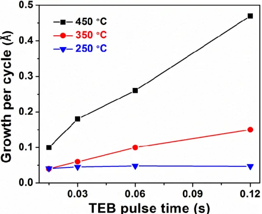
Dependency of GPC of BN on TEB pulse length at different temperatures is given in Fig. 3.1. At 250 C GPC was 0.05 Å and it didn't change with
![Table 1.1: Alternative names of ALD[5]](https://thumb-eu.123doks.com/thumbv2/9libnet/5771124.117031/15.892.300.658.772.1127/table-alternative-names-of-ald.webp)


![Table 1.3: Comparison of ALD with other thin film deposition techniques [36].](https://thumb-eu.123doks.com/thumbv2/9libnet/5771124.117031/26.892.176.783.355.887/table-comparison-ald-film-deposition-techniques.webp)
![Figure 1.9: Three main types of plasma reactor configurations for PEALD. (a) Radical- Radical-enhanced, (b) direct plasma, and (c) remote plasma configurations [40]](https://thumb-eu.123doks.com/thumbv2/9libnet/5771124.117031/30.892.292.649.199.995/figure-plasma-reactor-configurations-radical-radical-enhanced-configurations.webp)