Functionalization of silicon nanowires with transition metal atoms
E. Durgun,1N. Akman,2,3and S. Ciraci1,3,*
1Department of Physics, Bilkent University, Ankara 06800, Turkey 2Department of Physics, Mersin University, Mersin 33343, Turkey
3UNAM-Institute of Materials Science and Nanotechnology, Bilkent University, Ankara 06800, Turkey
共Received 7 May 2008; revised manuscript received 23 September 2008; published 18 November 2008兲
This paper investigates atomic structure, mechanical, electronic, and magnetic properties of silicon nano-wires共SiNW兲 using first-principles plane-wave calculations within density-functional theory. We considered bare, hydrogen-terminated, and 3d-transition metal共TM兲 adsorbed SiNWs oriented along 关001兴 direction. We also studied Cr interstitial impurity. Nanowires of different sizes are initially cut from the bulk Si crystal in rodlike forms, and subsequently their atomic structures are relaxed before and also after the termination of surface dangling bonds by hydrogen atoms. We first presented an extensive analysis of the atomic structure, stability, elastic, and electronic properties of bare and hydrogen-terminated SiNWs. The energetics of adsorp-tion and resulting electronic and magnetic properties are examined for different levels of 3d-TM atom cover-age. Adsorption of TM atoms generally results in magnetic ground state. The net magnetic moment increases with increasing coverage. While specific SiNWs acquire half-metallic behavior at low coverage, at high coverage ferromagnetic nanowires become metallic for both spin directions, and some of them have very high spin polarization at the Fermi level. Our results suggest that the electronic and spintronic devices with con-ducting interconnects between them can be fabricated on a single SiNW at a desired order. We believe that our study will initiate new research on spintronic applications of SiNWs.
DOI:10.1103/PhysRevB.78.195116 PACS number共s兲: 72.25.⫺b, 73.63.Nm, 75.75.⫹a
I. INTRODUCTION
One of the major obstacles in miniaturization of solid-state electronic devices has been the fabrication of intercon-nects having diameters compatible with the size of devices they connect. Not only in solid-state electronics but also in nanoelectronics, interconnecting nanodevices or molecular devices has remained a challenge for several decades. An active research was carried out during the last decade on the mechanical, electronic, and transport properties of one-dimensional 共1D兲 nanowires, including monoatomic chains, wires having a few atoms in their cross section,1,2 and nanotubes.3 Initially, suspended monoatomic chains of gold has been a breakthrough in the field.4Presently, the practical applications of monoatomic chains appear to be unrealistic even if their stability and quantum transport properties have been understood to a great extent. Recently carbon nanotubes have been the focus of attention owing to their nanoscale diameter and regular cylindrical shape. Furthermore, the outer surface of these tubes can be coated uniformly by Ti atoms allowing high conductance.5,6 Despite these advan-tages, the use of carbon nanotubes as an interconnect are hindered because of difficulties in controlling their diameter during the synthesis.
While the search for feasible interconnects in nanoelec-tronics are continuing, nanosized Si nanowires共SiNW兲 have appeared to be an attractive 1D material because of the well-known silicon-based microelectronic fabrication technology and their use directly on the Si-based chips. SiNWs display diversity of electronic properties depending on the number of Si atoms in their cross section. The linear monatomic Si chain is metallic with quantum ballistic conductance three times higher than that of gold.7The linear Si chain is, how-ever, metastable and hence it changes to a metallic zigzag
chain.7Stable nanowires made of Si pentagons perpendicular to the wire axis have been reported.8Based on the prediction of first-principles calculations, Si can also form tubular struc-tures made of hexagons similar to that of carbon nanotubes. Depending on the chirality and diameter, these tubular struc-tures can exhibit metallic or semiconducting behaviors.9
Silicon nanowires have been produced using various ex-perimental methods.10–14 The formation of an oxide layer around SiNW with a minimum thickness of 1–3 nm appears to be a disadvantage.15 Nevertheless, rodlike SiNWs with a diameter of 1.3–7 nm have been prepared more recently. Their oxide layer can be removed from their surface and the dangling bonds at the surfaces can be terminated with hydrogen.16The experimental findings have indicated a crys-talline core surrounded by an outer surface for the atomic structure of the SiNWs. Whether this crystalline core is tet-rahedral 共diamondlike as in bulk Si兲 or is of any other ar-rangement of atoms has been the subject of further investi-gation. Fullerene-like 共cagelike兲 nanowires have been proposed and investigated theoretically in Refs. 17and 18. Diamondlike and cagelike wires are compared energetically in Ref.18. Besides, single crystalline and polycrystalline na-tures of very thin silicon nanowires have been theoretically investigated by Zhao and Yakobson.19
The thinnest SiNW 共having radius R⬃0.65–3.5 nm兲 synthesized so far has been grown along the 关110兴 and the 关112兴 directions.16 SiNWs with sizes less than 10 nm have been also reported along different directions such as关001兴,20 关110兴,20,21 关111兴,21 and关112兴.21 Theoretically关001兴 oriented SiNW is the most studied wire in the literature. Rurali and Lorente22 studied nonpassivated and undoped 关001兴 SiNWs consisting of 57, 114, and 171 atoms by using density-functional theory共DFT兲. They obtained energetically equiva-lent metallic and semimetallic reconstructions. Tight-binding density-functional calculations on hydrogen-passivated
SiNWs 共Ref.23兲 have presented that, while 关112兴 wires are
the most stable ones, 关001兴 wires have the widest energy-band gap. By passivating the SiNW surface with some halo-gens including Br, Cl, and I, the electronic structure of dif-ferent sized wires ranging from 0.6 to 3 nm have been studied using ab initio density-functional theory calculations.24
Experimental and theoretical studies so far have shown that those SiNWs exhibit a wide range of physical and chemical properties, which may be of interest in technologi-cal applications.25,26 Depending on whether the dangling bonds on their outer surface are saturated with hydrogen at-oms and the shape of their cross section, they exhibit semi-conducting or metallic behavior. Usually, unsaturated dan-gling bonds on the outer surface attribute a metallic character to a SiNW. Upon saturation of these dangling bonds, a SiNW becomes a semiconductor. Moreover, the band gap of semi-conductor SiNWs vary with their diameter. Not only the band gap but also the stability of a SiNW strongly depends on its diameter.
Silicon nanowires can function in various electronic and optical applications such as field effect transistors27共FETs兲, light emitting diodes,28 lasers,29 and interconnects. Its con-ductance can be tuned by doping during the production pro-cess or by applying a gate voltage in a SiNW FET. In various device applications, such as diodes and transistors, n- and
p-doped SiNWs 共Refs. 25, 30, and 31兲 have also attracted
interest. Furthermore a growing research interest has been devoted to the functionalization of SiNW surface with vari-ous species to study the chemical and biological sensitivities of silicon nanowires.32–34 H-saturated SiNW and GeNW, which have band gaps of different widths, can form pseudo-morphic heterostructures.35It has been predicted that the pe-riodic, H-saturated SiNW共N兲/GeNW共N兲 heterostructure su-perlattices behave as a multiple quantum well structure with confined states.35
This paper presents an extensive study on the mechanical, electronic, and magnetic properties of bare, H-passivated SiNWs oriented along the 关001兴 direction, as well as those functionalized by 3d-transition metals 共TMs兲. Preliminary results of this study were published as a short letter.36 Our study is based on the first-principles plane-wave calculations using DFT and ab initio molecular-dynamics 共MD兲 calcula-tions using microcanonical ensemble. The organization of the paper is as follows: in Sec. II, we summarize essential aspects of the method and its relevant parameters used in the calculations. In Sec. III we present a systematic and brief summary of our results on the atomic structure, reconstruc-tion, energetics, mechanical, and electronic properties of bare and hydrogen-terminated SiNWs of different cross sections. Section IV deals with the functionalization of SiNWs with light TMs, such as Ti, Fe, Co, Cr, and Mn. First, adsorption geometry and energetics are examined for the adsorption of a single TM atom 共per primitive cell designated as ⌰=1兲 on the surface of SiNWs. It was found that TM-doped H-saturated SiNWs have ferromagnetic ground state and some of them exhibit half-metallic 共HM兲 behavior with 100% spin polarization at the Fermi level 共EF兲.37,38 Upon
increased coverage of TM atoms 共corresponding to ⌰=n, with n being the number of TM atoms adsorbed per primitive
cell兲 of H-saturated SiNWs, the HM character is disturbed but spin polarization continues to be very high for specific nanowires. High magnetic moment and also high spin polar-ization for certain cases achieved at high⌰ can be important for applications in biotechnology and spintronics. Our results are of fundamental and technological interests since room-temperature ferromagnetism is already discovered in Mn+-doped SiNW.39 The paper is concluded with our con-clusions in Sec. V.
II. METHOD
We have performed first-principles plane-wave calculations40–42 within DFT.43All calculations for nonmag-netic, ferromagnonmag-netic, and antiferromagnetic states are carried out using ultrasoft pseudopotentials.41,44The results of these calculations were also confirmed by calculations using pro-jector augmented wave 共PAW兲 potential.45 The exchange-correlation potential has been approximated by generalized gradient approximation 共GGA兲 共Ref. 46兲 both for
spin-polarized and spin-unspin-polarized cases. For partial occupancies we used the Methfessel-Paxton smearing method.47All struc-tures have been treated within supercell geometry using the periodic boundary conditions with cell dimensions of a and b ranging from 20 to 30 Å, depending on the diameter of the SiNW, in order to provide 10 Å vacuum space, and along the wire axis c = c0 共c0 being the relaxed lattice constant of SiNW兲. In the self-consistent potential and total-energy cal-culations, the Brillouin zone共BZ兲 of supercell is sampled in the k space within Monkhorst-Pack scheme48 by 共1⫻1 ⫻15兲 mesh points. A plane-wave basis set with maximum kinetic energy of 350 eV has been used.
For the calculation of magnetic moments, the charge den-sity of spin-up and spin-down electrons is calculated sepa-rately. Spin-polarized total energy ETsp is calculated by start-ing with different initial magnetic-moment 共兲 values and subsequently by relaxing them together with the atomic structure. This way, the trapping of the magnetic moment in a local minimum has been avoided. To check whether anti-ferromagnetic ground state of H-saturated SiNW共N兲+TM exists, spin-polarized calculations have been carried out in supercell including double primitive cell of the nanowire, where adjacent TM atoms may have opposite spins.
All atomic positions and lattice constants are optimized by using the conjugate gradient method where total energy and atomic forces are minimized. The convergence for en-ergy is chosen as 10−6 eV between two ionic steps, and the maximum force allowed on each atom is 10−3 eV/Å. To relieve the constraints imposed by periodic boundary condi-tions, the calculations related with the study of reconstruc-tion have been repeated using supercells with c = 2c0and 4c0 共namely, comprising double and quadruple unit cells of SiNW, respectively兲.
III. PROPERTIES OF BARE AND HYDROGEN-PASSIVATED SILICON NANOWIRES
In this paper, we consider the rodlike bare and H-terminated Si nanowires oriented along 关001兴 direction
having different diameters 共or different number of Si atoms in their unit cell兲. The bare Si nanowire oriented along 关001兴 direction and having N Si atoms in the primitive unit cell is specified by SiNW共N兲. Similarly, a nanowire with all dan-gling bonds on the surface passivated by H atoms after re-laxation is specified by H-SiNW共N兲. If the dangling bonds are saturated before relaxation it is specified as H-SiNW共N兲-b. The sequence of structure optimization is crucial for the electronic properties. Here, the structure opti-mization of H-SiNWs is achieved in two steps. Initially, SiNWs are cut in rodlike forms from the bulk Si crystal共see Fig. 1兲. Subsequently, the initial atomic structure having
ideal bulk configuration is relaxed to yield the minimum total energy with the atomic forces smaller than 10−3 eV/Å 共see upper panels of Fig.2兲. In the second step, hydrogen
passi-vation of bare SiNWs is achieved by termination of the dan-gling bonds of Si atoms共which have nearest-neighbor
coor-dination less than four Si atoms兲 by H atoms. Subsequently, whole structure that includes H atoms is optimized again共see lower panels of Fig. 2兲. An alternative way of structure
op-timization was also carried out in several theoretical studies in single step: first, the dangling bonds on the surface of the ideal bare SiNW cut from the bulk crystal are saturated by H atoms and subsequently whole structure has been optimized once. The latter optimization process, however, leads to elec-tronic structure different from the former two-step process done in the present study. It should be noted that the two-step process better mimics the actual growth process. The results for single-step relaxation, i.e., H-SiNW共N兲-b, are also in-cluded for comparison. This section presents a comparative study of atomic structure, reconstruction, electronic band structure, and elastic properties of structure-optimized bare and H-passivated SiNWs. Thereafter, it will be clear that the properties of optimized bare SiNWs are quite different from those of H-SiNWs.
A. Atomic structure and energetics
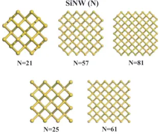
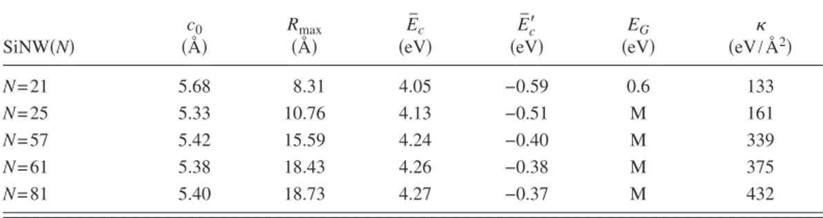
Figure 2 shows the atomic structures of optimized bare SiNWs and H-SiNWs investigated in this paper. We consid-ered wire geometries having 21, 25, 57, 61, and 81 Si atoms in the primitive unit cell. Among these wires, nanowires 21, 57, and 81 have rather round cross sections while those of 25 and 61 have squarelike cross sections.
The cohesive energy共per Si atom兲 of the bare SiNWs is calculated by E¯c= ET关Si兴−ET关SiNW共N兲兴/N, in terms of the
total energy of free Si atom and the total energy of bare SiNW共N兲 having optimized structure. According to this defi-nition, E¯c⬎0 indicates that the structure is stable with
re-spect to constituent free atoms. The cohesive energy relative to the bulk Si crystal, E¯c
⬘
= ET关Bulk Si兴−ET关SiNW共N兲兴/N, iscalculated by replacing the free-atom energy with the total energy of bulk equilibrium crystal per Si atom, i.e.,
ET关Bulk Si兴. The binding energy of hydrogen with respect to
the free H atom is also of interest and is calculated by Eb
=共NHET关H兴+ET关SiNW共N兲兴−ET关H-SiNW兴兲/NH, in terms of
the total energy of structure-optimized bare SiNW共N兲 and H-SiNW共N兲 terminated by NHhydrogen atom and the energy of free H atom, ET关H兴. The binding energy of hydrogen
rela-tive to H2molecule, Eb
⬘
, is obtained if ET关H兴 is replaced byET关H2兴/2. Calculated structure parameters, such as the lattice
constant along the wire axis c0, maximum radius of the cross section, cohesive energy relative to free Si atom and Si crys-tal, and binding energy of H atom, are presented in Tables I
andII.
In general, the lattice constant c0 of optimized bare and H-SiNW共N兲 decreases with increasing N. Namely, the lattice constant is large for small N but approaches the lattice con-stant of bulk Si. This trend is, however, different for N = 25 and 61, which form a class of nanowires with squarelike cross sections.
E ¯
cis comparable with the cohesive energy of bulk crystal
calculated to be 4.46 eV/atom, and expectantly it increases with increasing N. As for the average cohesive energy rela-tive to the bulk Si crystal E¯c
⬘
, it is small but negative as SiNW (N) N=21 N=25 N=57 N=61 N=81FIG. 1. 共Color online兲 Atomic structure of the cross section of rodlike Si nanowires as cut from the ideal bulk silicon 关i.e., ideal SiNW共N兲兴 for N=21, 25, 57, 61, and 81.
N=21 N=25 N=57 N=61 N=81
SiNW
(N)
H-SiNW
(N)
FIG. 2. 共Color online兲 Upper panels: Top and side views of optimized atomic structures of bare SiNW共N兲s 共with N=21, 25, 57, 61, and 81兲 cut from the bulk Si crystal along 关001兴 direction. Lower panels: H-SiNW共N兲s which are optimized upon H termina-tion of SiNW共N兲s in the upper panel. Large and small balls indicate Si and H atoms, respectively. Side views consist of two primitive unit cells.
expected. However, its magnitude becomes smaller as N in-creases共namely as the bulk properties start to dominate with increasing diameter兲. The binding of H atom is exothermic with positive binding energy both for Eband also for Eb
⬘
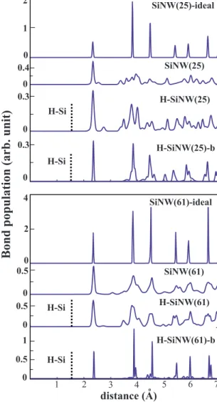
.Atomic structure of SiNWs was analyzed by comparing the distribution of interatomic distances between various at-oms共up to sixth nearest neighbor兲 with that of ideal crystal. In Fig.3, the distribution of interatomic distances are plotted for bare SiNW共N兲, H-SiNW共N兲, as well as H-SiNW共N兲-b for N = 21, 57, and 81. Similar analysis is illustrated in Fig.4
for N = 25 and 61, which have rather square cross sections. The deviations from ideal case are large for small N. The distribution of the first nearest-neighbor distance is always sharp for all N. Significant deviations from the second-, third-, etc. nearest-neighbor distances of ideal bulk crystal are observed. In particular, already the peak related to the distribution of second-nearest-neighbor distance starts to broaden. The structure of optimized bare SiNWs is healed by H termination of dangling bonds. This is seen by the fact that the distribution of distant nearest neighbors appears as peaks coinciding with the ideal structure. Additional peaks are re-lated with surface reconstruction. Clearly, the distribution of H-SiNW共N兲-b is very similar to that of ideal SiNW since the surface relaxation is hindered by saturating the dangling bonds of ideal SiNW.
B. Reconstruction and stability
The surface reconstruction of bare SiNWs is crucial with the resulting electronic properties and hence has been widely
discussed.19,49–51 To ensure that the structures discussed in Fig.2are minimum-energy structure, we performed structure optimization by doubling and also by quadrupling the unit-cell size, where the lattice constant of the superunit-cell is taken to be c = 2c0 and 4c0, respectively. As initial structures, we took always the structure of ideal SiNW as cut from the ideal bulk crystal. All efforts to optimize the atomic structure of SiNWs resulted with the atomic structures presented in Fig.
2. All the surface atoms prefer to dimerize in order to mini-mize the total energy. Our results are in agreement with the studies considering the reconstruction patterns for the SiNWs in the same 关001兴 growth direction.19,49–51 Cao et al.50even labeled N = 25 and 61 as magic numbers since they give the lowest energy dips in the plot of formation energies versus
N. We also obtained the same geometry with Rurali et al.51 for N = 21, 57, and 81 for 关001兴 SiNWs with 共110兲 facets which confirms the results.
Interestingly, we found a second type of reconstruction for SiNW共21兲 for double cell geometry. ETof second system is
found to be 0.54 eV/cell higher in energy but stable. The corresponding ECis calculated as 4.03 eV/atom. This
struc-ture is also semiconducting with EG= 0.30 eV. When we
saturate all dangling bonds on the surface, EGbecomes 2.0
eV. Since the radius of SiNW共21兲 is very small, the core cannot preserve the diamond structure. As a result, it leads to different structural and electronic properties.
We note that the global minimum for Si is the crystal in diamond structure; nanowires described above are only local minima in the Born-Oppenheimer surface. In this respect the stability of the wire structures presented in Fig.2is of prime importance. A thorough analysis of the stability of a SiNW is
TABLE I. Lattice constant c0, maximum radius Rmax, cohesive energy per atom relative to free Si atom Ec, cohesive energy per atom relative to crystalline Si, minimum of the band gap EG共M=metal兲, and elastic constant of bare SiNW共N兲.
SiNW共N兲 c0 共Å兲 Rmax 共Å兲 E ¯ c 共eV兲 E ¯ c ⬘ 共eV兲 EG 共eV兲 共eV/Å 2兲 N = 21 5.68 8.31 4.05 −0.59 0.6 133 N = 25 5.33 10.76 4.13 −0.51 M 161 N = 57 5.42 15.59 4.24 −0.40 M 339 N = 61 5.38 18.43 4.26 −0.38 M 375 N = 81 5.40 18.73 4.27 −0.37 M 432
TABLE II. Lattice constant c0, maximum radius Rmax, binding energy of hydrogen relative to free H atom
Eb, binding energy of hydrogen relative to H2 molecule Eb⬘, minimum of the band gap EG, and elastic
constant of hydrogen-terminated SiNW共N兲. The values for hydrogen-terminated SiNWs before relaxation is given in parenthesis. H-SiNW共N兲 c0 共Å兲 Rmax 共Å兲 Eb 共eV兲 Eb⬘ 共eV兲 EG 共eV/Å2兲 N = 21 5.85 11.03 4.14 0.74 0.7 172共82兲 N = 25 5.45 13.20 4.22 0.82 1.1 254共96兲 N = 57 5.39 17.76 4.28 0.88 1.7 394共298兲 N = 61 5.43 20.90 4.34 0.94 1.1 509共303兲 N = 81 5.40 21.6 4.28 0.88 1.6 532共456兲
necessary before one aims at its possible application as an electronic device. In addition to structural optimization using conjugate gradient method, the stability of structures have been tested by performing ab initio MD calculations at 500 K for 1 ps with 1 fs time steps. In order to lift constraints imposed by single unit cell, MD calculations have been per-formed in a periodically repeating supercell with c = 4c0.
C. Elastic properties
The elastic properties of a SiNW can be deduced by cal-culating its elongation under a uniaxial tensile stress along the axis of the wire. The response of the wire to a uniaxial tensile stress can be formulated by the expression Xx=exx,
where is Young’s modulus and exx is the strain along x
direction. can be related to the elastic stiffness constants
C11and C12in cubic crystals. However, since SiNWs studied
Bond
populat
ion
(arb.
un
its
)
H-Si H-Si H-Si H-Si o SiNW(81) H-SiNW(81) H-SiNW(81)-b SiNW(81)-ideal H-SiNW(57)-b H-SiNW(57) SiNW(57) SiNW(57)-ideal SiNW(21) H-SiNW(21) H-SiNW(21)-b 1 0 5 0 4 0 1 1 0 0 1 2 3 4 5 6 7distance (A)
0.6 0.3 0 0.3 0 6 10 0 0.6 0 2 0.30 0 SiNW(21)-idealFIG. 3. 共Color online兲 Upper curve in each panel with numerals indicates the distribution of first-, second-, third-, fourth-, etc., nearest-neighbor distances of the ideal SiNW共N兲 for N=21, 57, and 81 as cut from the ideal Si crystal. The second curve is for the structure-optimized bare SiNW共N兲. The third curve is for the structure-optimized H-SiNW共N兲. The bottom curve corresponds to H-SiNW共N兲-b 共see text兲. Vertical dashed line corresponds to the distance of Si-H bond.
1 2 3 4 5 6 7 distance (A)
Bond
population
(arb.
unit)
SiNW(25)-ideal SiNW(25) H-SiNW(25) SiNW(61) H-SiNW(61) SiNW(61)-ideal H-Si H-Si 0 2 1 0.4 0 0.3 0 4 2 0 0.5 0 0.5 0 o H-SiNW(25)-b H-Si 0.3 0 0.5 0 H-Si 1 H-SiNW(61)-bFIG. 4. 共Color online兲 Upper curve in each panel with numerals indicates the distribution of first-, second-, third-, fourth-, etc., nearest-neighbor distances of ideal SiNW共N兲 for N=25 and 61 as cut from the ideal Si crystal. The second curve is for structure-optimized bare SiNW共N兲. The third curve is for the structure-optimized H-SiNW共N兲. The bottom curve corresponds to H-SiNW共N兲-b 共see text兲. Vertical dashed line corresponds to the distance of Si-H bond.
here have high surface-to-volume ratio, it is better to define directly from the relation,=ET2/c02. To this end we calcu-lated self-consistent total energy ETas a function on the
lat-tice constant c0 by relaxing all atomic positions under that constraint. The variation in with N is presented in Fig.5
for bare and hydrogen-terminated SiNWs. One captures the following general trends from this figure: 共i兲 The stiffness and also strength of a bare SiNW increases upon hydrogen termination of dangling bonds.共ii兲 The H-SiNW共N兲-b is the weakest among all types, indicating that surface reconstruc-tion makes SiNWs stronger.共iii兲 For bare SiNW increases with N almost linearly. SiNW共N兲 with N=25 and 61 shows slight deviation from the linear relation due perhaps to their squarelike cross sections. The deviation from the linearity is enhanced in the case of H-SiNW共N兲s. As compared to hydrogen-terminated SiNWs with round cross sections 共N = 21, 57, and 81兲, hydrogen-terminated wires with squarelike cross sections 共N=25 and 61兲 fall in a different category. It appears that upon H termination the strength of the latter wires increases more relative to the wires with round cross sections. As with the electronic structure, these results point to the fact that the mechanical properties are sensitive to the geometry of the SiNW at small diameter.
D. Electronic energy structure
Bare SiNWs are usually metallic due to the unsaturated bonds on the surface. For periodic structures these dangling bonds form surface bands, which occur in the band gap of the semiconductor and pin EF. In this respect the
dangling-bond surface states are localized at the surface. In Figs.6and
7the energy-band structures calculated for bare SiNWs con-firm this argument except SiNW共21兲, which is semiconduct-ing with band gap of EG= 0.6 eV. Owing to the even number
of dangling bonds, the related bands of SiNW共21兲 are filled. Moreover, due to the very small diameter of cross section, the dangling-bond surface states mix with bulklike bond 共back bond兲 states. On the other hand, SiNW共N兲 for N=25, 57, 61, and 81 is metallic. Since these metallic wires have n
multiple bands crossing the Fermi level, their ballistic quan-tum conductance given by G = nh/2e is high and supports their use as conducting interconnect between molecular or nanoelectronic devices. However, all these nanowires be-come semiconductor upon the termination of dangling bonds by H atom.
Because of confinement effects, EG was known to
in-crease with decreasing diameter D, displaying the relation
EG⬀1/D. However, our study reveals that EGdepends not
only on D but also on the geometry of the cross section. In particular, we found that EG of the structure-optimized
H-SiNW for a given N depends on whether the bare SiNW is relaxed before it is passivated with hydrogen or not. As an
κ
100 200 300 400 500(eV/A
)
2 20 30 40 50 60 70 80 90N
FIG. 5. 共Color online兲 Variation in elastic strength with num-ber of atoms N in the primitive unit cell of the optimized bare SiNWs, H-SiNW共N兲s, and H-SiNW共N兲-b. Wires with N=21, 57, and 81 have round cross sections, whereas wires with N = 25 and 61 have squarelike cross sections.
N=21 N=25 SiNW(N)N=57 N=61 N=81 -1 1 0 Band Ener gy (eV) Z Γ kz Γ kz ZΓ kz Z Γ kz Z Γ kz Z FIG. 6. 共Color online兲 Energy-band structures of structure-optimized bare SiNW共N兲 for N=21, 25, 57, 61, and 81. Shaded area is the band gap. Zero of energy is set to Fermi level.
N=21 N=25 H-SiNW(N)N=57 N=61 N=81 Z Γ kz Γ kz ZΓ kz ZΓ kz Z Γ kz Z -2 2 0 Ban d Ener gy (eV )
FIG. 7. 共Color online兲 Energy-band structures of optimized H-SiNW共N兲 for N=21, 25, 57, 61, and 81. Shaded area is the band gap. Zero of energy is set to Fermi level.
example, we calculated the band gap of H-SiNW共N兲-b for
N = 21, 37, and 57, and found EG= 2.5, 2.1, and 1.7 eV, for
N = 21, 37, and 57, respectively. This also shows that EG
increases significantly if the ideal and bare SiNWs are not relaxed before H termination. It should be noted that EGfor
bulk silicon is calculated as 0.65 eV which indicates that H-SiNWs have much wider EGthan their crystal counterpart.
The underestimation of the band gap of H-SiNWs is an-other important issue we want to address. Recent calcula-tions by Zhao et al.52have shown that GW corrections over the local-density approximation共LDA兲 band gaps is found to be as large as ⬃1.5 eV for 1 nm⬍D⬍1.5 nm. Further-more, GW corrections decrease with increasing D, and even-tually becomes fixed for large D.
IV. FUNCTIONALIZATION BY TRANSITION METAL ATOMS
A. Energetics of transition metal adsorption
The electronic properties of bare and hydrogen-terminated SiNWs can be modified through adsorption of TM atoms on the surface of the wire. We considered the adsorption of 3d-TM atoms共such as Ti, Cr, Mn, Fe, and Co兲 on the surface of bare as well as H-SiNW共N兲s for N=21, 25, and 57. The coverage of TM atoms⌰ is defined as the number n of TM atoms adsorbed per primitive unit cell of the nanowire. Ac-cordingly, one TM atom adsorbed to each primitive unit cell is designated as⌰=1. For SiNWs under study, one can dis-tinguish four to five different adsorption sites. The energetics of TM atom adsorption has been extensively examined for all these sites for N = 21, 25, and 57.
The binding energy corresponding to ⌰=1 is calculated according to the expression EB= ET关H-SiNW共N兲兴+ET关TM兴
− ET关H-SiNW共N兲+TM兴, in terms of the total energy of
opti-mized H-SiNW共N兲 and TM adsorbed H-SiNW共N兲 关specified as H-SiNW共N兲+TM兴, and the total energy of a linear chain of TM atoms having the same lattice parameter c0 as H-SiNW共N兲, all calculated in the same supercell. Here the total energies, ET, are obtained from spin-polarized
calcula-tions since TM adsorbed H-SiNWs normally have magnetic ground state. The calculated energy difference between spin-unpolarized and spin-polarized energies, namely, ⌬Em= E
T
su − ET
sp
, is positive. Since the coupling between
nearest-neighbor TM atoms has been subtracted through the calcula-tion of ET关TM兴, EB can be taken as the binding energy of
single isolated TM atom except for the effect of back dona-tion of charge from TM-Si bond to TM-TM bonds. As one expects, the binding energy relative to the bulk TM crystal
EB
⬘
is negative for⌰=1, indicating an endothermic process.However, in the case of high coverage of TM atoms corre-sponding to ⌰=n with n⬎1, EB
⬘
=共ET关H-SiNW共N兲兴+ nET关TMbulk兴−ET关H-SiNW共N兲+nTM兴兲/n, can be positive
since the coupling of adsorbed TM atoms is included. Cal-culated results of binding energies, magnetic moments, and band gaps are presented for N = 21, 25, and 57 in TableIIIfor the most energetic adsorption sites. In contrast to usually weak binding of 3d-TM atoms on the single-wall carbon nanotubes, the binding energies of TM atoms on H-SiNW at ⌰=1 are significant and involve charge transfer from TM atom to Si atoms at close proximity.53The transfer of charge from adsorbed TM atom to the nanowire is estimated by using Mulliken analysis. It is 0.5e from Co to H-SiNW共21兲. The charge transfer from Cr to H-SiNW共25兲 and H-SiNW共57兲 is even higher, and is calculated to be 0.8e and 0.9e, respectively. High charge transfer implies strong chemical interaction.
B. Energy-band structure
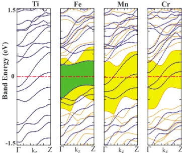
The electronic band structure of TM adsorbed H-SiNW共N兲s at ⌰=1 are shown in Figs. 8–11. We obtain different types of electronic structure depending on the type of adsorbed TM atom and N. H-SiNW共21兲+Ti is a nonmag-netic semiconductor but it is nonmagnonmag-netic metal for N = 25 and 57. For N = 21, 25, and 57, H-SiNW共N兲+Fe is ferromag-netic semiconductor with integer number of spins per primi-tive cell. It has different band gap for different spin direc-tions. In contrast, H-SiNW共21兲+Mn and H-SiNW共21兲+Cr are ferromagnetic metals with significant amounts of net magnetic moment per primitive cell.
The situation with H-SiNW共21兲+Co, H-SiNW共25兲 + Mn共Cr兲, and H-SiNW共57兲+Mn共Cr兲 共Ref.54兲 are different
from the above cases: these nanowires have half-metallic ground state. Owing to the broken spin degeneracy, energy bands, En共k,↑兲 and En共k,↓兲, split, and the nanowire remains
to be an insulator for one spin direction of electrons but becomes conductor for the opposite spin direction. The
den-TABLE III. The binding energy relative to a free TM atom EB, binding energy relative to the TM crystal EB⬘, magnetic moment per unit
cell, and minimum band gap EG共S: semiconductor, M: metal, HM: half-metal兲 of H-SiNW共N兲 covered with TM at ⌰=1 for N=21, 25, and 57. TM= Ti, Fe, Mn, Cr, and Co.
N = 21 N = 25 N = 57 EB 共eV兲 EB⬘ 共eV兲 共B兲 EG EB 共eV兲 EB⬘ 共eV兲 共B兲 EG EB 共eV兲 EB⬘ 共eV兲 共B兲 EG Ti 3.74 −1.47 0 S 4.64 −0.51 0 M 3.69 −1.46 0 M Fe 3.71 −1.07 2 S 3.52 −1.24 2 S 3.32 −1.43 2 S Mn 1.79 3.12 M 2.27 3 HM 1.82 3 HM Cr 1.81 −1.80 4.41 M 2.27 −1.34 4 HM 1.88 −1.73 4 HM Co 4.41 −0.78 1 HM 4.12 −1.07 0 M 4.08 −1.06 1 S
sity of majority- and minority-spin states, namely, D共E,↑兲 and D共E,↓兲, display a 100% spin polarization P at EF,
P =关D共EF,↑兲 − D共EF,↓兲兴/关D共EF,↑兲 + D共EF,↓兲兴. 共1兲
For the half-metallic nanowires, ⌬Em was calculated to be 0.04, 0.92, and 0.94 eV. Comparison of bands of H-SiNW共N兲 in Fig. 7 with those of H-SiNW共N兲+TM in Figs.9–11 veals that the bands gaps of H-SiNW are modified and re-duced for one spin direction. On the other hand, two or three bands of the opposite spin states cross EF and attribute a
metallicity to the nanowire. These metallic bands are com-posed of TM-3d and Si-3p hybridized states with higher TM contribution.
Half-metallic state has been a subject of interest since it was predicted first by de Groot et al.37 Initial efforts have been devoted to realize half metals using Heusler alloys or
TM-doped compound semiconductors in three-dimensional 共3D兲 crystals and in thin films.55,56 Qian et al.57 have pro-posed that half-metallic heterostructures can be formed from ␦-doped Si crystals. Recently, Son et al.58 predicted half-metallic properties of graphene nanoribbons under bias volt-age. Earlier, stable 1D half metals have been also predicted for TM atom-doped armchair single-wall carbon nanotubes59 and linear carbon chains.60
FIG. 8. 共Color online兲 Top and side views of H-SiNW共21兲 + Co 共first column兲, 共b兲 H-SiNW共25兲+Cr共Mn兲 共second column兲, and共c兲 H-SiNW共57兲+Cr共Mn兲 共third column兲.
1.5 0 -1.5 Band Energy (eV ) Ti Fe Mn Cr Co Z Γ kz Z Γ kz Z Γ kz Γ kz Z Z Γ kz
FIG. 9. 共Color online兲 Spin-polarized energy-band structures of H-SiNW共21兲 covered by TM atoms at ⌰=1. Band gaps of electrons with different spin directions are shown by different contrast. Bands described by dotted 共blue兲 and continuous 共orange兲 lines are for minority- and majority-spin states, respectively. Zero of energy is set to Fermi level.
1.5 0 -1.5 Band Energy (eV) Ti Fe Mn Cr Z Γ kz Γ kz Z Γ kz Z Γ kz Z
FIG. 10. 共Color online兲 Energy-band structures of H-SiNW共25兲 covered by TM atoms at⌰=1. Band gaps of electrons with differ-ent spin directions are shown by differdiffer-ent contrast. Bands described by dotted共blue兲 and continuous 共orange兲 lines are for minority and majority-spin states, respectively. Zero of energy is set to Fermi level. 1.5 0 -1.5 Band Energy (eV ) Ti Fe Mn Cr Z Γ kz Γ kz Z Γ kz Z Γ kz Z
FIG. 11. 共Color online兲 Energy-band structures of H-SiNW共57兲 covered by TM atoms at⌰=1. Band gaps of electrons with differ-ent spin directions are shown by differdiffer-ent contrast. Bands described by dotted共blue兲 and continuous 共orange兲 lines are for minority- and majority-spin states, respectively. Zero of energy is set to Fermi level.
As discussed in Sec. III A, we noted that the band-gap values calculated within DFT here are smaller than their ac-tual values.52At this point we address the question whether the half-metallic ground states predicted using DFT is real-istic or is an artifact. Since the present calculations predict already a band gap between occupied and unoccupied majority-spin bands, the semiconducting state should be re-alistic; the actual band gap may be larger than we predicted. As for the metallic minority-spin bands in the gap, they are reminiscent of the linear TM chain having the same lattice constant as H-SiNW共N兲+TM. The dispersion of these bands increases in the half-metallic state due to indirect TM-TM interaction via Si atoms at close proximity of adsorbed TM atom. Briefly, we believe that the present conclusion con-cerning the half-metallic state is realistic, and underestimated band gap is not affected in any essential manner as long as the optical properties of a H-SiNW+ TM is not concerned.
C. Stability of half-metallic state
Whether the half-metallic ground state is robust under de-formation is another issue we address. We found that under uniaxial compression stress the minimum of the conduction band of majority-spin states rises above EF. The minimum of
conduction band is, however, lowered under tensile stress to close the band gap. Therefore, the half-metallic state is
sen-sitive to the tensile strain for the nanowires that have the conduction-band edge close to EF. In our case, since the
conduction-band edge of H-SiNW共25兲+Cr共Mn兲 is away from EF, their half-metallic state is robust. For
H-SiNW共57兲+Cr共Mn兲 having conduction-band edge close to
EF, their semiconducting state for majority-spin bands may
transform to semimetal at high tensile strain.
Since H-SiNW+ TM nanowire is one dimension, the me-tallic minority-spin bands crossing EF are usually prone to
Peierls distortion. The form of the bands shown in Figs. 10
and11 eliminates the possibility of Peierls distortion. How-ever, H-SiNW共21兲+Co, having metallic bands crossing at
EF, can become a semiconductor for both spin direction
un-der Peierls distortion.
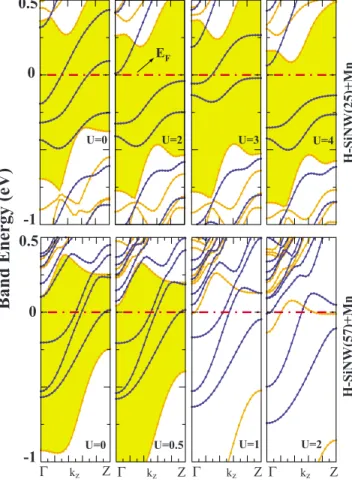
Another source of instability can be the on-site Coulomb interaction. It has been argued that the spin-dependent GGA may fail to properly represent localized 3d electrons. It may be possible that on-site repulsive Coulomb interaction de-stroys the half-metallic state. To examine the effect of on-site Coulomb repulsion, we carried out LDA+ U calculations.61 The energy-band structures of half-metallic nanowires calcu-lated for different values of U are shown in Figs.12and13. Based on this analysis, while H-SiNW共21兲+Co may not be stable and changes to ferromagnetic semiconductor even at
U = 0.5, H-SiNW共25兲+Cr共Mn兲 can keep their half-metallic
state even for U = 4. As an intermediatory situation, H-SiNW共57兲+Cr共Mn兲 can keep their half-metallic states un-til U⬃1. 0.5 0 -1 Band Energy (eV) 0.5 0 -1 0.5 0 -1 Z Γ kz Γ kz Z Γ kz Z Γ kz Z
U=0 U=0.5 U=1 U=2
U=0 U=0.5 U=1 U=2
U=0 U=2 U=3 U=4
FIG. 12. 共Color online兲 Energy-band structures of H-SiNW共N兲 covered by TM at ⌰=1 are calculated by using LDA+U method. Upper panels: Energy-band structures of H-SiNW共21兲+Co with different values of U. Middle panels: H-SiNW共25兲+Cr. Bottom panels: H-SiNW共57兲+Cr. 0.5 0.5 0 -1
Band
Energy
(eV)
0.5 0 -1U=0 U=0.5 U=1 U=2
U=0 U=2 U=3 U=4
EF H-SiNW (25 )+Mn H-SiNW(57)+Mn Z Γ kz Γ kz Z Γ kz Z Γ kz Z
FIG. 13. 共Color online兲 Energy-band structures of H-SiNW共25兲+Mn and H-SiNW共57兲+Mn calculated by using LDA+ U method.
It should be noted that the half-metallic state predicted in this study can occur in periodic and infinite structures. How-ever, the adsorption of TM atoms on a H-SiNW cannot be perfect and periodic. The size of a half-metallic H-SiNW + TM as a spintronic device has to be finite. As a result, the deviations from the perfect and periodic structures may cause the spin polarization at EF, P, to decrease from perfect value
P = 1.0. This means the destruction of ideal half metallicity.
Ideal half-metallic state can also be destroyed when ⌰⬎1. Nonetheless, even if P⬍1.0, one can still meet the require-ments for specific spintronic devices if the high spin polar-ization is achieved at EF. Here, we examined electronic and
magnetic properties of H-SiNW+ TM at high TM coverage with the objective of achieving high spin polarization at high ⌰.
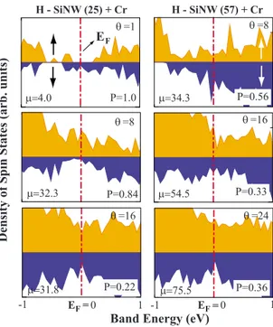
Figure 14 shows the calculated density of majority- and minority-spin states of H-SiNW共25兲 and H-SiNW共57兲 cov-ered with Cr for different values of ⌰. H-SiNW共25兲+Cr, which is a half metal with = 4B and P = 1.0 at⌰=1,
be-comes a ferromagnetic metal for both spin directions with = 32.3B and P = 0.84 at ⌰=8. Clearly, the half-metallic
state disappeared but due to the high spin polarization, this nanowire can still be used as a spintronic material. Upon increasing ⌰ to 16, spin polarization decreased to P=0.22.
EF H-SiNW共57兲+Cr at ⌰=8 has P=0.56 and = 34.3B.
The net magnetic moment per primitive cell increases to 75.5Bwhile P decreases to 0.36. It appears that P as well as
exhibit variations depending on⌰, N, and the type of TM atom. One can achieve high P by covering specific H-SiNWs with TM atoms for spintronic applications.
D. Cr doping at the interstitial site
Having analyzed the possible adsorption sites of TM at-oms on the surface of SiNW and its effects on electronic and magnetic properties, we next consider Cr atom held at an interstitial site of H-SiNW共25兲 and H-SiNW共57兲 nanowires. Such a situation can be realized when a TM atom can diffuse below the surface at high temperature. One of the possible interstitial sites is expected to be shown in Fig.15, which is close to a hollow zone. After relaxation it is found that Cr atom can settle into a cage of seven Si atoms without de-forming H-SiNW共25兲 关H-SiNW共57兲兴; their total energy is only 10共16兲 meV higher than the most energetic configura-tion obtained for the adsorpconfigura-tion of Cr to their surface but Eb
is slightly reduced and is calculated as 2.27 共1.86兲 eV. We found that the ground state of the system was to be metallic for H-SiNW共25兲 as shown in Fig. 15 with a magnetic mo-ment of 2.93B per cell. The interaction of Cr with more Si
atoms and hence the hybridization of more Cr 3d and Si 3p orbitals destroys the HM behavior and makes the wire me-tallic. When the energy-band structure in Fig.15is compared with the external counterpart, it is seen that the effects of interstitial site are more dramatic for H-SiNW共25兲, which has smaller radius. According to the band structure displayed in Fig. 15, SiNW共57兲+Cr共int兲 appears to be half-metallic
except that the highest valence band of majority spins touches the Fermi level at the Z point of the Brillouin zone. Probably, the half-metallic behavior is expected to be se-cured by GW corrections. The net magnetic moment is cal-culated to be 3.83Bper cell.
H - SiNW (25) + Cr H - SiNW (57) + Cr Dens ity o fS p in S tates (arb. un its ) P=0.84 µ=32.3 θ =8 θ =16 µ=31.8 θ =1 P=1.0 µ=4.0 θ =8 µ=34.3 θ =16 µ=54.5 θ =24 µ=75.5 -1 0 1 -1 0 1
Band Energy (eV)
EF= EF= P=0.56 P=0.33 P=0.36 P=0.22 EF
FIG. 14. 共Color online兲 Density of majority- D共E,↑兲 共dark兲 and minority- D共E,↓兲 共light兲 spin states of H-SiNW共25兲+Cr and H-SiNW共57兲+Cr for different coverage ⌰ of TM atoms 共i.e., num-ber of TM atoms per cell兲. For each case the calculated polarization
P and net magnetic moment 共in Bohr magnetons per cell兲 are
shown in corresponding panels.
1.5 0 -1.5 Band Energy (eV ) EF Z Γ kz Γ kz Z H-SiNW(57)+Cr(int) H-SiNW(25)+Cr(int)
FIG. 15. 共Color online兲 The atomic structures of the cross sec-tion of H-SiNW共25兲+Cr共int兲 and H-SiNW共57兲+Cr共int兲, where Cr is placed at the interstitial sites below the surface. Light 共orange兲 and dotted共blue兲 bands correspond to the majority- and minority-spin states.
V. CONCLUSIONS
We investigated the atomic structure, elastic, electronic, and magnetic properties of small diameter silicon nanowires oriented along 关001兴 direction. We considered bare, hydrogen-passivated, and 3d-TM 共Ti, Fe, Mn, Cr, and Co兲 decorated SiNWs. Here we summarize important predictions of our study:共i兲 the structure of ideal rods 共i.e., SiNWs hav-ing ideal bond distances and bond angles兲 cut from the bulk Si crystal undergo massive reconstruction as a result of struc-ture optimization. 共ii兲 Structure optimized bare SiNWs are generally metallic due to surface dangling bonds. At very small diameters, bare SiNWs can be a semiconductor. 共iii兲 Upon passivation of dangling bonds with hydrogen atoms, the dangling-bond surface states disappear and the metallic nanowire becomes semiconductor with sizable band gap. It has been known that due to confinement effects band gap normally increases with decreasing diameter in the range of 1–2 nm but is stabilized at a constant value for large diam-eter. It was found that this rule, however, may not be valid if the bare SiNW is relaxed before or after its passivation with hydrogen atoms. 共iv兲 The mechanical properties and hence the strength of bare SiNWs investigated in this paper vary when their surface is passivated with hydrogen atoms. Inter-estingly, squarelike cross sections are found to be slightly stronger than roundlike cross sections.共v兲 3d-TM atoms can be adsorbed on specific sites on the surface of hydrogen-passivated SiNWs with significant binding energy, and they attribute magnetic properties. At low coverage of TM atoms,
H-SiNWs become either ferromagnetic insulator or half me-tallic depending on the type of adsorbate, as well as the diameter of the nanowire. Half-metallic nanowires are insu-lators 共semiconductors兲 for one spin direction of electrons but become metal for the opposite direction of spin direction. Further analysis based on LDA+ U calculations shows that half-metallic properties are robust for specific nanowires.共vi兲 When covered with more TM atoms, the perfect half-metallic state of H-SiNW is disturbed but for certain cases, the spin polarization at EF continues to be high for
applica-tions such as spin valves. High magnetic moment obtained at high TM coverage is another remarkable result which may lead to the fabrication of nanomagnets for various applica-tions. 共vii兲 Cr atoms held at the interstitial sites below the surface give rise to metallic ferromagnetic ground state.
In conclusion, we predict that silicon nanowires can gain a wide range of interesting properties when they are func-tionalized with TM atoms, such as half metals, one-dimensional ferromagnetic semiconductors or ferromagnetic metals, and nanomagnets. Present results hold the promise for the use of silicon nanowires functionalized by 3d-transition metal atoms in nanospintronics including mag-netoresistance, spin valve, and nonvolatile memories.
ACKNOWLEDGMENT
This work has been partially supported by TUBITAK un-der Grant No. TBAG-104T536.
1For a review, see, for example, S. Ciraci, A. Buldum, and I. P.
Batra, J. Phys.: Condens. Matter 13, R537共2001兲.
2E. Durgun, R. T. Senger, H. Mehrez, S. Dag, and S. Ciraci,
Europhys. Lett. 73, 642共2006兲.
3S. Iijima, Nature共London兲 354, 56 共1991兲.
4H. Ohnishi, Y. Kondo, and K. Takayanagi, Nature共London兲 395,
780共1998兲.
5H. Dai, E. W. Wong, Y. Z. Lu, S. Fan, and C. M. Lieber, Nature
共London兲 375, 769 共1995兲; Y. Zhang and H. Dai, Appl. Phys. Lett. 77, 3015共2000兲; Y. Zhang, N. W. Franklin, R. J. Chen, and H. Dai, Chem. Phys. Lett. 331, 35共2000兲.
6S. Dag, E. Durgun, and S. Ciraci, Phys. Rev. B 69, 121407
共2004兲.
7S. Tongay, R. T. Senger, S. Dag, and S. Ciraci, Phys. Rev. Lett.
93, 136404共2004兲; S. Tongay, S. Dag, E. Durgun, R. T. Senger, and S. Ciraci, J. Phys.: Condens. Matter 17, 3823共2005兲; R. T. Senger, S. Tongay, S. Dag, E. Durgun, and S. Ciraci, Phys. Rev. B 71, 235406共2005兲, and references therein.
8P. Sen, O. Gulseren, T. Yildirim, I. P. Batra, and S. Ciraci, Phys.
Rev. B 65, 235433共2002兲.
9E. Durgun, S. Tongay, and S. Ciraci, Phys. Rev. B 72, 075420
共2005兲.
10D. P. Yu, C. S. Lee, I. Bello, X. S. Sun, Y. H. Tang, G. W. Zhou,
Z. G. Bai, Z. Zhang, and S. Q. Feng, Solid State Commun. 105, 403共1998兲.
11J. Hu, T. W. Odom, and C. M. Lieber, Acc. Chem. Res. 32, 435
共1999兲.
12K. Hiruma, M. Yazawa, T. Katsuyama, K. Ogawa, K. Haraguchi,
M. Koguchi, and H. Kakibayashi, J. Appl. Phys. 77, 447共1995兲.
13W. Q. Han, S. S. Fan, Q. Q. Li, and Y. D. Hu, Science 277, 1287
共1997兲.
14C. R. Martin, Science 266, 1961共1994兲.
15Y. F. Zhang, L. S. Liao, W. H. Chan, S. T. Lee, R. Sammynaiken,
and T. K. Sham, Phys. Rev. B 61, 8298共2000兲.
16D. D. D. Ma, C. S. Lee, F. C. K. Au, S. Y. Tong, and S. T. Lee,
Science 299, 1874共2003兲.
17M. Menon and E. Richter, Phys. Rev. Lett. 83, 792共1999兲. 18B. Marsen and K. Sattler, Phys. Rev. B 60, 11593共1999兲. 19Y. Zhao and B. I. Yakobson, Phys. Rev. Lett. 91, 035501共2003兲. 20J. D. Holmes, K. P. Johnston, R. C. Doty, and B. A. Korgel,
Science 287, 1471共2000兲.
21Y. Wu, Y. Cui, L. Huynh, C. J. Barrelet, D. C. Bell, and C. M.
Lieber, Nano Lett. 4, 433共2004兲.
22R. Rurali and N. Lorente, Phys. Rev. Lett. 94, 026805共2005兲. 23R. Q. Zhang, Y. Lifshitz, D. D. D. Ma, Y. L. Zhao, Th.
Frauen-heim, S. T. Lee, and S. Y. Tong, J. Chem. Phys. 123, 144703 共2005兲.
24P. W. Leu, B. Shan, and K. Cho, Phys. Rev. B 73, 195320
共2006兲.
25A. K. Singh, V. Kumar, R. Note, and Y. Kawazoe, Nano Lett. 6,
920共2006兲.
26Numerous theoretical studies on SiNW have been published in
Phys. Rev. Lett. 95, 167202共2005兲; Nano Lett. 5, 1587 共2005兲.
27Y. Cui, Z. Zhong, D. Wang, W. U. Wang, and C. M. Lieber,
Nano Lett. 3, 149共2003兲.
28Y. Huang, X. Duan, and C. M. Lieber, Small 1, 142共2005兲. 29X. Duan, Y. Huang, R. Agarwal, and C. M. Lieber, Nature
共Lon-don兲 421, 241 共2003兲.
30M. V. Fernandez-Serra, Ch. Adessi, and X. Blase, Phys. Rev.
Lett. 96, 166805共2006兲.
31E. Durgun, N. Akman, C. Ataca, and S. Ciraci, Phys. Rev. B 76,
245323共2007兲.
32Y. Cui, Q. Wei, H. Park, and C. M. Lieber, Science 293, 1289
共2001兲.
33X. T. Zhou, J. Q. Hu, C. P. Li, D. D. D. Ma, C. S. Lee, and S. T.
Lee, Chem. Phys. Lett. 369, 220共2003兲.
34J. Hahm and C. M. Lieber, Nano Lett. 4, 51共2004兲.
35N. Akman, E. Durgun, S. Cahangirov, and S. Ciraci, Phys. Rev.
B 76, 245427共2007兲.
36E. Durgun, D. Cakir, N. Akman, and S. Ciraci, Phys. Rev. Lett.
99, 256806共2007兲.
37R. A. de Groot, F. M. Mueller, P. G. van Engen, and K. H. J.
Buschow, Phys. Rev. Lett. 50, 2024共1983兲.
38W. E. Pickett and J. S. Moodera, Phys. Today 54共5兲, 39 共2001兲. 39H. W. Wu, C. J. Tsai, and L. J. Chen, Appl. Phys. Lett. 90,
043121共2007兲.
40M. C. Payne, M. P. Teter, D. C. Allan, T. A. Arias, and J. D.
Joannopoulos, Rev. Mod. Phys. 64, 1045共1992兲.
41Numerical computations have been carried out by using VASP
software: G. Kresse and J. Hafner, Phys. Rev. B 47, 558共1993兲; G. Kresse and J. Furthmuller, ibid. 54, 11169共1996兲.
42Charge transfer, orbital hybridization, and local magnetic
mo-ments have been obtained from SIESTAcode using local basis set: P. Ordejon, E. Artacho, and J. M. Soler, Phys. Rev. B 53, R10441共1996兲.
43W. Kohn and L. J. Sham, Phys. Rev. 140, A1133 共1965兲;
P. Hohenberg and W. Kohn, ibid. 136, B864共1964兲.
44D. Vanderbilt, Phys. Rev. B 41, 7892共1990兲.
45P. E. Blochl, Phys. Rev. B 50, 17953共1994兲.
46J. P. Perdew, J. A. Chevary, S. H. Vosko, K. A. Jackson, M. R.
Pederson, D. J. Singh, and C. Fiolhais, Phys. Rev. B 46, 6671 共1992兲.
47M. Methfessel and A. T. Paxton, Phys. Rev. B 40, 3616共1989兲. 48H. J. Monkhorst and J. D. Pack, Phys. Rev. B 13, 5188共1976兲. 49S. Ismail-Beigi and T. Arias, Phys. Rev. B 57, 11923共1998兲. 50J. X. Cao, X. G. Gong, J. X. Zhong, and R. Q. Wu, Phys. Rev.
Lett. 97, 136105共2006兲.
51R. Rurali, A. Poissier, and N. Lorente, Phys. Rev. B 74, 165324
共2006兲.
52X. Zhao, C. M. Wei, L. Yang, and M. Y. Chou, Phys. Rev. Lett.
92, 236805共2004兲.
53E. Durgun, S. Dag, V. M. K. Bagci, O. Gulseren, T. Yildirim, and
S. Ciraci, Phys. Rev. B 67, 201401共R兲 共2003兲; J. Phys. Chem. B 108, 575共2004兲.
54The obtained results are also checked for H-SiNW共45兲 which has
different facets共more round cross section兲, even though it is not more energetic than other types discussed in the paper. Cr共Mn兲 adsorption also makes H-SiNW共45兲 half-metallic with a similar band structure to H-SiNW共57兲+Cr共Mn兲.
55J.-H. Park, E. Vescovo, H.-J. Kim, C. Kwon, R. Ramesh, and
T. Venkatesan, Nature共London兲 392, 794 共1998兲.
56H. Akinaga, T. Manago, and M. Shirai, Jpn. J. Appl. Phys., Part
2 39, L1118共2000兲.
57M. C. Qian, C. Y. Fong, K. Liu, W. E. Pickett, J. E. Pask, and
L. H. Yang, Phys. Rev. Lett. 96, 027211共2006兲.
58Y.-W. Son, M. L. Cohen, and S. G. Louie, Nature共London兲 444,
347共2006兲.
59C.-K. Yang, J. Zhao, and J. P. Lu, Nano Lett. 4, 561 共2004兲;
Y. Yagi, T. M. Briere, M. H. F. Sluiter, V. Kumar, A. A. Farajian, and Y. Kawazoe, Phys. Rev. B 69, 075414共2004兲.
60S. Dag, S. Tongay, T. Yildirim, E. Durgun, R. T. Senger, C. Y.
Fong, and S. Ciraci, Phys. Rev. B 72, 155444共2005兲.
61S. L. Dudarev, G. A. Botton, S. Y. Savrasov, C. J. Humphreys,