Plasma-Enhanced Atomic Layer Deposition of III-Nitride Thin Films
C. Ozgit-Akgun, I. Donmez, and N. Biyikli
UNAM – Institute of Materials Science and Nanotechnology, Bilkent University, Bilkent, Ankara 06800, Turkey
AlN and GaN thin films were deposited by plasma-enhanced atomic layer deposition using trimethylmetal precursors. The films were found to have high oxygen incorporation, which was attributed to oxygen contamination related to the plasma system. The choice of nitrogen containing plasma gas (N2, N2/H2 or NH3) determined the severity of oxygen incorporation into deposited films. Lowest oxygen concentrations were attained for AlN and GaN thin films using NH3 and N2 plasma, respectively. Initial experiments have shown that GaN thin films with low impurity concentrations can be deposited when plasma-related oxygen contamination is avoided by the use of an alternative plasma source.
Introduction
III-nitride compound semiconductors and their alloys have emerged as promising materials for a wide range of electronic and optoelectronic device applications. Besides possessing very unique material properties individually, members of the III-nitride family with wurtzite crystal structure also exhibit direct band gaps, which cover a wide range with values of 6.2, 3.4, and 0.64 eV for AlN, GaN, and InN, respectively (1, 2). In this respect, ternary (AlxGa1-xN, AlxIn1-x N, InxGa1-xN) and quaternary alloys (AlxGayIn1-x-yN) of this family are particularly important since their bandgaps can easily be tuned by adjusting the alloy composition.
Although high quality III-nitride thin films can be grown at high temperatures (> 1000 °C) with significant rates, deposition of these films on temperature-sensitive device layers and substrates (e.g., CMOS wafers, flexible polymeric substrates, etc.) necessitates the adaptation of low-temperature methods such as atomic layer deposition (ALD). ALD is a special type of chemical vapor deposition, in which the substrate surface is exposed to sequential pulses of two or more precursors separated by purging periods. When compared to other low-temperature thin film deposition techniques, ALD stands out with its self-limiting growth mechanism, which enables the deposition of highly uniform and conformal thin films with sub-nanometer thickness control. Moreover, ternary or quaternary alloys can be easily deposited by ALD, where film composition is digitally controlled by the relative number of sub-cycles.
ALD of AlN thin films has been studied by several research groups (3-9). Lee et al. (3) reported plasma-enhanced ALD (PEALD) of AlN at 350 °C using aluminum chloride (AlCl3) and NH3/H2 plasma. Resulting AlN films were composed of microcrystallites of wurtzite (100) in an amorphous AlN matrix (4). Thermal (5, 6), plasma-enhanced (6), and
UV-assisted (7) ALD of AlN using trimethylaluminum (AlMe3) and NH3 have been studied within the temperature ranges of 320-470, 250-470, and 240-370 °C, respectively – however, no self-limiting growth behavior was observed. This was explained by Riihela et al. (5) by the fact that surface reactions between AlMe3 and NH3 occur with reasonable rates only at temperatures where AlMe3 self-decomposition takes place. Bosund et al. (8) used the same precursors to produce AlN films by PEALD at temperatures ranging from 100 to 300 °C. Films deposited in their study were amorphous except for the one grown at 300 °C. Kim et al. (9), on the other hand, have reported remote plasma ALD of amorphous AlN thin films using AlMe3 and N2/H2 plasma.
These results show that thermal ALD of AlN using AlMe3 and NH3 is not possible since these two precursors react at temperatures where AlMe3 self-decomposition takes place (5). Therefore we lowered the deposition temperatures by activating NH3 or N2/H2 through remote plasma and deposited polycrystalline wurtzite AlN thin films at temperatures ranging from 100-500 °C (10-12). Deposition parameters were optimized for these processes to achieve true ALD conditions. ALD temperature windows were observed between 100-200 °C for both processes. Films deposited at 185 °C were carbon-free and had low oxygen concentrations (< 3 at.%) although 5N-grade NH3, N2 and H2 gases were used without any further purification. Furthermore, these films were extremely smooth and showed good optical and electrical characteristics. Optical properties of these AlN thin films were investigated in detail by Alevli et al. (13). We also demonstrated conformality of the AlMe3-NH3 plasma PEALD process by fabricating high surface area AlN hollow nanofibers, which might potentially be used in high-temperature ambient chemical sensing applications (14).
When compared to AlN, significantly less number of publications focused on the ALD of GaN thin films. Growth of GaN by atomic layer epitaxy (ALE) using triethylgallium (GaEt3) (15), trimethylgallium (GaMe3) (16), and gallium trichloride (GaCl3) (17), has been reported for temperatures > 450 °C. Lower growth temperatures (350-400 °C) were achieved when GaCl was used as the gallium precursor (18). Sumakeris et al. (19) reported growth of GaN films within the temperature range of 150-650 °C by using a novel reactor design that employs hot filaments to decompose the ammonia. Kim et al. (20) deposited GaN thin films by thermal ALD using GaCl3 and NH3 precursors.
Our initial efforts on depositing GaN thin films using GaMe3 or GaEt3 with NH3 plasma resulted in amorphous thin films with high oxygen concentrations (~20 at.%) (21, 22). Several experiments were carried out in order to determine the source of oxygen present in these films, and the most probable source was presumed as the oxygen impurities in the 5N-grade NH3 gas. However, this argument has failed when the same GaN deposition was repeated with the purified process gases. The true source of oxygen contamination was then found to be the quartz tube of the inductively coupled plasma source itself. Such plasma-related oxygen contamination was also reported for GaN thin films grown by remote plasma enhanced chemical vapor deposition (23).
In this report we review our previous and current efforts on the development of PEALD processes for III-nitrides, and present detailed characterization results for the deposited AlN and GaN thin films.
Experimental Details
Substrate Cleaning
Prior to depositions, Si (100) or Si (111) substrates were cleaned by sequential ultrasonic agitation in 2-propanol, acetone, methanol, and deionized (DI) water. Substrates were then dipped into dilute hydrofluoric acid solution (5 vol.% HF) to remove the surface native oxide for ~ 1-2 min, then rinsed with DI water and dried with N2.
Deposition of Thin Films
Films were deposited on pre-cleaned substrates at temperatures ranging from 185 to 215 °C. Depositions were carried out in a Fiji F200-LL ALD reactor equipped with an inductively coupled RF-plasma source (Ultratech/CambridgeNanoTech Inc.). Trimethylaluminum (AlMe3) and trimethylgallium (GaMe3) were used for the deposition of AlN and GaN thin films, respectively. AlMe3 was kept at room temperature, whereas GaMe3 was cooled down to 6 °C using a home-made Peltier cooling system. 5N-grade NH3, N2 and H2 plasma gases, and the carrier gas, Ar, were further purified using MicroTorr gas purifiers. Base pressure was ~150 mTorr. Remote plasma was activated at each cycle during the introduction of N-containing plasma gas. System was purged for 10 s after each exposure.
Characterization of Thin Films
Ellipsometric spectra were recorded in the wavelength range of 300-1000 nm for AlN and 400-1200 nm for GaN thin films at three angles of incidence (65°, 70°, and 75°) using a variable angle spectroscopic ellipsometer (J.A. Woollam). Thicknesses of the films were then obtained by modeling the measured data using Cauchy dispersion function. Chemical compositions of the films were determined by X-ray photoelectron spectroscopy (XPS) using Thermo Scientific K-Alpha spectrometer with a monochromatized Al Kα X-ray source. Etching of the samples was carried out with a beam of Ar ions having an acceleration voltage and spot size of 1 kV and 400 µm, respectively. Data were corrected for charging by shifting peaks with respect to C 1s or Ar 2p. X-ray reflectivity (XRR) and grazing-incidence X-ray diffraction (GIXRD) measurements were carried out in a PANalytical X'Pert PRO MRD diffractometer using Cu Kα radiation. GIXRD patterns were obtained by performing 10 repeated scans within the 2Theta range of 20-80° with a step size of 0.1° and counting time of 10 s. These scans were then added together in order to obtain a single GIXRD pattern with good intensity values.
Results and Discussion
Deposition of GaN using NH3, N2 and N2/H2 plasma
Three samples were deposited at 185-215 °C using different N-containing plasma gases, namely NH3, N2, and N2/H2. During these experiments load lock of the PEALD system was temporarily disabled. Therefore, samples were loaded to the reactor through
the gate while the reactor was at atmospheric pressure. The gate was then closed using a custom-made aluminum lid and the reactor was evacuated. Reactor was baked out at 250 °C for ~18 h before each deposition.
For the film deposited with NH3 plasma, one PEALD cycle consisted of 0.015 s GaMe3 (Tprecursor = 6 °C)/10 s Ar purge/50 sccm, 90 s, 300 W NH3 plasma /10 s Ar purge. For this sample, 21.5 at.% oxygen was detected in the bulk film using ex situ X-ray photoelectron spectroscopy (XPS). In other words, the high oxygen concentration in GaN film could not be lowered by the use of purified process gases. It has been then realized that the actual source of this oxygen contamination was the etching of quartz tube in which plasma forms. For the following depositions, shorter plasma durations were used in order to avoid heating of the quartz tube and therefore minimize the sputtering of quartz. Table I summarizes the deposition conditions for GaN thin film samples. Elemental compositions of the deposited films are given in Table II.
TABLE I. Deposition details for GaN thin film samples. Plasma Gas Flow Rate
(sccm) Flow Duration (s) Deposition Temperature (°C) Number of Cycles Film Thickness (nm) NH3 50 90 185 1000 31.6 N2 50 20 215 1000 19.1 N2/H2 50/20 20/5 200 1000 22.0
TABLE II. Elemental compositions of GaN thin film samples as determined by XPS survey scans. Data were collected after 60 s Ar ion etching.
Plasma Gas Ga/N O (at.%) C (at.%) Ar (at.%)
NH3 1.42 21.46 0.00 1.84
N2 1.07 4.48 9.12 0.00
N2/H2 1.04 4.70 4.20 0.00
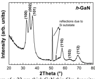
When N2 plasma was used instead of the NH3 plasma, oxygen concentration of GaN thin film decreased to 4.5 at.%, whereas its carbon concentration increased to 9.1 at.%. The sample deposited using N2 plasma was amorphous. We were able to deposit polycrystalline wurtzite GaN thin films with low oxygen and carbon concentrations (4.7 and 4.2 at.%, respectively) at 200 °C by introducing 20 sccm H2 in addition to 50 sccm N2 during the third quarter of the plasma duration. GIXRD pattern of the GaN film deposited using N2/H2 plasma is shown in Figure 1. These results show that carbon impurities have a detrimental effect on the crystallinity of GaN and introduction of H2 during the N2 plasma is crucial for achieving carbon-free III-nitride thin films.
Film thickness values obtained by fitting of the measured X-ray reflectivity (XRR) data were slightly lower than those measured by spectroscopic ellipsometry. Density values of 4.64, 4.09 and 4.91 g/cm3, and roughness values of 0.49, 1.16 and 2.61 nm were found for GaN films deposited using NH3, N2 and N2/H2 plasmas, respectively, using XRR.
Figure 1. GIXRD pattern of a 22 nm-thick GaN thin film deposited at 200 °C by PEALD using GaMe3 and N2/H2 plasma.
Deposition of AlN using NH3, N2 and N2/H2 plasma
Six samples were deposited at 190 °C using different N-containing plasma gases, namely NH3, N2, and N2/H2. During these experiments load lock of the PEALD system was temporarily disabled. Therefore, samples were loaded to the reactor through the gate while the reactor was at atmospheric pressure. The gate was then closed using a custom-made aluminum lid and the reactor was evacuated. Reactor was baked out at 250 °C for ~12 h prior to each deposition. After these bake outs, the lowest vacuum value measured was 8.2 x 10⁻⁶ Torr at 190 °C. One PEALD cycle was consisted of 0.1 s AlMe3/10 s Ar purge/N-containing plasma (plasma power = 300 W)/10 s Ar purge. Deposition details for AlN thin film samples are summarized in Table III. Elemental compositions of the deposited AlN films are given in Table IV.
TABLE III. Deposition details for AlN thin film samples. Plasma Gas (-Sample Number) Flow Rate (sccm) Flow Duration (s) Deposition Temperature (°C) Number of Cycles Film Thickness (nm) NH3 50 20 190 500 33.5 N2 50 20 190 500 53.1 N2/H2-1 50/20 20/5 (H2 at 3rd quarter) 190 500 42.9 N2/H2-2 50/20 20/5 (H2 at 1st quarter) 190 500 53.8 N2/H2-3 50/50 20 190 500 17.1 N2/H2-4 50/20 20 190 500 20.4
TABLE IV. Elemental compositions of AlN thin film samples as determined by XPS survey scans. Plasma Gas Etch Time (s) Al/N O (at.%) C (at.%) Ar (at.%)
NH3 150 1.25 1.51 3.88 1.90 N2 150 4.51 48.45 8.00 1.07 N2/H2-1 150 5.55 45.71 6.44 1.83 N2/H2-2 150 5.02 47.42 7.72 1.38 N2/H2-3 50 1.27 4.04 4.95 2.02 N2/H2-4 50 1.28 4.73 5.94 1.93
In the case of GaN thin films, the film deposited using NH3 plasma had ~20 at.% O in the bulk film. The use of N2 or N2/H2 plasma decreased this value to < 5 at.%. When
same approach was followed for the deposition of AlN using AlMe3, oxygen concentration of the film increased tremendously (i.e. > 45 at.%). AlN samples deposited using N2/H2 plasma process, in which N2 and H2 are simultaneously introduced into the reactor, had 4-5 at.% O and 5-6 at.% C in the bulk film. For AlN, best results were obtained with the AlMe3-NH3 plasma process. For this sample, 3.9 at.% C was found in the bulk film. In our previous work (10), we reported on the deposition of carbon-free AlN thin films with low oxygen concentrations using the same PEALD process. This suggests that NH3 plasma duration (20 vs. 40 s) has a major effect on the resulting carbon concentration of AlN thin films. Samples with high oxygen concentrations were amorphous as determined by GIXRD. Samples N2/H2-3 and N2/H2-4 were also amorphous due to the O (~4-5 at.%) and C (~5-6 at.%) impurities. The sample deposited using NH3 plasma had lower impurity concentrations. Its GIXRD pattern revealed a weak crystallinity with broad peaks corresponding to the hexagonal wurtzite crystal structure. XRR data were fitted using a three-layer model, i.e. Si/SiO2/AlxOyNz, for the films having > 45 at.% O. For the AlN films with low O concentrations, on the other hand, a four-layer model, i.e. Si/SiO2/AlN/Al2O3, has been applied. XRR results are given in Table V.
TABLE V. Thickness, density and roughness values for AlN thin film samples as determined by XRR. Plasma Gas tAlN or tAlxOyNz tAl2O3 (nm) ρ (g/cm3) Rrms (nm)
NH3 31.69 0.35 2.49 1.01 N2 50.98 - 2.48 0.28 N2/H2-1 41.52 - 2.53 0.71 N2/H2-2 51.64 - 2.51 0.51 N2/H2-3 15.94 1.36 2.42 0.85 N2/H2-4 17.44 2.05 2.35 0.59
Initial Results Obtained with the Hollow Cathode Plasma Source
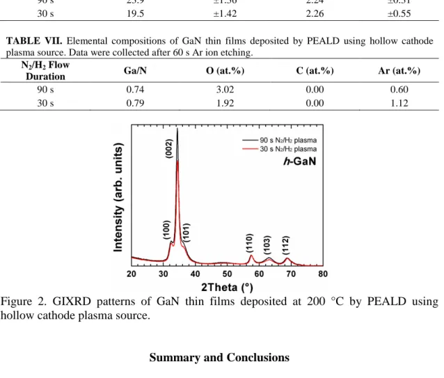
We replaced the inductively coupled RF-plasma source of the Fiji F200-LL ALD reactor with a stainless steel hollow cathode plasma source (MEAglow Ltd.). Prior to depositions, system was baked out at 250 °C for ~12-24 h. Pre-cleaned, HF-dipped 4” Si (100) wafers were then introduced to the reactor via load lock. 800 GaN cycles were deposited at 200 °C using GaMe3 and N2/H2 plasma, where one cycle consisted of 0.015 s GaMe3 (TPrecursor = 6 °C)/10 s Ar purge/ 50 + 50 sccm, 30 or 90 s, 300 W N2/H2 plasma/ 10 s Ar purge. Table VI summarizes spectroscopic ellipsometry results obtained from these GaN thin film samples. Spectroscopic ellipsometry measurements were taken from 5 different points on the 4” Si wafer (center and edges). Using the results of these measurements, average thickness and average refractive index values were obtained. Uniformity of thickness and refractive index across the 4” wafer were also calculated and presented in Table VI. Elemental compositions of the GaN films were revealed using XPS (see Table VII). Deposited GaN films were carbon-free and had very low oxygen concentrations. Since residual water vapor on the walls of the chamber decay with each metalorganic pulse, oxygen concentration in the bulk film, which was determined as 3.02 at.% for the first GaN deposition, decreased to 1.92 at.% for the following deposition. GIXRD patterns of these GaN thin films are given in Figure 2. Both samples were polycrystalline and exhibited hexagonal wurtzite crystal structure.
TABLE VI. Thickness and refractive index values for GaN thin films deposited by PEALD using hollow cathode plasma source.
N2/H2 Flow Duration Average Thickness (nm) Uniformity of Thickness (%) Average Refractive Index Uniformity of Refractive Index (%) 90 s 23.9 ±1.36 2.24 ±0.31 30 s 19.5 ±1.42 2.26 ±0.55
TABLE VII. Elemental compositions of GaN thin films deposited by PEALD using hollow cathode plasma source. Data were collected after 60 s Ar ion etching.
N2/H2 Flow
Duration Ga/N O (at.%) C (at.%) Ar (at.%)
90 s 0.74 3.02 0.00 0.60
30 s 0.79 1.92 0.00 1.12
Figure 2. GIXRD patterns of GaN thin films deposited at 200 °C by PEALD using hollow cathode plasma source.
Summary and Conclusions
AlN and GaN depositions were carried out using trimethylmetal precursors in the presence of plasma-related oxygen contamination. In the case of AlN thin films, lowest oxygen concentrations were obtained using NH3 plasma (~1.5 at.%). Oxygen concentration in AlN films increased tremendously (i.e. > 45 at.%) when N2 or certain N2/H2 plasma processes were used. PEALD processes designed for GaN, on the other hand, showed an adverse response to the use of NH3, N2, and N2/H2 plasma gases in terms of oxygen incorporation. Film deposited using NH3 plasma had ~20 at.% O in the bulk film. The use of N2 or N2/H2 plasma decreased this value to < 5 at.%. These results suggest that the severity of oxygen incorporation into AlN and GaN thin films are being determined by the choice of nitrogen containing plasma gas. However, this choice is highly precursor dependent and might not be anticipated for other PEALD processes. Initial results showed that polycrystalline wurtzite GaN thin films with low impurity contents can be deposited when the plasma-related oxygen contamination is avoided using a hollow cathode plasma source. Efforts are underway to optimize PEALD process parameters for III-nitride thin films and their ternary alloys.
Acknowledgments
This study was supported by the State Planning Organization (DPT) of Turkey through the National Nanotechnology Research Center (UNAM) Project. Authors acknowledge M. Sowa from Ultratech/CambridgeNanoTech Inc. and S. Butcher from MEAglow Ltd. for their useful comments and suggestions. C. Ozgit-Akgun acknowledges TUBITAK-BIDEB for National PhD Fellowship. N. Biyikli acknowledges support from Marie Curie International Reintegration Grant (Grant # PIRG05-GA-2009-249196) and TUBITAK (Project # 112M004 and 112M482).
References
1. S. C. Jain, M. Willander, J. Narayan, and R. Van Overstraeten, J. Appl. Phys., 87, 965 (2000).
2. J. Wu, J. Appl. Phys., 106, 011101 (2009).
3. Y. J. Lee and S.-W. Kang, Thin Solid Films, 446, 227 (2004). 4. Y. J. Lee, J. Cryst. Growth, 266, 568 (2004).
5. D. Riihela, M. Ritala, R. Matero, M. Leskela, J. Jokinen, and P. Haussalo, Chem.
Vap. Deposition, 2, 277 (1996).
6. X. Liu, S. Ramanathan, E. Lee, and T. E. Seidel, Mater. Res. Soc. Symp. Proc.,
811, D1.9 (2004).
7. D. Eom, S. Y. No, C. S. Hwang, and H. J. Kim, J. Electrochem. Soc., 153, C229 (2006).
8. M. Bosund, T. Sajavaara, M. Laitinen, T. Huhtio, M. Putkonen, V.-M. Airaksinen, and H. Lipsanen, Appl. Surf. Sci., 257, 7827 (2011).
9. K.-H. Kim, N.-W. Kwak, and S. H. Lee, Electron. Mater. Lett., 5, 83 (2009). 10. C. Ozgit, I. Donmez, M. Alevli, and N. Biyikli, Thin Solid Films, 520, 2750
(2012).
11. M. Alevli, C. Ozgit, I. Donmez, and N. Biyikli, Phys. Status Solidi A, 209, 266 (2012).
12. M. Alevli, C. Ozgit, I. Donmez, and N. Biyikli, J. Cryst. Growth, 335, 51 (2011). 13. M. Alevli, C. Ozgit, I. Donmez, and N. Biyikli, J. Vac. Sci. Technol. A, 30,
021506 (2012).
14. C. Ozgit-Akgun, F. Kayaci, I. Donmez, T. Uyar, and N. Biyikli, J. Am. Ceram.
Soc., 96, 916 (2013).
15. M. A. Khan, R. A. Skogman, J. M. Van Hove, D. T. Olson, and J. N. Kuznia,
Appl. Phys. Lett., 60, 1366 (1992).
16. N. H. Karam, T. Parodos, P. Colter, D. McNulty, W. Rowland, J. Schetzina, N. El-Masry, and S. M. Bedair, Appl. Phys. Lett., 67, 94 (1995).
17. H. Tsuchiya, M. Akamatsu, M. Ishida, and F. Hasegawa, Jpn. J. Appl. Phys., 35, L748 (1996).
18. A. Koukitu, Y. Kumagai, T. Taki, and H. Seki, Jpn. J. Appl. Phys., 38, 4980 (1999).
19. J. Sumakeris, Z. Sitar, K. S. Ailey-Trent, K. L. More, and R. F. Davis, Thin Solid
Films, 225, 244 (1993).
20. O. H. Kim, D. Kim, and T. Anderson, J. Vac. Sci. Technol. A, 27, 923 (2009). 21. C. Ozgit, I. Donmez, M. Alevli, and N. Biyikli, J. Vac. Sci. Technol. A, 30,
22. C. Ozgit, I. Donmez, M. Alevli, and N. Biyikli, Acta Phys. Pol. A, 120, A-55 (2012).
23. K. S. A. Butcher, Afifuddin, P. P.-T. Chen, and T. L. Tansley, Phys. Status Solidi