ENVELOPE TRACKING RF POWER
AMPLIFIER DESIGN
a thesis submitted to
the graduate school of engineering and science
of bilkent university
in partial fulfillment of the requirements for
the degree of
master of science
in
electrical and electronics engineering
By
Mustafa Engin Estekin
May 2020
ENVELOPE TRACKING RF POWER AMPLIFIER DESIGN By Mustafa Engin Estekin
May 2020
We certify that we have read this thesis and that in our opinion it is fully adequate, in scope and in quality, as a thesis for the degree of Master of Science.
Abdullah Atalar(Advisor)
Ergin Atalar
Ali Bozbey
Approved for the Graduate School of Engineering and Science:
ABSTRACT
ENVELOPE TRACKING RF POWER AMPLIFIER
DESIGN
Mustafa Engin Estekin
M.S. in Electrical and Electronics Engineering Advisor: Abdullah Atalar
May 2020
In modern wireless communication systems, the requirement of achieving high data rates results in non-constant envelope signals with high peak to average power ratio (PAPR). However, the operation of conventional power amplifiers (PAs) at back-off power levels creates significant degradation in efficiency. Since efficiency is a critical design consideration for PAs to avoid high power consump-tion and heating problems, several techniques were introduced to maintain the high efficiency for a wide range of power levels.
We designed an envelope tracking power amplifier (ETPA) that uses the supply modulation technique which is a promising solution to the efficiency degradation problem. In ETPA, the high efficiency is maintained at back-of levels by adjusting the supply voltage in accordance with the time varying signal envelope. The supply voltage was efficiently generated by using a synchronous buck converter operating at 10 MHz switching frequency. The converter was integrated to the designed class-AB PA by using a proper low pass filter. In order to improve the signal bandwidth that can be tracked, an envelope bandwidth elimination algorithm was used. The efficiency of the resulting ETPA system was measured as 26% for the signal that has 3 MHz bandwidth and 12 dB PAPR. The system has an efficiency of 20% with the signal that has 5 MHz bandwidth and 13 dB PAPR.
Keywords: Supply modulation, envelope tracking, power amplifier, back-off effi-ciency enhancement.
¨
OZET
ZARF TAK˙IP METODU RADYO FREKANS G ¨
UC
¸
Y ¨
UKSELTEC˙I TASARIMI
Mustafa Engin Estekin
Elektrik-Elektronik M¨uhendisli˘gi, Y¨uksek Lisans Tez Danı¸smanı: Abdullah Atalar
Mayıs 2020
Modern kablosuz ileti¸sim sistemlerinde, y¨uksek veri hızlarına ula¸sma gereksinimi sebebiyle y¨uksek tepe - ortalama g¨u¸c oranına sahip de˘gi¸sken zarflı sinyaller kullanılır. Bununla birlikte, geleneksel g¨u¸c y¨ukselte¸clerin maksimum g¨u¸c seviyelerinin ¸cok gerisinde ¸calı¸sması, verimlilikte ¨onemli bir bozulma yaratır. Verimlilik, y¨uksek g¨u¸c t¨uketimi ve ısınma sorunlarından ka¸cınmak i¸cin kritik bir tasarım de˘gerlendirmesi oldu˘gundan, y¨uksek verimlili˘gi geni¸s bir g¨u¸c seviyesi aralı˘gında korumak i¸cin ¸ce¸sitli teknikler uygulanmaktadır.
Bu ¸calı¸smada d¨u¸s¨uk verimlilik sorununa ¸c¨oz¨um olarak, bir besleme mod¨ulasyonu tekni˘gi olan zarf takibi metodu g¨u¸c y¨ukseltecin tasarımı sunulmu¸stur. Besleme voltajı, zamana g¨ore de˘gi¸sen sinyal zarfına g¨ore ayarla-narak y¨uksek verimlilik maksimum g¨u¸c seviyelerinin gerisinde de korunmu¸stur. Besleme voltajı, 10 MHz anahtarlama frekansında ¸calı¸san bir senkron buck d¨on¨u¸st¨ur¨uc¨u kullanılarak verimli bir ¸sekilde ¨uretilmi¸stir. D¨on¨u¸st¨ur¨uc¨u, uygun bir al¸cak ge¸ci¸s filtresi kullanılarak, AB-sınıfında tasarlanmı¸s g¨u¸c y¨ukseltece entegre edilmi¸stir. Takip edilebilecek sinyal bant geni¸sli˘gini artırmak amacıyla bir zarf bant geni¸sli˘gi eleme algoritması kullanılmı¸stır. Tasarlanan sistemin verimlili˘gi, 3 MHz bant geni¸sli˘gi ve 12 dB tepe - ortalama g¨u¸c oranına sahip sinyal i¸cin %26 olarak ¨ol¸c¨ulm¨u¸st¨ur. 5 MHz bant geni¸sli˘gi ve 13 dB tepe - ortalama g¨u¸c oranına sahip sinyal i¸cin sistem, %20’lik bir verimle ¸calı¸smaktadır.
Anahtar s¨ozc¨ukler : Besleme mod¨ulasyonu, zarf takibi, g¨u¸c y¨ukselteci, d¨u¸s¨uk-g¨u¸c verimi artırma.
Acknowledgement
I would like to express my sincere gratitude to my advisor Prof. Abdullah Atalar for his continuous guidance and support during my MS study. Prof. Atalar will always be an inspiration to me with his exemplary personality, endless moti-vation and immense knowledge.
I am also thankful to Prof. Ergin Atalar and Assoc. Prof. Ali Bozbey for being part of the thesis committee.
I would also like to thank my research mates in Prof. Atalar’s group, Erdem Aras, Cem B¨ulb¨ul and C¸ a˘gda¸s Ballı for the helpful discussions during the research meetings.
I would like to thank all my superiors and colleagues in Microwave Design Division at Meteksan Defence Ind. Inc. for their valuable support since the beginning of my professional life. The technical and physical support of Meteksan Defence Ind. Inc. is also greatly appreciated.
Finally, I owe special thanks to my beloved family that always encourages and supports me throughout my life. This accomplishment would not have been possible without their support.
Contents
1 Introduction 1
1.1 Motivation . . . 1
1.2 Thesis Outline . . . 3
2 Background 4 2.1 RF Power Amplifier Basics . . . 4
2.2 Back-Off Efficiency Enhancement Techniques . . . 6
2.3 Envelope Tracking Power Amplifier Systems . . . 7
2.4 Literature Research . . . 9
3 Design of the Envelope Amplifier 11 3.1 Fundamentals of Power MOSFETs and Buck Converters . . . 11
3.2 Synchronous Buck Converter Design . . . 15
3.3 Output Stage Filter Design . . . 18
CONTENTS vii
4 Design of the RF Power Amplifier 22
4.1 Class AB Power Amplifier Design . . . 22 4.2 Simulation Results . . . 28 4.3 Measurement Results . . . 30
5 Slow Tracking and Supply Signal Generation 33
5.1 Envelope Bandwidth Elimination . . . 33 5.2 Supply Signal Generation . . . 35
6 Measurement 39
6.1 AM Signal Measurement . . . 39 6.2 LTE Signal Measurement . . . 42
List of Figures
2.1 Overhead Voltages in Constant Supply and Envelope Tracking
Sys-tems . . . 7
2.2 Envelope Tracking RFPA System . . . 8
3.1 Buck Converter Topologies . . . 12
3.2 Parasitic Elements of a MOSFET . . . 13
3.3 Voltage and Current Waveforms During Turn On . . . 14
3.4 Bootstrap Topology . . . 16
3.5 Filter Schematics . . . 19
3.6 Low Pass Filter Topology . . . 19
3.7 Frequency Responses of the Filters . . . 20
3.8 Measured Efficiency of the Envelope Amplifier for 10 MHz (Blue) and 20 MHz (Red) . . . 21
4.1 Power Amplifier Circuit . . . 23
LIST OF FIGURES ix
4.3 Load Pull Simulation . . . 25
4.4 Input Matching Circuit . . . 25
4.5 Output Matching Circuit . . . 26
4.6 RFPA Layout . . . 26
4.7 Layout of the ET RFPA Circuit . . . 27
4.8 S-Paratemer Simulation . . . 28
4.9 K Factor Simulation . . . 29
4.10 Output Power and PAE Simulation . . . 29
4.11 S-Parameter Measurement . . . 30
4.12 Output Power and PAE Measurement . . . 31
4.13 Gain Measurement . . . 31
4.14 Photograph of the Fabricated Circuit . . . 32
5.1 Real Envelope and Slew Rate Limited Version in Time Domain . 35 5.2 Real Envelope and Slew Rate Limited Version in Frequency Spectrum 36 5.3 CDF of the Supply Signal . . . 37
5.4 Discrete Mapping and Quadratic Interpolation . . . 38
6.1 Measurement Setup . . . 39
6.2 Modulated Signal Envelope and Supply Voltage Generated for AM Measurement . . . 40
LIST OF FIGURES x
6.3 AM Signal (Yellow) and Supply Voltage Waveform (Green) . . . . 41 6.4 Measured Output Power Spectrum of ET RFPA by Using the AM
Signal . . . 41 6.5 LTE Signal (Yellow) and Supply Voltage Waveform (Green) . . . 42 6.6 Measured Output Power Spectrum of ET RFPA . . . 43
List of Tables
1.1 Features of Modern Communication Standards . . . 2
3.1 High Power Switching Transistors . . . 16
5.1 Lookup Table of the Peak Efficiency Points . . . 36
6.1 Summary of the Efficiency Performance in AM Measurement . . . 41 6.2 Summary of the Efficiency Performance in LTE Measurement . . 42
Chapter 1
Introduction
1.1
Motivation
RF power amplifiers are widely used devices in wireless communication systems and radars to deliver RF power to the antennas. Since they are highly energy dissipating devices, the power amplifiers have significant roles in the overall trans-mitter efficiency. To minimize the energy consumption, improve the battery life of the portable devices and avoid heating problems, efficiency is an important design consideration.
Early wireless systems such as Advanced Mobile Phone Systems and Global System for Mobile used constant envelope modulation techniques in which the information is carried on the phase and frequency [1]. In these systems, the RFPAs are designed to operate in their most efficient mode, since the linearity is not the main concern.
With the development of communication technologies, the number of the wire-less communication devices and the quantity of data increased dramatically. Since the frequency spectrum allocated for the wireless systems essentially remained the same, efficiently usage of the spectrum became more important. Therefore, more
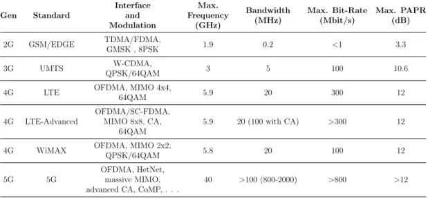
complex modulation techniques were developed to obtain high data rates for the available and expensive bandwidths. Some features of modern mobile communi-cation standards are displayed in Table 1.1 [2].
Table 1.1: Features of Modern Communication Standards
Gen Standard Interface and Modulation Max. Frequency (GHz) Bandwidth (MHz) Max. Bit-Rate (Mbit/s) Max. PAPR (dB) 2G GSM/EDGE TDMA/FDMA, GMSK , 8PSK 1.9 0.2 <1 3.3 3G UMTS W-CDMA, QPSK/64QAM 3 5 100 10.6 4G LTE OFDMA, MIMO 4x4,
64QAM 5.9 20 300 12 4G LTE-Advanced OFDMA/SC-FDMA, MIMO 8x8, CA, 64QAM 5.9 20 (100 with CA) >300 12 4G WiMAX OFDMA, MIMO 2x2,
QPSK/64QAM 5.8 20 100 12 5G 5G
OFDMA, HetNet, massive MIMO, advanced CA, CoMP, . . .
40 >100 (800-2000) >800 >12
The non-constant envelope modulation techniques such as QPSK, W-CDMA and OFDM are very popular in modern wireless systems to use the spectrum more efficiently [3]. For these non-constant envelope signals, the peak to average power ratio (PAPR) is a measure of how different signal amplitude levels the signal contains. High data rates can be achieved by using high PAPR signals. In these systems, both linearity and efficiency need to be satisfied for a wide range of power levels. However, the conventional classes of PAs are designed to operate efficiently for the nearly saturated power levels. The efficiency reduces at the back off power levels because full rail to rail voltage swing is not maintained.
The existing solutions to the efficiency degradation includes load modulation and supply modulation techniques which are based on dynamical adjustment of the load line. Outphasing amplifiers [4–6], Doherty amplifiers [7–9] and load modulated balanced amplifiers [10, 11] are the examples of the load modulation techniques. On the other hand, supply modulation techniques include envelope elimination and restoration (EER) [12,13] and envelope tracking power amplifiers (ETPA) [14, 15].
In this study, the aim is to design an envelope tracking power amplifier that can be operated efficiently under the high PAPR signals used by the modern wireless communication technologies. The high efficiency will be maintained for a wide range of power levels by enhancing the back-off efficiency. The design will be fabricated and verified for auxiliary LTE signals.
1.2
Thesis Outline
Chapter 2 explains the basics of RF power amplifiers and back-off efficiency en-hancement techniques. Envelope tracking concept and the literature review are presented.
In Chapter 3, a detailed explanation of the envelope amplifier is given. Starting from the important parameters of a power MOSFET, design of the converter and the output filter are explained. In Chapter 4, the design steps of the RF power amplifier and the constant supply measurement results are presented.
Chapter 5 presents the slow tracking concept. The envelope bandwidth elimi-nation algorithm that is applied to the system is explained. In this chapter, the supply signal is generated by mapping RF input power levels to proper supply voltages.
In Chapter 6, the efficiency and linearity performances of the fabricated enve-lope tracking power amplifier are measured by using AM and LTE signals. The results are compared to the constant supply systems. Lastly, Chapter 7 includes the conclusion of the thesis.
Chapter 2
Background
2.1
RF Power Amplifier Basics
In an RF transmitter signal chain, RF power amplifier is the device that drives the antenna by boosting the power of the RF signal to the level necessary for the design. Since it has a key role in the RF transmitter performance, there are strong requirements of an RFPA such as output power, linearity, energy efficiency and cost.
The efficiency of the RFPA is the measure of its ability to convert the DC power to RF signal power delivered to the antenna. Because of the limited efficiency of RFPAs, only some of the DC power can be converted to RF power. The DC power that is not converted to RF signal power is dissipated as heat. Since RFPAs are generally most energy consuming components of the transmitter, efficiency is a critical design consideration for the devices such as portable devices and satellites that have limited power sources. Due to the cooling problems, the efficiency is also important for the systems in which the power consumption is not the main issue.
For an ideal linear amplifier, the output power increases linearly with the in-creasing input power. However, gain of a real power amplifier does not stay constant for all power levels. The nonlinearity behavior changes the signal char-acteristics and creates distortion on the signal. For the modulation techniques in which the information is carried on the frequency or the phase, the input RF signal has a constant envelope. In this case, linear amplitude transmission is not required, hence the linearity is not the main issue. On the other hand, the RF envelope is non-constant for the more adaptive modulation techniques that allow higher data rates. OFDM, QPSK and QAM are the examples of the non-constant envelope modulations, and they require linear amplitude transmission. Therefore, linearity of the RFPA is critical for these modulation techniques.
In order to achieve different specifications, RFPAs are designed with different modes of operation called classes. Class-A, class-AB and class-B are called linear mode amplifiers that use the transistor as a voltage controlled source. In linear mode amplifiers, the class is determined by the bias condition applied to the transistor. The bias condition controls the conduction angle which is defined as the duration of the period in which the transistor is conducting.
In addition to the linear amplifier classes, the other mode of operation is called switching-mode classes. In switching mode classes such as class D, class E and class F, the transistor is overdriven and operates as a switch instead of a current source. Using these classes, higher efficiencies can be obtained for narrowband operations with a high nonlinearity.
The conventional classes cannot provide high efficiency and good linearity at the same time. In order to have good linearity, the amplifier can be operated with small input power levels. However, the efficiency drops significantly at back-off power levels. On the other hand, the amplifier is efficient but nonlinear at the power levels near saturation.
2.2
Back-Off
Efficiency
Enhancement
Tech-niques
In modern wireless communication systems, non-constant envelope modulation techniques such as QPSK, W-CDMA and OFDM are widely used to increase the spectrum efficiency. In these modulation techniques, signals designed for high data rates result in high peak-to-average power ratio (PAPR) waveforms.
However, the conventional RF power amplifiers are designed to operate effi-ciently at the power levels near compression, and the high efficiency is not main-tained for back-off power levels. The drain efficiency of a PA can be written in terms of the load impedance RL, the fundamental frequency current Ids and DC
voltage and current components VDS and IDS, as given in Eqn. 2.1. Since IDS
and Ids change in proportional to the drive power level, the efficiency at the low
drive levels is degraded. The overall efficiency drops in the case of non-constant RF envelope with high PAPR because of the inefficient operation at the back-off levels. η = Pout PDC = RloadI 2 ds 2VDSIDS (2.1)
In order to maintain the high efficiency at a large range of power levels, different methods have been implemented. The two popular methods to enhance the back-off efficiency are load modulation and supply modulation that are based on dynamical adjustment of the load line.
In load modulation methods, the load impedance is adjusted inversely pro-portional to the drive level. Thus, the high efficiency is maintained for different drive levels. Doherty PA, varactor based load modulation, chireix outphasing and load modulated balanced amplifiers are the popular examples of dynamic load modulation.
the VDS in proportional to the drive level. Envelope elimination and restoration
(EER) and envelope tracking (ET) are the examples of dynamic supply modula-tion techniques.
2.3
Envelope Tracking Power Amplifier
Sys-tems
Envelope tracking is one of the dynamical supply modulation methods to enhance the back-off efficiency. The envelope tracking theory suggests that full rail-to-rail voltage swing in the power amplifier can be maintained by adjusting the supply voltage in accordance with the time varying signal envelope. In this case, the PA is kept near compression for different RF power levels. Thus, the overhead voltage is kept minimum and the maximum efficiency is maintained. Figure 2.1 illustrates the overhead voltages during the amplification of a non-constant envelope signal for constant supply voltage and ET system.
(a) Constant Supply Voltage (b) Envelope Tracking
Figure 2.1: Overhead Voltages in Constant Supply and Envelope Tracking Sys-tems
In an ET RFPA, the supply voltage dynamically tracks the time varying RF envelope using an envelope amplifier. The basic configuration of the ET RFPA is shown in Figure 2.2. The configuration contains an RFPA, an envelope amplifier
and an output stage low pass filter. In contrast to the EER, the RF signal carries all the phase and amplitude information in an ET system. Therefore, envelope tracking operation operates independently from the RF signal.
4/15/2020 Untitled Diagram.drawio
1/1
Keysight 33600A
Arbitrary Waveform Generator
Keysight N5182B
Vector Signal Generator
EA RFPA LPF DPA Mini Circuits ZVE-3W-83+ Agilent MSO9254A Oscilloscope Agilent N9030A Signal Analyzer Es(t) S(t) Modulated Signal S(t) & Envelope ES(t)
Generated in Matlab EA RFPA LPF DPA Es(t) S(t) Modulated Signal S(t) & Envelope ES(t) Generation RFOUT ET RFPA
Figure 2.2: Envelope Tracking RFPA System
The envelope amplifier is a controllable voltage converter that has strong re-quirements such as high slew rate, high efficiency and high accuracy. High slew rate is an important parameter showing how fast the supply modulator can track the RF signal envelope. The bandwidth of the envelope would be higher than the modulated signal bandwidth [16]. Therefore, the supply modulator needs to be able to generate high power voltage supply that has a high bandwidth. In order to get a high bandwidth, high switching frequency is required. However, high switching operation leads to a significant drop in the converter efficiency because of switching losses at every cycle [17]. Therefore, a good compromise needs to be found considering all of these parameters.
The output stage filter in this configuration passes the all envelope bandwidth to the RFPA while eliminating the switching frequencies of the envelope amplifier. A flat response in the pass band is necessary to avoid distortion on the envelope signal. Additionally, the filter may need to satisfy the impedance requirements of the RFPA drain.
The RFPA should be designed to work with a range of supply voltages. There-fore, it needs to be designed and tested to be operated with different supply volt-ages. Since the nonlinear impedances at the fundamental and harmonics depend on the supply voltage, specific mode of operations are not generally preferred such as Class E or Class F [3]. The maximum efficiency values of the RFPA un-der different supply voltages constitute an upper bound to the maximum overall efficiency of the system. Therefore, the peak obtainable efficiency of the PA is important for the overall efficiency.
2.4
Literature Research
Envelope tracking theory has its origin in a closely related technique, envelope elimination and restoration (EER), that was introduced by Leonard R. Kahn [18]. In Kahn’s technique, the power amplifier is driven by a constant envelope signal while the amplitude modulation is imposed by a dynamical voltage supply. With the extensive studies on the usage of dynamic voltage supply, early examples of ET technique were introduced in [19] and [20].
The need for back-off efficiency enhancement in the modern wireless communi-cation systems, increased the interest in ET technique. In [21] and [22], significant efficiency improvement of ET technique was reported. On the other hand, wide bandwidth in the modern communication systems brought the requirements of high envelope amplifier bandwidth and high switching frequencies. In order to satisfy the bandwidth requirements without sacrificing much power, hybrid en-velope amplifiers are used in [23] and [24]. In hybrid amplifiers, high frequency components of the envelope are amplified by a low efficiency linear amplifier. Since most of the power in the envelope resides at the low frequencies, the overall efficiency is not expected to drop dramatically.
Envelope bandwidth elimination is another method to track the signals that have high bandwidth. Using this method, a slew rate limited version of the envelope is tracked. In [25], the performance of a reduced bandwidth envelope
tracking amplifier is reported.
Due to their efficiency advantages, GaN transistors are widely used in power switching applications. In [26–28], switching frequencies above 100 MHz are achieved efficiently by using GaN transistors in integrated designs. As an alter-native method, the discrete level envelope amplifier that is demonstrated in [29], has digitally controlled eight voltage levels.
Chapter 3
Design of the Envelope Amplifier
3.1
Fundamentals
of
Power
MOSFETs
and
Buck Converters
As a conventional and useful method, a buck converter can be used as the supply modulator. A buck converter is a switching voltage step-down converter. The basic buck converter topology is given in Fig. 3.1. The topology consists of an active switching device, a diode and the output filter. The circuit supplies a continuous current to the load using the energy stored at the inductor during the on time of the switch. During the on time, the inductor current passing through the switch increases due to the voltage supply. When the switch is turned off, the inductor current continues to flow through the diode decreasingly. Using a synchronous control, the diode can be replaced by another switching device in order to avoid the power dissipation of the diode. The synchronous converter topology is given in Fig. 3.1.
Since a voltage controlled switching device is easier to control, MOSFETs are generally used in high power and high speed switching converters. In a basic n-type MOSFET, if a voltage higher than the threshold is applied between the gate and the source, electrons entering the n-channel establish a conducting channel
(a) Buck Converter (b) Synchronous Buck Converter
Figure 3.1: Buck Converter Topologies
between the source and the drain. Voltage and current ratings, on state resistance (Rds(on)), parasitic capacitances and packaging inductances are the fundamental
parameters that determine the converter performance.
The voltage and current ratings state the maximum drain to source voltage and the continuous drain to source current that the transistor can work with. The substrate properties and the dimensions of the transistor determine the voltage and current ratings.
The drain to source resistance at the on-state of the transistor (Rds(on)) is
an-other important parameter for switching applications since it contributes directly to conduction losses. The N- epitaxial layer thickness and the doping level con-stitutes a tradeoff between the breakdown voltage and the on state resistance. The high breakdown voltage is obtained with a thick layer and lower doping level. However, a thin layer and high doping level are required for low resistance.
The parasitic capacitances of the transistor are the parameters that limit the speed of the converter. Because of the parasitic capacitances, the transistor cannot turn on and off immediately. A real MOSFET transistor inherently has a gate-source capacitance (Cgs), a gate-drain capacitance (Cgd) and a drain-source
capacitance (Cds) as shown in Fig. 3.2.
The input capacitance (Ciss) is defined as the sum of the gate-source
capac-itance (Cgs) and the gate-drain capacitance (Cgd). In order to turn on or off a
Figure 3.2: Parasitic Elements of a MOSFET
is the amount of charge necessary to open the transistor. Since the gate charge includes the required drive voltage information together with the gate capaci-tance, comparing the gate charge instead of the capacitances can give a better perspective to select a device. The driver losses arise from the requirement of supplying the gate charge at every cycle. Also, the time it takes to supply this charge, determines the switching speed of the transistor and has a significant impact on the switching losses.
The voltage and current waveforms during the turn on time are displayed in Fig. 3.3. When the transistor is turned on, gate capacitances begin to charge. After the gate to source threshold voltage is exceeded, a highly resistive channel is established between the drain and the source. The resistance reduces down to Rds(on) when the final gate drive voltage is reached. Similarly, when the
transis-tor is turning off, gate voltage cannot drop to zero immediately. The drain to source channel stays resistive while the gate capacitances discharge. The voltage and current overlap in the resistive channel during these periods yields power dissipation at every cycle and decreases the efficiency.
Therefore, the parasitic capacitances are directly related to the efficiency per-formance in high frequency operations. However, there is another trade off be-tween the parasitic capacitances and the on-state resistance. The larger active
(a) Gate Voltage (b) Drain Voltage and Current
Figure 3.3: Voltage and Current Waveforms During Turn On
area of the transistor decreases the on state resistance while increasing the para-sitic capacitances.
Packaging and PCB inductances are also important at high frequency opera-tions. The high inductance at the gate of the transistor significantly slows down the charging and discharging periods [30]. Thus, the switching loses are also affected by the packaging and PCB inductances.
Ploss= Pswitching + Pconduction+ Pdriver+ Pother (3.1)
The total loss of the converter is obtained by adding the main causes of losses that are switching loss (Pswitching) due to the I − V overlap, conduction loss
(Pconduction) due to the resistive components and gate drive loss (Pdriver). The
term, Pother, represents the all other losses arising from other causes such as dead
time, reverse recovery charge of the body diode and parasitic inductances. The switching loss of a synchronous buck converter can be approximated as
Pswitching = VDDIrms(ton+ tof f)fsw (3.2)
where VDD is the supply voltage, Irms is the rms current on the inductor, fsw
is the switching frequency, and ton and tof f are turn on and off delays. The rms
and the waveform of the signal that is tracked. ton and tof f are calculated by
using the equations 3.3 and 3.4 where Isource and Isink are the drive currents of
the driver.
ton= Qg/Isource (3.3)
tof f = Qg/Isink (3.4)
Pconduction, that is mainly caused by the on-state resistance of the switching
device and the DC resistance of the inductor, is calculated as in Eqn. 3.5. The term, Rcond, is the total resistance.
Pconduction = Irms2 Rcond (3.5)
Lastly, Pdriveis the loss of the driver circuit to supply the gate charge at every
cycle. The calculation of Pdrive is given in Eqn. 3.6.
Pdriver = QgVGSfsw (3.6)
3.2
Synchronous Buck Converter Design
In this ET RFPA design, a synchronous buck converter was used as the supply modulator. The selection of the switching devices has a key role in efficiency and speed of the converter. In past a few years, GaN technology has become very pop-ular in power switching devices with its significant advantages. Comparing with the conventional silicon devices, GaN transistors with the same performance are much smaller. They have lower Rds(on) and lower gate charge yielding less
switch-ing losses. Several switchswitch-ing transistors are given in the Table 3.1. EPC8009 transistor was selected due to its dramatically low gate charge by comparing to
other similar devices. EPC8009 is an enhancement mode e-GaN type MOSFET that is controlled by 5 V Vgs control signal.
Table 3.1: High Power Switching Transistors
EPC8009 (GaN) EPC2007C (GaN) BSP320S (Si) SUD15N06-90L (Si)
Max VDS(V) 65 100 60 60 Rds(on)(mΩ) 130 24 120 90 Qg(nC) 0.37 1.6 9.7 12 Qgs(nC) 0.12 0.6 1 2 Qgd(nC) 0.055 0.3 4.7 3.5 Ciss(pF) 45 170 275 524 Coss(pF) 19 110 90 98
Figure 3.4: Bootstrap Topology
The bootstrap circuit is given in the Fig. 3.4. When the low side is on, the bootstrap diode turns on and charges the bootstrap capacitor to 5 V. When the high side transistor is turned on, the voltage of the switching node rises up to VDC. The bootstrap capacitor keeps the voltage difference of 5 V, the diode turns
off and the drive voltage increases the up to VDC+5 V. The required gate charge
of the high side transistor is supplied by the proper bootstrap capacitor for a while. However, because of the quiescent current of the driver, the high side drive voltage cannot keep its value permanently. The capacitor value needs to be carefully selected by considering the gate charge and on period of the high
side transistor. In addition to that, the bootstrap diode should turn on and off very fast in order to allow high speed bootstrap operation. Therefore, a schottky barrier diode with small capacitances was used in the driver.
For high frequency switching, another important parameter is the drive current capabilities of the driver. Since the required charge in the gate capacitances is supplied by the driver, the delays for turn on and off are inversely proportional to the drive currents. Source current is the ability of the driver to supply current to the gate capacitances. On the other hand, the sink current shows the ability of the driver to receive current to discharge the gate capacitances.
The minimum required bootstrap capacitor is calculated in Eq. 3.7 where Qrr
is the reverse recovery charge of the bootstrap diode, Qg is the gate charge of
the high side transistor, IHBS is the leakage current during on time period, ton is
the maximum on time of the high side transistor, IHB is the quiescent current of
the high-side driver and ∆V is the maximum allowed drop on the high side drive voltage.
Cb = (Qrr+ Qg+ IHBSton+ IHB/fsw)/∆V (3.7)
There are several bootstrap half-bridge e-GaN gate drivers available in the market. By comparing the driving capabilities, LMG1210 by Texas Instruments was selected as the gate driver. It provides 1.5 A peak source current and 3 A peak sink current. Also, it allows high speed operations up to 50 MHz.
LMG1210 can be controlled by a single PWM input in addition to independent control mode for high side and low side. In this design, single PWM input mode was selected for easy control. In the single PWM mode, the drive signals are generated such that the high side turns on simultaneously when the low side turns off. Since the transistors cannot turn on and off immediately, one transistor begins to turn on while the other one is turning off. During this period, the power supply is connected to ground with a resistive channel, and a significant current may flow on the transistors. This current degrades the efficiency, even damages
the devices. To prevent this, a short delay named dead-time, is generated between the high side and low side drive signals. The dead-time is selected according to the turn on and off time of the transistors. LMG1210 can generate dead-time from 0 to 20 ns adjusted by the resistor value at the control pins.
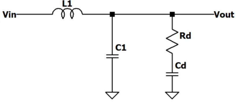
3.3
Output Stage Filter Design
The converter is controlled by a PWM signal which carries the envelope informa-tion. The voltage at the switching node between the transistors is an amplified version of the PWM control signal. Hence, the switching frequency needs to be filtered out by a low pass filter at the output of the converter. The filter should have a flat response in the passband covering the entire envelope bandwidth in order to prevent any distortion on the envelope information.
The filter design started with the conventional LC low pass filter shown in Fig. 3.5(a). Considering that the supply voltage is approximately 30 V, a filter that has 34 dB attenuation at 10 MHz, can reduce the ripple to approximately 700 mV. This ripple was accepted in order to widen the passband without further increasing the switching frequency.
A small valued inductor in the filter increases the RMS current and the power dissipation of the converter. Thus, a high valued inductor with low resistance needs to be used to prevent extra losses. On the other hand, the capacitor cannot be too low because of the impedance requirements of the RFPA drain. The capacitor bonds the quarter wavelength transmission line at the drain to the ground. If the capacitance is low, the quarter wavelength transmission line is not grounded for low frequencies. This situation may cause low frequency oscillations in the RFPA.
By considering these requirements, a low ESR 1.5 nF ceramic capacitor and a 8.2 µH power inductor with low resistance were used in the filter. The frequency response of the conventional LC filter is shown in Fig. 3.7. The resonance peaking
(a) Conventional Low Pass Filter (b) Filter with RC Damping Branch
Figure 3.5: Filter Schematics
arises from the underdamped characteristic of the filter. A big voltage oscillation occurs at this frequency since the LC circuit has a high output impedance at the resonance. In order to get a flat frequency response in the passband, the filter needs to be damped. For this purpose, a parallel damping method shown in Fig. 3.5(b) was applied to the filter. On the other hand, the resistor in the damping branch dissipates extra power because of the AC current components flowing through this circuit.
Figure 3.6: Low Pass Filter Topology
Transfer function of the filter given in Fig. 3.6 is as follows:
G(s) = Vout Vin
= RdCds + 1
RdCdL1C1s3+ L1(C1 + Cd)s2+ RdCds + 1
(3.8)
In [31], several optimization methods of this transfer function are presented. These methods provide different damping levels. The higher damping leads to
high Cd and higher power loss. In order to minimize the extra loss,
Butter-worth optimization results were used to design the damping branch. By apply-ing a1=a2=b2=1 to Eqs. 3.9, 3.10 and 3.11, the components are calculated as
Cd=4.5 nF and Rd=70 Ω. RdCd = (a1+ a2) ω0 (3.9) L1(C1+ Cd) = (a1a2+ b2) ω2 0 (3.10) RdCdL1C1 = a1b2 ω3 0 (3.11)
The effect of the RC damping branch is shown in Fig. 3.7. The resonance peaking was reduced from 12 dB to 3 dB by using this method. The resulting filter will be used the track the signals up to 1 MHz.
3.4
Envelope Amplifier Measurement
Efficiency performance of the converter including the driver losses is displayed in Fig. 3.8. The measurements were taken for 10 MHz and 20 MHz switching frequencies with 30 V input voltage and 80% duty cycle. Since the efficiency drop is significant with 20 MHz, switching frequency of 10 MHz was used in the design.
0.1 0.2 0.3 0.4 0.5 0.6 0.7 0.8 0.9 1
Output Current (A)
74 76 78 80 82 84 86 88 90 92 Converter Efficiency (%)
Figure 3.8: Measured Efficiency of the Envelope Amplifier for 10 MHz (Blue) and 20 MHz (Red)
Chapter 4
Design of the RF Power
Amplifier
4.1
Class AB Power Amplifier Design
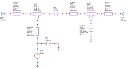
In this ET RFPA system, a class-AB type power amplifier was designed using 10 W CGH40010 RF Power GaN HEMT transistor from Cree. The matching circuits were designed for the 50 MHz band centered at 2.1 GHz. Large signal model of the transistor in AWR Microwave Studio was used in the simulations. The block diagram of the design is given in Fig. 4.1.
The algorithm followed in the design is given below.
• Determine and apply the bias condition
• Measure the input impedance and provide conjugate matching to the input • Perform load-pull analysis to find the optimum output impedance for high
power and efficiency
Figure 4.1: Power Amplifier Circuit
• Satisfy the stability conditions by using RC stability circuits at the input • Optimize the matching circuits for the required output power, efficiency,
stability and small signal S-parameters
For the class-AB design, the bias point was selected at VDD=28 V and
IDQ=200 mA. Then, the gate voltage was adjusted as −2.72 V for the selected
drain current. Under this bias condition, the input impedance was measured as in Fig. 4.2. For the load pull analysis, an ideal matching tool was used at the input to provide conjugate matching. The result of the load pull analysis is given in Fig. 4.3. As shown in the figure, 23+j8 Ω load impedance is considerably close to the maximum output power and maximum PAE.
In order to satisfy the input and output impedance requirements obtained by the simulations, the input and output matching circuits were designed with real components. The bias circuits were designed as shorted quarter wavelength transmission lines. In the matching circuits, transmission lines ended with shunt capacitors were preferred for easy tuning. In the input matching circuit, two RC circuits were included to satisfy unconditional stability. Both circuits were designed to establish resistive paths for the low frequencies that are inclined to oscillate.
0 1. 0 1. 0 -1 .0 10 .0 10.0 -1 0. 0 5. 0 5.0 -5 .0 2. 0 2. 0 -2 . 0 3. 0 3.0 -3 .0 4. 0 4.0 -4 .0 0. 2 0. 2 -0.2 0. 4 0 . 4 -0. 4 0. 6 0 . 6 -0 .6 0. 8 0 . 8 -0 .8 Swp Max 2200MHz Swp Min 2000MHz 2100 MHz r 2.48 Ohm x 4.2 Ohm S(1,1) Input_impedance
Figure 4.2: Input Impedance Analysis
After the final optimization, the input matching circuit given in Fig. 4.4 and the output matching circuit given in Fig. 4.5 were obtained. The layout of the PA circuit is displayed in Fig. 4.6. The circuit was fabricated on Rogers 4350 substrate material with 20 mil thickness together with the envelope amplifier as shown in Fig. 4.7.
0 1. 0 1. 0 -1 .0 10 .0 10.0 -1 0. 0 5. 0 5.0 -5 .0 2. 0 2. 0 -2 . 0 3. 0 3.0 -3 .0 4. 0 4.0 -4 .0 0. 2 0. 2 -0.2 0. 4 0 . 4 -0. 4 0. 6 0 . 6 -0 .6 0. 8 0 . 8 -0 .8 Swp Max 66 Swp Min 5 p18 p17 p16 p15 p14p13 p12 p11 p20 p19 p10 p9p8 p7 66 % r 23.4 Ohm x 8.3 Ohm PAE = 66 % iPower = 1 F1 = 2.1e+009 42 dBm r 23.4 Ohm x 8.3 Ohm PLoad = 42 dBm iPower = 1 F1 = 2.1e+009 PAE Pout p7: PAE = 56 % iPower = 1 F1 = 2.1e+009 p8: PAE = 58 % iPower = 1 F1 = 2.1e+009 p9: PAE = 60 % iPower = 1 F1 = 2.1e+009 p10: PAE = 62 % iPower = 1 F1 = 2.1e+009 p19: PAE = 64 % iPower = 1 F1 = 2.1e+009 p20: PAE = 66 % iPower = 1 F1 = 2.1e+009 p11: PLoad = 35 dBm iPower = 1 F1 = 2.1e+009 p12: PLoad = 36 dBm iPower = 1 F1 = 2.1e+009 p13: PLoad = 37 dBm iPower = 1 F1 = 2.1e+009 p14: PLoad = 38 dBm iPower = 1 F1 = 2.1e+009 p15: PLoad = 39 dBm iPower = 1 F1 = 2.1e+009 p16: PLoad = 40 dBm iPower = 1 F1 = 2.1e+009 p17: PLoad = 41 dBm iPower = 1 F1 = 2.1e+009 p18: PLoad = 42 dBm iPower = 1 F1 = 2.1e+009
Figure 4.3: Load Pull Simulation
MSUB Er=3.7 H=20 mil T=0.7 mil Rho=1 Tand=0.0035 ErNom=3.7 Name=SUB1 DCVS ID=V2 V=-2.72 V RES ID=R2 R=37 Ohm CAP ID=C6 C=10000 pF RES ID=R3 R=42 Ohm MTRACE2 ID=X1 W=42 mil L=150 mil BType=2 M=1 MSUB=SUB1 MTRACE2 ID=X2 W=42 mil L=50 mil BType=2 M=1 MSUB=SUB1 MTRACE2 ID=X3 W=80 mil L=100 mil BType=2 M=1 MSUB=SUB1 MTRACE2 ID=X4 W=12 mil L=870 mil BType=2 M=1 MSUB=SUB1 MTRACE2 ID=X5 W=42 mil L=290 mil BType=2 M=1 MSUB=SUB1 1 2 3 MTEE ID=TL1 W1=42 mil W2=42 mil W3=42 mil MSUB=SUB1 1 2 3 MTEE ID=TL2 W1=42 mil W2=42 mil W3=42 mil MSUB=SUB1 1 2 3 MTEE ID=TL3 W1=42 mil W2=42 mil W3=42 mil MSUB=SUB1 1 2 3 MTEE ID=TL4 W1=80 mil W2=42 mil W3=12 mil MSUB=SUB1 1 2 3 MTEE ID=TL5 W1=50 mil W2=50 mil W3=50 mil MSUB=SUB1 1 2 3 MTEE ID=TL6 W1=50 mil W2=50 mil W3=50 mil MSUB=SUB1 CAP ID=R1 C=100 pF MBENDA ID=TL7 W=42 mil ANG=90 Deg MSUB=SUB1 MBENDA ID=TL8 W=42 mil ANG=90 Deg MSUB=SUB1 MBENDA ID=TL9 W=42 mil ANG=90 Deg MSUB=SUB1 MBENDA ID=TL10 W=42 mil ANG=90 Deg MSUB=SUB1 MTRACE2 ID=X6 W=42 mil L=20 mil BType=2 M=1 MSUB=SUB1 MTRACE2 ID=X7 W=42 mil L=20 mil BType=2 M=1 MSUB=SUB1 MTRACE2 ID=X8 W=42 mil L=20 mil BType=2 M=1 MSUB=SUB1 MTRACE2 ID=X9 W=42 mil L=20 mil BType=2 M=1 MSUB=SUB1 MTRACE2 ID=X10 W=42 mil L=40 mil BType=2 M=1 MSUB=SUB1 CHIPCAP ID=C8 C=2.7 pF Q=7549.8 FQ=150 MHz FR=7447.2 MHz ALPH=-1 CHIPCAP ID=C12 C=2.2 pF Q=8370.2 FQ=150 MHz FR=8171.3 MHz ALPH=-1 CHIPCAP ID=C13 C=2 pF Q=8750.6 FQ=150 MHz FR=8531.9 MHz ALPH=-1 PORT P=1 Z=50 Ohm PORT P=2 Z=50 Ohm in_C1=2.59 in_L1=150 in_R2=37.1 in_C2=2.46 in_L3=49.9 in_R4=42.5 in_C4=2.13
CAP ID=C2 C=10000 pF DCVS ID=V2 V=28 V MTRACE2 ID=X5 W=42 mil L=314 mil BType=2 M=1 MSUB=SUB1 MTRACE2 ID=X1 W=42 mil L=200 mil BType=2 M=1 MSUB=SUB1 MTRACE2 ID=X2 W=42 mil L=829 mil BType=2 M=1 MSUB=SUB1 MSUB Er=3.7 H=20 mil T=0.7 mil Rho=1 Tand=0.0035 ErNom=3.7 Name=SUB1 1 2 3 MTEE ID=TL1 W1=80 mil W2=42 mil W3=42 mil MSUB=SUB1 1 2 3 MTEE ID=TL2 W1=42 mil W2=42 mil W3=42 mil MSUB=SUB1 MTRACE2 ID=X3 W=80 mil L=100 mil BType=2 M=1 MSUB=SUB1 CAP ID=C3 C=100 pF CHIPCAP ID=C5 C=1.98 pF Q=9168 FQ=150 MHz FR=8949.1 MHz ALPH=-1 PORT P=1 Z=50 Ohm PORT P=2 Z=50 Ohm out_C1=2.12 out_L1=314
Figure 4.5: Output Matching Circuit
4.2
Simulation Results
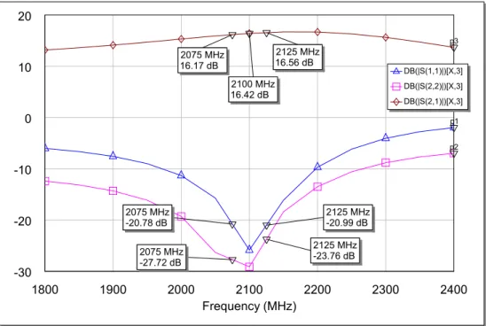
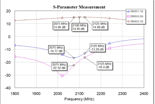
As the small signal S-parameter results given in Fig. 4.8 indicate, the input and output return losses are higher than 20 dB in the band. The small signal gain is 16.4±0.25 dB. 1800 1900 2000 2100 2200 2300 2400 Frequency (MHz) -30 -20 -10 0 10 20 p2 p3 p1 2075 MHz -27.72 dB 2075 MHz -20.78 dB 2125 MHz 16.56 dB 2075 MHz 16.17 dB 2100 MHz 16.42 dB 2125 MHz -23.76 dB 2125 MHz -20.99 dB DB(|S(1,1)|)[X,3] DB(|S(2,2)|)[X,3] DB(|S(2,1)|)[X,3] p1: Pwr = 24 dBm p3: Pwr = 24 dBm p2: Pwr = 24 dBm
Figure 4.8: S-Paratemer Simulation
As shown in Fig. 4.9, the stability factor K is higher than unity for all frequen-cies where the transistor has high gain. Since the drain voltage of the amplifier will be dynamically adjusted, the stability was checked for different supply volt-ages.
To check the large signal performance, output power and PAE are plotted over a range of input power. As displayed in Fig. 4.10, nearly 41 dBm output power with 65% PAE can be obtained with 30 dBm input power.
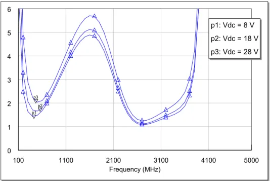
100 1100 2100 3100 4100 5000 Frequency (MHz) 0 1 2 3 4 5 6 p3 p2 p1 K() PA p1: Vdc = 8 V p2: Vdc = 18 V p3: Vdc = 28 V
Figure 4.9: K Factor Simulation
20 22 24 26 28 30 Input Power (dBm) 30 35 40 45 50 Ou tpu t Pow er ( dBm) 30 40 50 60 70 PAE ( %) p1 30 dBm 40.96 dBm 30 dBm 65.3 PAE(PORT_1,PORT_2)[11,X] (R) PA.AP_HB DB(PT(PORT_2))[11,X] (L, dBm) PA.AP_HB p1: Freq = 2100 MHz p2: Freq = 2100 MHz
4.3
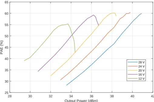
Measurement Results
After some tuning on the fabricated circuit, the results shown in Figs. 4.12 and 4.13 were obtained. The large signal measurements were repeated for different supply voltages. As expected, the power amplifier requires 28 V supply to get 41 dBm output power. However, the back off power levels can be obtained with lower supply voltages by maintaining the high efficiency. On the other hand, the gain drops with lower supply voltages. These measurement results will be used to do proper mapping between the input power and the required supply voltage.
28 30 32 34 36 38 40 42 Output Power (dBm) 25 30 35 40 45 50 55 60 65 PAE (%) 28 V 24 V 20 V 16 V 12 V
Figure 4.12: Output Power and PAE Measurement
18 20 22 24 26 28 30 32 Input Power (dBm) 2 4 6 8 10 12 14 16 Gain (dB) 28 V 24 V 20 V 16 V 12 V
Chapter 5
Slow Tracking and Supply Signal
Generation
5.1
Envelope Bandwidth Elimination
For high switching frequencies, switching losses become dominant and degrade the efficiency significantly. Therefore, the signal bandwidth that the converter can track is limited by the switching losses. In order to apply envelope tracking for the signals with wider bandwidth, slow tracking methods are used. Using these methods, a slew rate limited version of the envelope is tracked instead of tracking the exact envelope. On the other hand, slow tracking reduces the efficiency because, the bandwidth eliminated envelope does not keep the RFPA in compression region all the time. However, the efficiency degradation due to the slow tracking may not be so crucial since most of the envelope’s energy is concentrated at low frequencies.
In generating such a bandwidth eliminated envelope, there is an important restriction that needs to be taken into account. As given in Fig. 4.12, it is not possible to reach high RF power levels with low supply voltages. If the slow envelope is lower than the real envelope, a lower voltage than the minimum
required voltage is supplied to the RFPA yielding that the required RF power level cannot be obtained. Hence, the slow envelope must be higher than the real envelope at every time instance. Generating such an envelope is not possible by using a conventional causal low pass filter. In order to avoid missing any peak points, non-causal methods are used.
In this design, the envelope bandwidth is eliminated by using the algorithm described in [32] that is based on tracking the input signal with a predetermined maximum slew rate. The algorithm works based on the following rules:
• At each time n, the increase and decrease must be lower than the determined slew rate.
• At each time n, next N values must be known to see if there is a need for increase in order to catch the next peaks. The N is selected such that the original slew rate allows us to catch the peaks after N values.
Let E(n) be the real envelope signal, Es(n) be the slew rate limited version
and d is the maximum change between two adjacent points (i.e., the maximum slew rate = d× Sampling Rate), the mathematical expression of the algorithm can be written as given below.
y(n) = max
i=0,1,...,N(E(n + i) − i × d) (5.1)
Es(n) = max(y(n), Es(n − 1) − d) (5.2)
The original envelope and the slew rate limited versions are shown in Fig. 5.1 and Fig. 5.2.
In order to determine the appropriate slew rate limit for this application, the final supply signal corresponding the limited envelope was displayed in frequency domain. The cumulative distribution function of the frequency components were
5.5 5.55 5.6 5.65 5.7 5.75 5.8 5.85 5.9 5.95 Time (s) 10-4 16 18 20 22 24 26 Signal Envelope (dBm) Real Envelope
Slew Rate Limited Envelope
Figure 5.1: Real Envelope and Slew Rate Limited Version in Time Domain
examined. Since the envelope amplifier and the filter were designed to have a flat tracking response in 1 MHz band, the maximum slew rate was selected such that 90% of the frequency components resides at less than 1 MHz as shown in Fig. 5.3.
5.2
Supply Signal Generation
In this application, the supply signal is generated at the digital side in PWM for-mat. After the generation of the baseband signal, the envelope of the RF signal at the input of the power amplifier, is calculated in dBm format. The overall gain of the transmitter signal chain before the RFPA is required for this calculation. The envelope bandwidth elimination is applied after this stage. Then, the required supply signal is calculated based on the envelope of the RF signal at the input of the PA.
The RFPA measurement results in Figs, 4.12 and 4.13 were used for the proper mapping between the input power and the required supply.
Figure 5.2: Real Envelope and Slew Rate Limited Version in Frequency Spectrum
supply voltage. In order to maximize the overall efficiency, the mapping between the input power and the supply signal is done by interpolating these peak efficiency points.
• In Fig. 4.13, for each peak points, find the required input power to generate the corresponding output power with that supply voltage.
The look up table showing these values is given in Table 5.1. Table 5.1: Lookup Table of the Peak Efficiency Points
Supply Voltage Output Power Input Power
28 V 41 dBm 31 dBm
24 V 39.5 dBm 30 dBm
20 V 38 dBm 28 dBm
16 V 36 dBm 26.5 dBm
12 V 33 dBm 24 dBm
The discrete values in the look up table were put in a continuous form by using polynomial interpolation. The quadratic polynomial in Eqn. 5.3, was used
0 0.5 1 1.5 2 2.5 3 Frequency (MHz) 0 10 20 30 40 50 60 70 80 90 100 CDF % X 1.009 Y 89.9766
Figure 5.3: CDF of the Supply Signal
to generate the supply signal (V) as a function of the input power (dBm) of the RFPA. The discrete points and the interpolation are shown in Fig. 5.3.
y(x) = 0.12285x2− 4.5208x + 49.737 (5.3)
The RFPA gain significantly drops for lower supply voltages than 10 V. In order to prevent the nonlinearity because of the gain drop for lower supply voltages, a detroughing factor is applied. The envelope corresponding low supply voltages, is not tracked by applying a minimum voltage limit. In this application, the minimum supply was selected as 10 V. So, the supply signal changes between 10 V and 28 V.
Finally, the PWM signal is generated based on the calculated supply signal. As a simple method, the PWM signal is generated by comparing the supply signal with a saw tooth waveform. The sawtooth frequency determines the PWM period and switching frequency.
Chapter 6
Measurement
6.1
AM Signal Measurement
The test setup that was used in the measurements is given in Fig. 6.1. The baseband signal and its envelope are generated in Matlab. The required supply signal is calculated from the envelope, and envelope elimination is applied if necessary. Then, the supply signal is converted to a PWM signal and sent to the arbitrary waveform generator.
4/15/2020 Untitled Diagram.drawio
Keysight 33600A
Arbitrary Waveform Generator
Keysight N5182B
Vector Signal Generator
EA RFPA LPF DPA Mini Circuits ZVE-3W-83+ Agilent MSO9254A Oscilloscope Agilent N9030A Signal Analyzer Es(t) S(t) Modulated Signal S(t) & Envelope ES(t)
Generated in Matlab EA RFPA LPF DPA Es(t) S(t) Modulated Signal S(t) & Envelope ES(t) Generation RFOUT ET RFPA
The baseband signal that is uploaded to the vector signal generator, is modu-lated onto the carrier frequency of 2.1 GHz. Then, a driver amplifier is used to amplify the modulated signal to the required drive level.
0 5 10 15 20 25 30 35 40 Time ( s) 14 16 18 20 22 24 26 28 30 32 Input Power (dBm)
(a) Input Signal
0 5 10 15 20 25 30 35 Time ( s) 10 12 14 16 18 20 22 24 26 28 Supply Voltage(V) (b) Supply Voltage
Figure 6.2: Modulated Signal Envelope and Supply Voltage Generated for AM Measurement
The first measurement was taken by using an AM signal with unsuppressed carrier. The baseband signal contains two equal amplitude frequency components which are 100 KHz and 250 KHz. The modulated signal is shown in Fig. 6.2(a) has 6.2 dB PAPR. Since the envelope resides in the passband region of the envelope amplifier, the envelope bandwidth elimination algorithm is not required at this measurement. By using the mapping described in Eq. 5.3, the supply signal given in Fig. 6.2(b) is generated from the modulated signal envelope.
The modulated signal output and the supply voltage observed on the oscillo-scope are displayed in Fig. 6.3. The frequency spectrum of the output signal is also given in Fig. 6.4. The intermodulation components appear at 37 dB below the carrier frequency.
When the generated baseband and envelope signals are applied to the system, the overall efficiency appears to be 45% by considering the driver losses and envelope amplifier losses. The efficiency with the same baseband signal under 28 V constant supply, was measured to be 32%.
Table 6.1: Summary of the Efficiency Performance in AM Measurement
Average Output Power Power Dissipation Overall Efficiency
Constant Supply 3.1 W 9.7 W 32 %
Envelope Tracking 3.0 W 6.7 W 45 %
Figure 6.3: AM Signal (Yellow) and Supply Voltage Waveform (Green)
2099.4 2099.6 2099.8 2100 2100.2 2100.4 2100.6 Frequency (MHz) -45 -40 -35 -30 -25 -20 -15 -10 -5 0 Normalized Power (dB/Hz)
Figure 6.4: Measured Output Power Spectrum of ET RFPA by Using the AM Signal
6.2
LTE Signal Measurement
In the second measurement, 3 MHz and 5 MHz LTE signals with 12 dB and 13 dB PAPR were applied to the system. For both of the signals, the envelope bandwidth was reduced to 1 MHz by using the envelope elimination algorithm. The supply voltage and the modulated signal observed on the oscilloscope are displayed in Fig. 6.5.
Table 6.2 summarizes the efficiency performance of the ET RFPA by comparing to using a 28 V constant supply. In Fig. 6.6, the normalized output power spectrum of the ET RFPA is displayed for the 5 MHz signal. The adjacent channel leakage ratio (ACLR) is measured as 26 dBc.
Figure 6.5: LTE Signal (Yellow) and Supply Voltage Waveform (Green) Table 6.2: Summary of the Efficiency Performance in LTE Measurement
PAPR Average Output Power Power Dissipation Overall Efficiency
Constant Supply (3 MHz) 12 dB 0.81 W 6.2 W 13 %
Envelope Tracking (3 MHz) 12 dB 0.79 W 3.0 W 26 %
Constant Supply (5 MHz) 13 dB 0.65 W 5.9 W 11 %
2095 2096 2097 2098 2099 2100 2101 2102 2103 2104 2105 Frequency (MHz) -45 -40 -35 -30 -25 -20 -15 -10 -5 0 Normalized Power (dB/Hz)
Chapter 7
Conclusion
In this thesis, the aim was to design and fabricate an ET RFPA to improve the back-off efficiency in order to operate efficiently with high PAPR signals. A synchronous buck converter which is one of the most fundamental topologies was adopted in the envelope amplifier. In order to attain a converter with high slew-rate and efficiency, GaN switching transistors and a fast driver circuit were chosen. Design steps of the filter at the converter output and the class-AB power amplifier were mentioned. The resulting envelope amplifier has a bandwidth of 1 MHz with the switching frequency of 10 MHz. In order to improve the bandwidth that can be tracked by the ET RFPA, a slew-rate elimination technique was used. At the end, the performance of system was tested by applying time-varying envelope signals. The resulting ET RFPA has 26% overall efficiency with the LTE signal that has 3 MHz and 12 dB PAPR. The overall efficiency is 20% in the case of 5 MHz and 13 dB PAPR signal.
Since the modern communication systems use signals with high bandwidth to achieve high data rates, the envelope amplifier has strong requirements of slew-rate and efficiency. In a design with discrete components, the efficiently achievable switching frequency is limited because of the parasitic loss and delay components on the circuit. Due to the significant switching losses at higher fre-quencies, the switching frequency of the envelope amplifier could not be increased
above 10 MHz. Then, 1 MHz bandwidth was achieved by using the output filter of the converter to have an acceptable switching ripple.
The design of the filter has critical importance in the envelope amplifier per-formance. The underdamped characteristic of the conventional low pass filter at the output of the converter may cause significant resonance peaking that may cause distortion and even damage the switching devices. Therefore, an efficient and damped filter topology is required with carefully selected components.
The envelope bandwidth elimination method helped to track the signals with higher bandwidth. However, this techniques have considerable drawbacks. By decreasing the maximum allowable slew-rate of the algorithm, the efficiency im-provement of the ET system is decreases as expected. In addition to that, using the slow version of the envelope, causes a nonlinear memory effect that degrades the linearity. LTE measurement results confirm these expectations. The adjacent channel leakage ratio of the system (ACLR) is measured as 26 dBc in the 5 MHz LTE measurement.
In this design, the GaN transistors provided considerably high switching ef-ficiency that is not easy to achieve with silicon devices. For future work, the bandwidth of the envelope amplifier can be improved more by using a linear-assisted hybrid topology together with the GaN switching devices. Also, an integrated design may lead to achieve higher switching frequencies efficiently. With a high bandwidth envelope amplifier, tracking the exact envelope without using the bandwidth elimination may be possible. In this case, a better linear-ity is expected since the memory effect distortion is cancelled. In addition to that, digital predistortion techniques can be employed to improve the linearity. As given in [33, 34], nonlinear behavior of the ET systems can be modelled and compensated by applying predistortion on the input signal.
Bibliography
[1] P. Asbeck and Z. Popovic, “ET Comes of Age: Envelope Tracking for Higher-Efficiency Power Amplifiers,” IEEE Microwave Magazine, vol. 17, pp. 16–25, March. 2016.
[2] C. Ramella, A. Piacibello, R. Quaglia, V. Camarchia, and M. Pirola, “High Efficiency Power Amplifiers for Modern Mobile Communications: The Load-Modulation Approach,” Electronics, vol. 96, Nov. 2017.
[3] Z. Popovic, “Amping Up the PA for 5G: Efficient GaN Power Amplifiers with Dynamic Supplies,” IEEE Microwave Magazine, vol. 18, pp. 137–149, May. 2017.
[4] Z. Zhang, L. E. Larson, and P. M. Asbeck, Design of Linear RF Outphasing Power Amplifiers. Norwood, MA: Artech House, 1st ed., 2003.
[5] H. Chirex, “High Power Outphasing Modulation,” Proceedings of the Insti-tute of Radio Engineers, vol. 23, pp. 1370–1392, Nov. 1935.
[6] M. P. van der Heijden, M. Acar, J. S. Vromans, and D. A. Calvillo-Cortes, “A 19 W High-Efficiency Wide-band CMOS-GaN Class-E Chireix RF Out-phasing Power Amplifier,” in 2011 IEEE MTT-S International Microwave Symposium, pp. 1–4, 2011.
[7] M. J. Pelk, W. C. E. Neo, J. R. Gajadharsing, R. S. Pengelly, and L. C. N. de Vreede, “A High-Efficiency 100-W GaN Three-Way Doherty Amplifier for Base-Station Applications,” IEEE Transactions on Microwave Theory and Techniques, vol. 56, no. 7, pp. 1582–1591, 2008.
[8] B. Kim, J. Kim, I. Kim, and J. Cha, “The Doherty Power Amplifier,” IEE Microwave Magazine, pp. 42–50, Oct. 2006.
[9] N. Srirattana, A. Raghavan, D. Heo, P. E. Allen, and J. Laskar, “Analysis and Design of a High-Efficiency Multistage Doherty Power Amplifier for Wireless Communications,” IEEE Transactions on Microwave Theory and Techniques, vol. 53, pp. 852–860, Mar. 2005.
[10] R. Quaglia and S. C. Cripps, “A Load Modulated Balanced Amplifier for Telecom Applications,” IEEE Transactions on Microwave Theory and Tech-niques, vol. 66, pp. 1328–1338, Mar. 2018.
[11] D. J. Sheppard, J. Powell, and S. C. Cripps, “A Broadband Reconfigurable Load Modulated Balanced Amplifier (LMBA),” IEEE MTT-S International Microwave Symposium, pp. 947–949, 2017.
[12] D. Wang, D. F. Kimball, J. D. Popp, A. H. Yang, D. Y. Lie, P. M. Asbeck, and L. E. Larson, “An Improved Power-Added Efficiency 19-dBm Hybrid Envelope Elimination and Restoration Power Amplifier for 802.11g WLAN Applications,” IEEE Transactions on Microwave Theory and Techniques, vol. 54, pp. 4086–4099, Dec. 2006.
[13] F. H. Raab, B. E. Sigmon, R. G. Myers, and R. M. Jackson, “L-band trans-mitter using Kahn EER technique,” IEEE Transactions on Microwave The-ory and Techniques, vol. 46, no. 12, pp. 2220–2225, 1998.
[14] D. F. Kimball, J. Jeong, C. Hsia, P. Draxler, S. Lanfranco, W. Nagy, K. Linthicum, L. E. Larson, and P. M. Asbeck, “High-Efficiency Envelope-Tracking W-CDMA Base-Station Amplifier Using GaN HFETs,” IEEE Transactions on Microwave Theory and Techniques, vol. 54, no. 11, pp. 3848– 3856, 2006.
[15] D. Kim, D. Kang, J. Choi, J. Kim, Y. Cho, and K. Kim, “Optimization for Envelope Shaped Operation of Envelope Tracking Power Amplifier,” IEEE Transactions on Microwave Theory and Techniques, vol. 59, pp. 1787–1795, Jul. 2011.
[16] S. C. Cripps, RF Power Amplifiers for Wireless Communications. Norwood, MA: Artech House, 2nd ed., 2006.
[17] X. Cheng, Y. Xiong, X. Wang, P. Kumar, and Z. J. Shen, “Performance Analysis of Trench Power MOSFETs in Synchronous Buck Converter Appli-cations,” in APEC 07 - Twenty-Second Annual IEEE Applied Power Elec-tronics Conference and Exposition, pp. 332–338, 2007.
[18] L. R. Kahn, “Single-Sideband Transmission by Envelope Elimination and Restoration,” Proceedings of the IRE, vol. 40, no. 7, pp. 803–806, 1952. [19] B. D. Geller, F. T. Assal, R. K. Gupta, and P. K. Cline, “A technique for
the maintenance of FET power amplifier efficiency under backoff,” in IEEE MTT-S International Microwave Symposium Digest, pp. 949–952 vol.3, 1989. [20] A. A. M. Saleh and D. C. Cox, “Improving the Power-Added Efficiency of FET Amplifiers Operating with Varying-Envelope Signals,” IEEE Transac-tions on Microwave Theory and Techniques, vol. 31, no. 1, pp. 51–56, 1983. [21] J. Staudinger, B. Gilsdorf, D. Newman, G. Norris, G. Sadowniczak, R. Sher-man, and T. Quach, “High efficiency CDMA RF power amplifier using dy-namic envelope tracking technique,” in 2000 IEEE MTT-S International Mi-crowave Symposium Digest (Cat. No.00CH37017), vol. 2, pp. 873–876 vol.2, 2000.
[22] G. Hanington, Pin-Fan Chen, P. M. Asbeck, and L. E. Larson, “High-efficiency power amplifier using dynamic power-supply voltage for CDMA applications,” IEEE Transactions on Microwave Theory and Techniques, vol. 47, no. 8, pp. 1471–1476, 1999.
[23] M. Hassan, L. E. Larson, V. W. Leung, and P. M. Asbeck, “A Combined Series-Parallel Hybrid Envelope Amplifier for Envelope Tracking Mobile Ter-minal RF Power Amplifier Applications,” IEEE Journal of Solid-State Cir-cuits, vol. 47, no. 5, pp. 1185–1198, 2012.
[24] P. Mahmoudidaryan, D. Mandal, B. Bakkaloglu, and S. Kiaei, “Wideband Hybrid Envelope Tracking Modulator With Hysteretic-Controlled Three-Level Switching Converter and Slew-Rate Enhanced Linear Amplifier,” IEEE Journal of Solid-State Circuits, vol. 54, no. 12, pp. 3336–3347, 2019.
[25] J. Jeong, D. F. Kimball, M. Kwak, C. Hsia, P. Draxler, and P. M. Asbeck, “Wideband envelope tracking power amplifier with reduced bandwidth power supply waveform,” in 2009 IEEE MTT-S International Microwave Sympo-sium Digest, pp. 1381–1384, 2009.
[26] Y. Zhang, M. Rodr´ıguez, and D. Maksimovi´c, “Very High Frequency PWM Buck Converters Using Monolithic GaN Half-Bridge Power Stages With In-tegrated Gate Drivers,” IEEE Transactions on Power Electronics, vol. 31, no. 11, pp. 7926–7942, 2016.
[27] S. Schafer, M. Litchfield, A. Zai, Z. Popov´ıc, and C. Campbell, “X-band MMIC GaN power amplifiers designed for high-efficiency supply-modulated transmitters,” in 2013 IEEE MTT-S International Microwave Symposium Digest (MTT), pp. 1–3, 2013.
[28] A. Sepahvand, Y. Zhang, and D. Maksimovic, “High efficiency 20–400 MHz PWM converters using air-core inductors and monolithic power stages in a normally-off GaN process,” in 2016 IEEE Applied Power Electronics Con-ference and Exposition (APEC), pp. 580–586, 2016.
[29] C. Florian, T. Cappello, R. P. Paganelli, D. Niessen, and F. Filicori, “Enve-lope tracking of an rf high power amplifier with an 8-level digitally controlled gan-on-si supply modulator,” IEEE Transactions on Microwave Theory and Techniques, vol. 63, no. 8, pp. 2589–2602, 2015.
[30] Y. Xiong, Modeling and Analysis of Power Mosfets for High Frequency DC-DC Converters. PhD thesis, University of Central Florida, 2008.
[31] R. K¨unzi, “Passive Power Filters,” CERN Yellow Reports, 07 2016. 10.5170/CERN-2015-003.265.
[32] G. Montoro, E. Bertran, and J. Berenguer, “A Method for Real-time Gen-eration of Slew-rate Limited Envelopes in Envelope Tracking Transmitters,” 2010 IEEE International Microwave Workshop Series on RF Front-ends for Software Defined and Cognitive Radio Solutions (IMWS), pp. 1–4, Feb. 2010. [33] A. Zhu, P. J. Draxler, C. Hsia, T. J. Brazil, D. F. Kimball, and P. M. As-beck, “Digital Predistortion for Envelope-Tracking Power Amplifiers Using Decomposed Piecewise Volterra Series,” IEEE Transactions on Microwave Theory and Techniques, vol. 56, no. 10, pp. 2237–2247, 2008.
[34] G. Montoro, P. L. Gilabert, J. Berenguer, and E. Bertran, “Digital Predistor-tion of Envelope Tracking Amplifiers driven by slew-rate limited envelopes,” in 2011 IEEE MTT-S International Microwave Symposium, pp. 1–4, 2011.