and Application in Charge Trapping
Memory Grown by Single ALD Step
Nazek El-Atab
1, Farsad Chowdhury
1, Turkan Gamze Ulusoy
2,3, Amir Ghobadi
3,4,
Amin Nazirzadeh
3,4, Ali K. Okyay
2,3,4& Ammar Nayfeh
1Low-dimensional semiconductor nanostructures are of great interest in high performance
electronic and photonic devices. ZnO is considered to be a multifunctional material due to its unique properties with potential in various applications. In this work, 3-nm ZnO nanoislands are deposited by Atomic Layer Deposition (ALD) and the electronic properties are characterized by UV-Vis-NIR Spectrophotometer and X-ray Photoelectron Spectroscopy. The results show that the nanostructures show quantum confinement effects in 1D. Moreover, Metal-Oxide-Semiconductor Capacitor (MOSCAP) charge trapping memory devices with ZnO nanoislands charge storage layer are fabricated by a single ALD step and their performances are analyzed. The devices showed a large memory window at low operating voltages with excellent retention and endurance characteristics due to the additional oxygen vacancies in the nanoislands and the deep barrier for the trapped holes due to the reduction in ZnO electron affinity. The results show that the ZnO nanoislands are promising in future low power memory applications.
Nanoislands grown on solid surfaces constitute a nanostructured surface system with tunable electronic proper-ties and various applications in high performance electronic, optoelectronic and photonic devices. In photovolta-ics, nanoislands are shown to act as a light trapping scheme to enhance the solar cell’s efficiency1,2. A multimode
resistive switching is also demonstrated in single nanoisland systems3. Nanoislands can be deposited by different
techniques including chemical vapor deposition4, sputtering5, in addition to predefining the nucleation sites using
nanoindentation6, etc. Moreover, Zinc-Oxide (ZnO) has recently received considerable attention by industry and
research due to its excellent chemical and physical properties such as large bandgap, high exciton binding energy (60 meV), high transparency, high electron mobility, and high mechanical, chemical, and thermal stability at room temperature. These unique properties turn ZnO into a very attractive material with potential in numerous applications in electronics, optoelectronics, photocatalysis and laser devices7–13. ZnO is most commonly
depos-ited by either Atomic Layer Deposition (ALD) or physical vapor deposition such as sputtering. Within the past few years, ALD has gained world-wide attention for manufacturing conformal layers with thickness in the nano-meter range, particularly for microelectronic applications14–16. However, very recently, it has been shown that
the growth per cycle in ALD for the first 20 cycles can be less than a monolayer per cycle which promotes the growth of nanoislands described by a Volmer-Weber growth mechanism17. After multiple ALD cycles, the islands
start to coalesce and form a continuous film. However, in the ultra-thin-film regime, the ALD films are rough and not conformal to the initial substrate17. In the present study, ~3-nm ZnO nanoislands deposited by ALD
are demonstrated. Their physical and electronic properties are analyzed and their effect on the performance of Metal-Oxide-Semiconductor Capacitor (MOSCAP) charge trapping memory devices fabricated by single ALD step is investigated. In our previous works, we have demonstrated memory devices with different charge trap-ping layers such as graphene nanoplatelets18, InN nanoparticles19, ZnO nanoparticles20, Si-nanoparticles21–23, etc.
However, all of these nanomaterials have been deposited by spin/dip coating or drop-casting and therefore the memory was not grown by a single ALD step which would greatly reduce the possibility of contamination dur-ing the fabrication process. Moreover, we have previously shown memory devices with a continuous ZnO layer
1Institute Center for Microsystems – iMicro, EECS, Masdar Institute of Science and Technology Abu Dhabi, United
Arab Emirates. 2Institute of Materials Science and Nanotechnology, Bilkent University, 06800 Ankara, Turkey. 3UNAM-National Nanotechnology Research Center, Bilkent University, 06800 Ankara, Turkey. 4Department of
Electrical and Electronics Engineering, Bilkent University, 06800 Ankara, Turkey. Correspondence and requests for materials should be addressed to A.N. (email: [email protected])
received: 22 March 2016 Accepted: 15 November 2016 Published: 19 December 2016
deposited by ALD with 2-nm24 and 4-nm19 thicknesses. The achieved memory window was negligible even at
very large program/erase voltages (10/− 10 V) which show that the continuous ZnO layer deposited by ALD shows small charge trap states density unlike ALD deposited ZnO nanoislands.
Results
ZnO Nanoislands Deposition and Characterization.
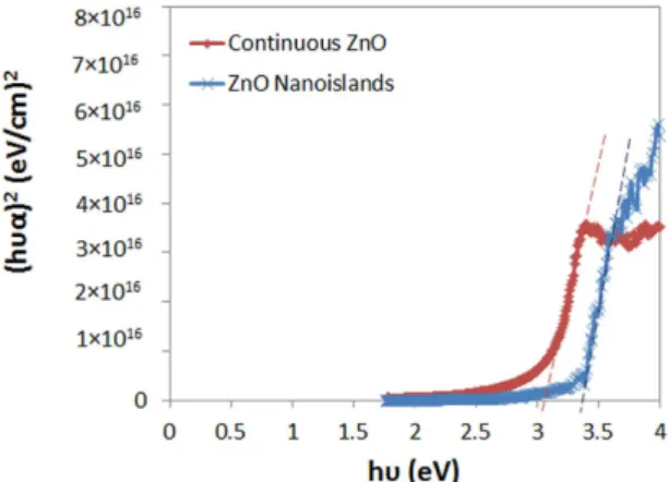
The ZnO islands are deposited by 20 ALD cycles at 180 °C on a lightly doped p-type Si substrate. The 2D and 3D Atomic Force Microscopy (AFM) topography plots (0.5 × 0.5 μ m) of the ZnO islands after performing tip de-convolution25 are depicted in Fig. 1a,b. Moreover,Fig. 1c shows the cross-sectional profile along the dashed line in Fig. 1a. The AFM images show that the nanois-lands are dispersed and separated from each other and have a width range from 8.5–30 nm (average ~20 nm) and an average thickness of ~3 nm. The transmittance and reflectance spectra are measured and the Kubelka-Munk function is used to extract the bandgap of the islands as shown in Fig. 226. The function consists of plotting (hυ α )2
vs. hυ where hυ is the photon energy and α is the absorption coefficient27–31. In fact,
Figure 1. ZnO nanoislands topography after performing AFM tip de-convolution. (a) 2D AFM image of nanoislands. (b) 3D AFM image of the nanoislands. (c) Cross-sectional profile of the islands across the dashed line shown in (a).
In the parabolic band structure, the absorption coefficient α and energy gap Eg of a direct-band gap material
are related through the known following equation32:
α υ =h A×(hυ −E )g 1/2 (1)
where hυ is the photon energy and A is a proportionality constant.
The absorption coefficient can be extracted from the transmittance and reflectance spectra using the following equation: α = − × − t ln (2) T R R T 1 1 s s bg bg
where t is the thickness of the semiconductor layer, Ts and Rs are the transmittance and reflectance measured
using the UV-Vis-NIR spectrophotometer on the sample, and Tbg and Rbg are the transmittance and reflectance of
the background (without the semiconductor layer).
Therefore, by measuring the needed reflectance and transmittance spectra, the absorption coefficient can be calculated and the bandgap can be therefore easily extracted using equation 1.
The same measurements are conducted on an 18-nm continuous ZnO layer. Figure 2 shows that the extracted bandgap of the continuous layer is 3.1 eV while this value for the islands increases to 3.35 eV due to quantum con-finement of charges in 1D. In fact, a thick-layer of semiconductor usually shows bulk properties of the material. As the dimension of the layer is reduced to be comparable to the Bohr radius of the excitons of the material, quan-tum confinement effects take place. If only one dimension of the material is reduced (such as thickness resulting in a thin layer), then quantum confinement effects in 1 dimension are expected. This means that the material is a 2D nanostructure (quantum well): the electrons/holes have 2 degrees of freedom in x and y, however, they are confined in the z-direction into specific discrete energy levels which depend on the size of the quantum well (i.e. thickness of the layer). The thickness of the islands is around 3-nm which is close to the Bohr radius of the excitons in ZnO (~2.3 nm) but the width is much larger (~20 nm). Therefore, quantum confinement of electrons along the thickness of the islands is expected.
However, Srikant el al. showed that the reported apparent bandgaps for ZnO of 3.1 eV and 3.2 eV in the liter-ature are due to the existence of a valence band-donor level transition at ~3.15 eV which can dominate the absorp-tion spectrum33. This value is close to the apparent bandgap reported in this work (3.1 eV) for the continuous
18-nm ZnO layer. In order to confirm the presence of defects levels in the deposited ZnO, X-ray photoelectron spectroscopy (XPS) measurements are conducted on the continuous and islands ZnO samples. First the energy difference between Zn2p and Si2p core levels ( ∆ECL) in the Si-ZnO (heterojunction) sample is measured and
found to be 923.46 eV as shown in Fig. 3a,b. On the other hand, (ECL−EVBM Si) , the energy difference of the core level to valance band maximum (VBM) for Si is determined as 98.85 eV from Fig. 4a. Whereas, this amount is found to be 1021.15 eV and 1019.23 eV for 3 nm and 18 nm thick ZnO layer, respectively. It should be noted that, as it can be implied from Fig. 4b,c, the value of EVBM shows a considerable change from 3.6 eV to 1.68 eV when we
move from continuous layer to nanoisland morphology. This is also in line with our assumption about emergence of quantum confinement effects for ultrathin ZnO layer. All obtained data are summarized in Table 1. Finally, the valence and conduction band offsets ∆(( EV) and (∆EC)) of Si/ZnO junction are calculated and summarized in Table 2. The results shown in Table 2 show that, due to quantum confinement, the electron affinity of the ZnO islands is reduced.
To explain this drastic shift in EVBM of nanoisland case, we need to analyze core-level spectrum of O 1 s for
ZnO layer. For this aim, this spectrum is deconvoluted to two main peaks located at ~ 530.7 eV corresponding to lattice oxygen (LO) and ~ 532.3 eV due to chemisorbed oxygen species at the lattice defect sites and oxygen
vacancies (VO)34. The existence of oxygen species such as –OH, –CO, adsorbed H2O and/or O2 on the surface
Figure 3. Core level spectra of (a) Zn 2p3/2 and (b) Si 2p3/2 recorded on Si-ZnO heterojunction. All peaks have been fitted to Voigt line shapes using a Shirley background.
generally produces a peak around 532.3 eV25,27. Looking at Fig. 5, we can see that the area under chemisorbed
oxygen peak is much higher for nanoisland case compared to continuous layer. Due to the fact that defect sites and grain boundaries are subjected to the chemisorption of the above ions, this confirms that the nanoisland ZnO layer contains much more oxygen defects compared to the continuous one. These oxygen-contained molecules are chemisorbed on the ZnO surface by capturing free electrons of the host material34–36. Therefore, in the vicinity
of the surface, these oxygen radicals decline the density of free carriers and deplete the surface electron states. This Figure 4. VB Spectra of (a) Si2p3/2 and Zn2p3/2 for (b) thick and (c) thin layers (VBM values are determined by extrapolating of leading edge to the base line).
Sample Region Binding Energy (eV)
Si VBM 0.52
ZnO (3 nm) VBM 1.68
ZnO (18 nm) VBM 3.6
Si/ZnO CL Si 2p3/2 99.37
CL Zn 2p3/2 1022.83
Table 1. Binding energies obtained by X-ray photoelectron spectroscopy measurements. Continuous ZnO (18-nm) ZnO islands (3-nm)
Eg 3.36 eV 3.604 eV
EC (Si) - EC (ZnO) 0.84 eV − 1.324 eV
EV (Si) - EV (ZnO) 3.08 eV 1.16 eV
Table 2. Conduction and valence band offsets between continuous and ZnO nanoislands on Si obtained by X-ray photoelectron spectroscopy measurements.
Figure 5. O 1 s spectra of ZnO layer for nano island and continuous films. Blue cure represents LO signal and
leads to formation of the space charge region which in turn leads to band bending near the surface region. Based on previous studies, Si (p-type)/ZnO (n-type) heterostructure have a surface band bending which is downward in Si side and upward in ZnO. Therefore, both quantum confinement effect and surface band bending cause this drastic change in the EVBM level of the nanoisland structure.
In principle there are four main types of defects on ZnO which can be classified as: oxygen vacancies (VO’s),
zinc vacancies (VZn’s) (surface defects), interstitials (Zni and Oi), and antisites which are mostly formed in the
bulk of material. The fact that which of these defects is dominant depends on the preparation method of the material under Zn reach conditions VO’s are the most favorable defects to form. This conclusion has been already confirmed by XPS measurement in which the O1s spectra show the existence of VO’s on the as prepared samples,
while there is no sign related to Zni in Zn2p spectra. These oxygen vacancies are of three types: Vo (neutral,
filled with 2 electrons, usually found at 0.4 eV from the valence band) VO+1 (charged, filled with one electron
or unoccupied and doubly degenerate, usually found at 1.04 and 2.56 eV from the valence band, respectively) and VO+2 (charged, unoccupied and doubly degenerate, usually found at around 3.1–3.2 eV from the valence
band)34,36,37. Figure 6 shows these estimated defect levels within the bandgap of our bulk ZnO37,38. For the
nano-islands, the bandgap is expected to be increased due to quantum confinement. The Kubelka-Munk plot showed a valence band-oxygen vacancy transition at around 3.35 eV since the bandgap of 2D ZnO nanostructures is reported to be around 3.62 eV39. Moreover, the XPS results show that the density of defects in the nanoislands is
much larger than in the bulk ZnO case. In addition, in order to estimate the bandgap of the ZnO nanoislands, a back-of-the-envelope method for 2D nanostructures is used by applying the following equation40:
= + − − π π ħ ħ E E m m 2 2 (3) g islands g bulk d e d h ( ) ( ) 2 2 2 2
where Eg(islands) and Eg(bulk) are the bandgaps of the ZnO islands and bulk ZnO, respectively, mh and me are the
effective masses of holes and electrons in ZnO respectively, (0.59m0 and 0.24m0, respectively)41, d is the thickness
of the islands (3-nm) and ħ is the reduced Plank’s constant. The calculated bandgap of the islands is 3.604 eV which is consistent with the reported bandgap of 2D- ZnO nanostructures (3.62 eV) in the literature39.
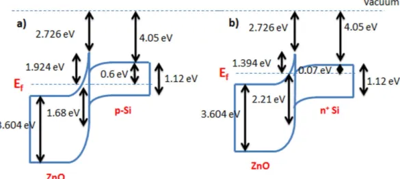
Based on the XPS measurements, the band diagrams of the ZnO islands/Si heterojunctions with p-type Si and highly doped n-type Si are shown in Fig. 7a,b, respectively. The figures show that the electron affinity of the ZnO is reduced to 2.726 eV which is an expected effect of quantum confinement. In addition, the band bending at the interface to align the Fermi level creates a barrier for trapped holes in the ZnO which helps in reducing the charge leakage probability as will be explained with more details in the following.
Memory Devices characterization.
The memory devices are fabricated on highly doped n+ type Si wafer(111) (Antimony doped, 15–20 mΩ -cm). Atomic layer deposited Al2O3 is used for both tunnel and blocking
oxides. ZnO nanoislands are used as the charge trapping layer. The 250-nm Al e-beam deposited contacts are patterned using a shadow mask. The deposition of the active layer of the memory in a single ALD step greatly reduces the contamination probability42. Figure 8a shows the cross-section illustration of the fabricated memory
devices. A reference memory without ZnO nanoislands is also fabricated. The devices are electrically character-ized by measuring the high-frequency (1 MHz) C-Vgate characteristics. A gate voltage of 6 V is first applied for 1 s
and the memory C-V is measured, followed by − 6 V for 1 s. A large memory window of 4 V is obtained as shown in Fig. 8b. Similar C-V measurements are conducted at different program/erase voltages. It is observed that the memory devices are being programmed by applying a negative gate voltage. Moreover, a very large threshold voltage (Vt) shift of 8.5 V is obtained at − 10/10 V program/erase voltage which proves that the ultra-thin ZnO
islands have a large density of charge trapping states while a very negligible shift is obtained in the reference cells as shown in Fig. 9.
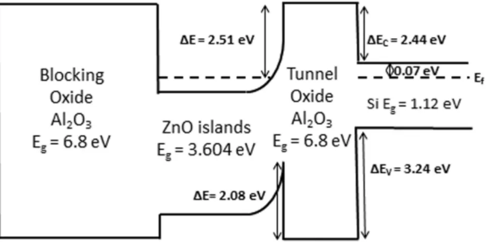
The energy band diagram of the memory cells are constructed as shown in Fig. 10 based on the XPS meas-urements and reported values of the band offsets and bandgaps of the different materials43–45. Therefore, during
the program operation when a negative gate voltage is applied, the electrons in VO and VO+ states gain enough
energy and get emitted to the channel while holes in the channel gain enough energy and tunnel through the tunnel oxide and get trapped within the deep quantum well formed by the valence band offsets. This will cause the programmed CV characteristic of the memory to shift to the left. During the erase operation, the electrons from the channel tunnel back into the trap states (oxygen vacancies + quantum well) within the ZnO bandgap while Figure 7. Energy band diagram of the ZnO islands/Si heterojunction. (a) With p-type Si. (b) With highly doped n-type Si.
Figure 8. Memory device with ZnO nanoislands. (a) Cross-sectional illustration of the memory. (b) High-frequency (1 MHz) C-V measurements of erased and programmed states of the memory devices.
Figure 9. Threshold voltage shift vs. program/erase voltage for the memory with nanoislands and reference memory.
holes in the quantum well tunnel back into the channel which will cause the CV characteristic of the memory to shift back to the right.
In addition, the retention characteristics of the memory cells is studied by first programming/erasing the memory at − 7/7 V and reading the memory state in time as shown in Fig. 11a. The retention characteristic extrapolated to 10 years shows a 3.85 V Vt shift where 14.4% of the initial charge is lost in 10 years. To explain the
good retention characteristic, we need to analyze the tunneling probability of the electrons from the channel back into the oxygen vacancies and the tunneling of the holes from the ZnO quantum well back into the channel with no applied gate voltage. First of all, for the electrons available in the channel to tunnel into the oxygen vacancies and quantum well, they must overcome a large barrier Δ EC of 2.44 eV (as shown in Fig. 10), therefore the
tun-neling/emission probability is very low especially when no electric field is applied (retention operation). Second, for the holes stored in the ZnO quantum well to leak back, they need to overcome a barrier Δ E of 2.08 eV caused by the reduction of the electron affinity of ZnO (as shown in the energy band diagram Fig. 10) which is also too large for holes which have a larger effective tunneling mass than electrons. Moreover, the endurance characteristic of the memory is analyzed by programming and erasing the cells at − 7/7 V up to 104 times while observing the
change in the Vt shift. As shown in Fig. 11b, after 104 cycles, a large memory window of 4 V is still measured which
means that ~11% of the initial charge is lost. This outstanding endurance characteristic shows that such memory structure is promising for future memory devices.
Discussion
The growth per cycle in ALD which is the amount of material deposited in an ALD reaction cycle, is a function of three parameters: the reactants, the reaction temperature, and the surface where the reactions occur46. A
con-stant growth per cycle has been a paradigm in ALD through decades47,48. Recently it has been realized that while
depositing new material, the ALD process changes the characteristics of the substrate, therefore the growth per cycle does not need to be constant49–52. Moreover, it has been shown that in the first ~20 ALD cycles (depending
on the material), 3D islands form in the so called Volmer-Weber growth mode53. In this growth mode, it has been
observed a generic stress evolution from compressive to tensile, then back to compressive stress as the film thick-ened. The tensile stress is attributed to the impingement and coalescence of growing islands: islands strain to close the gap between them and replace the free surfaces with a low energy grain boundary54,55. However, if the growth
process is interrupted at the islands stage, then the tensile stress will be relaxed and the mechanism depends sen-sitively on the process conditions, on whether the film is continuous or discontinuous, and on the film/substrate Figure 10. Energy band diagram of the memory with ZnO nanoislands showing the Fermi level.
Figure 11. Memory characteristics (a) Retention characteristic of the memory initially programmed/erased at − 7/7 V. (b) Endurance characteristic up to 104 cycles.
interfacial strength56. Some of the reported relaxation mechanisms include interfacial shear, selective relaxation
consistent with surface-diffusion-based mechanisms, and dislocations to name a few57–61. In our case, since the
memory showed a much larger memory window and therefore a larger charge trapping states density than in the case of continuous ZnO layer with almost the same thickness as reported in our previous work where a negligible Vt shift was obtained at 10/− 10 V program erase voltage19, then the tensile stress in the nanoislands is expected
to be relaxed through a mechanism that adds trap states in ZnO such as dislocations. In addition, oxygen vacan-cies are reported to relax the stress in ZnO62,63. Therefore, the observed larger density of oxygen vacancies in the
nanoislands than in the continuous ZnO could be due to the stress relaxation mechanism in the islands. As a matter of fact, the introduction of large densities of defects into semiconductors is needed in many applications. For example, the introduction of deep level defects moves the Fermi Level close to midgap and greatly increases the resistivity is desirable for photoconductors since it reduces the dark current. Another feature of high defect densities is an enhanced optical absorption in the spectral region below the edge for direct transitions due to the introduction of new states and the relaxation of selection rules for indirect transitions. A third advantage of the use of high defect density materials is the ease of fabrication of ohmic contacts. And for memory devices, the introduction of defects introduces additional trap states which enlarge the memory window.
Moreover, when programming the memory at higher negative voltages, the C-V curves shifts to the left indi-cating that holes are being stored and electrons are being removed. While at higher positive gate voltages, the C-V curves shift to the right indicating that electrons are being stored and holes are being removed. The reduction of the electron affinity of the ZnO due to quantum confinement increases the valence band offset between the charge trapping layer and surrounding tunnel and blocking oxides, and therefore, additional hole trap states are available. Additionally, the oxygen vacancies states contribute in trapping electrons. The charge trap states density can be calculated using the equation Δ N = Δ Vt × Cacc, where Δ Vt is the threshold voltage shift and Cacc is the
accumulation capacitance per unit area. Δ N is found to be 3.1 × 1013 cm−2.
In order to study the charge emission mechanism during the program/erase operations, the electric field across the tunnel oxide needs to be calculated using Gauss’s law. However, due to quantum confinement, the dielectric constant of the ZnO is expected to be lowered. Moreover, it is known that Fowler-Nordheim is the dominant tun-neling mechanism across Al2O3 when the electric field is > ~4.5 MV/cm64–66. Therefore, the electric field across
the tunnel oxide is calculated for different ZnO dielectric constant values. It is worth noting that the dielectric constant of bulk ZnO is around 10.8 while ZnO with quantum confinement effects in 3D (ZnO quantum dots) has a reported dielectric constant of around 3.767. Thus, the dielectric constant of the 2D ZnO islands is expected
to be in this range. Figure 12a shows the calculated electric field across the tunnel oxide when Vg = 6 V vs. the
ZnO dielectric constant, the figure shows that for dielectric constants above ~3.7, Eox > 4.5 MV/cm, therefore,
Fowler-Nordheim is expected to be the dominant charge emission mechanism in the memory device when the applied gate voltage is equal or greater than 6 V. In fact, F-N tunneling is the tunneling mechanism which requires the highest electric field across the tunnel oxide in order to create a triangular barrier through which charges can tunnel. For dielectric constants below 3.7, Eox < 4.5 MV/cm, and other emission mechanisms would be dominant
such as Phonon-Assisted Tunneling (PAT), Poole-Frenkel (PF), and Schottky emission (SE)68. Moreover, for a
dielectric constant of 3.7, the logarithm of the threshold voltage shift over the squared electric field across the tunnel oxide vs. the reciprocal of the electric field is plotted in Fig. 12b and the linear trend at Eox > 4.5 MV/cm
which corresponds to Vg = 6 V confirms that Fowler-Nordheim tunneling is the dominant emission mechanism.
In summary, 3-nm-thick ZnO nanoislands are deposited by ALD and characterized. The results show that due to quantum confinement in 1D, the bandgap of the nanoislands increases and the electron affinity is reduced. Moreover, memory devices with ZnO nanoislands charge trapping layer fabricated by a single ALD step are demon-strated. The measurements show that a large memory window of 4 V can be obtained at low operating voltages due to holes storage and electrons removal from the nanoislands. The increased charge trapping states density in the islands is due to additional defect states (oxygen vacancies) due to the tensile stress relaxation in the islands. Moreover, the reduction of the electron affinity of the ZnO created a deep barrier for the trapped holes in ZnO, improving the retention characteristic of the memory. The excellent retention and endurance characteristics of the memory indi-cate that ZnO nanoislands are promising in future nonvolatile charge trapping memory devices.
Figure 12. (a) Electric field across the tunnel oxide vs. the dielectric constant of the ZnO with an applied gate Vg = 6 V. (b) Natural logarithm of the threshold voltage shift over the squared electric field across the tunnel oxide
10 s, H2O dose: 100 ms, Ar purge: 10 s. Then, 10-nm Al2O3 blocking oxide is deposited at 300 °C and 80 mtorr. The
contacts are deposited using a Temescal e-beam deposition system at 3 × 10⁻⁶ torr and patterned using a shadow
mask. The electrical characterization of the devices is conducted using an Agilent B1505A semiconductor device analyzer connected to a Signatone probe station.
AFM Imaging.
For imaging, AC-in-Air imaging mode was used. Si based AFM cantilevers with Al reflective coating. The tips radii are ~9 nm according to the manufacturer specifications.References
1. Hu, Q., Wang, J., Zhao, Y. & Li, D. A light-trapping structure based on Bi2O3 nano-islands with highly crystallized sputtered silicon for thin-film solar cells. Optics express. 19(101), A20–A27 (2011).
2. Hu, Q., Wang, J., Cao, Y., Zhao, Y. & Li, D. Light-trapping enhancement based on Ga2O3 nano-islands coated glass substrate. Solar
Energy 86(3), 855–859 (2012).
3. Qi, J., Olmedo, M., Zheng, J. G. & Liu, J. Multimode resistive switching in single ZnO nanoisland system. Scientific reports 3 (2013). 4. Zaretski, A. V. et al. Metallic Nanoislands on Graphene as Highly Sensitive Transducers of Mechanical, Biological, and Optical
Signals. Nano letters 16(2), 1375–1380 (2016).
5. Sun, X. & Li, H. Gold nanoisland arrays by repeated deposition and post-deposition annealing for surface-enhanced Raman spectroscopy. Nanotechnology 24(35), 355706 (2013).
6. Alkhatib, A. & Nayfeh, A. A Complete Physical Germanium-on-Silicon Quantum Dot Self-Assembly Process. Scientific reports 3 (2013).
7. Bacaksiz, E. et al. The effect of zinc nitrate, zinc acetate and zinc chloride precursors on investigation of structural and optical properties of ZnO thin films. J. Alloy. Compd. 466, 447‒ 450 (2008).
8. Wang, J. et al. Synthesis and characterization of multipod, flower-like, and shuttle-like ZnO frameworks in ionic liquids. Mater. Lett.
59, 1405‒ 1408 (2005).
9. Özgür, Ü. et al. A comprehensive review of ZnO materials and devices. Journal of applied physics 98(4), 041301 (2005).
10. El-Atab, Nazek, et al. Diode behavior in ultra-thin low temperature ALD grown zinc-oxide on silicon. AIP Advances 3(10), 102119 (2013).
11. Ulusoy, T. G., Ghobadi, A. & Okyay, A. K. Surface Engineered Angstrom Thick ZnO-sheathed TiO2 Nanowires as Photoanode for Performance Enhanced Dye-sensitized Solar Cells. Journal of Materials Chemistry A 2, 16867–16876, doi: 10.1039/c4ta03445g (2014).
12. Ghobadi, A. et al. Enhanced Performance of Nanowire-Based All-TiO2 Solar Cells using Subnanometer-Thick Atomic Layer Deposited ZnO Embedded Layer. Electrochimica Acta 157, 23, doi: 10.1016/j.electacta.2015.01.079 (2015).
13. Battal, E. et al. Atomic Layer Deposited Zinc-Oxide as Tunable Uncooled Infrared Microbolometer Material. Physica Status Solidi A, doi: 10.1002/pssa.201431195 (2014).
14. Oruc, F. B. et al. Low Temperature Atomic Layer Deposited ZnO Photo Thin Film Transistors. Journal of Vacuum Science and
Technology A 33, 01A105, doi: 10.1116/1.4892939 (2015).
15. Leskelä, M. & Ritala, M. Atomic layer deposition (ALD): from precursors to thin film structures. Thin solid films. 409(1), 138–146 (2002).
16. Choy, K. L. Chemical vapour deposition of coatings. Progress in materials science. 48(2), 57–170 (2003).
17. Wu, M. K., Chen, M. J., Tsai, F. Y., Yang, J. R. & Shiojiri, M. Fabrication of ZnO nanopillars by atomic layer deposition. Materials
transactions. 51(2), 253–255 (2010).
18. Nayfeh, A., Okyay, A. K., El-Atab, N., Cimen, F. & Alkis, S. Transparent Graphene Nanoplatelets for Charge Storage in Memory Devices. Invited 226th ECS meeting 2014. no. 37, p. 1879–1879 (2014).
19. El-Atab, N. et al. Enhanced memory effect via quantum confinement in 16 nm InN nanoparticles embedded in ZnO charge trapping layer. Applied Physics Letters 104(25), 253106 (2014).
20. El-Atab, N. & Nayfeh, A. 1D vs. 3D quantum confinement in 1–5 nm ZnO nanoparticles agglomerations for application in charge trapping memory devices. Nanotechnology 27, 275205 (2016).
21. Nayfeh, A., Okyay, A. K., El-Atab, N., Ozcan, A. & Alkis, S. Low Power Zinc-Oxide Based Charge Trapping Memory with Embedded Silicon Nanoparticles. Invited, 226th ECS meeting 2014 no. 46, p. 2143–2143 (2014).
22. El-Atab, N. et al. Memory effect by charging of ultra-small 2-nm laser-synthesized solution processable Si-nanoparticles embedded in Si-Al2O3-SiO2 structure. Phys. Status Solidi A 212(8), 1751–1755 doi: 10.1002/pssa.201431802 (2015).
23. El-Atab, N., Turgut, B. B., Okyay, A. K., Nayfeh, M. & Nayfeh, A. Enhanced non-volatile memory characteristics with Quattro-layer graphene-nanoplatelets vs. 2.85-nm Si-nanoparticles with asymmetric Al2O3/HfO2 tunnel oxide. Nanoscale Res. Lett. 10(1), 248, doi: 10.1186/s11671-015-0957-5 (2015).
24. Oruç, F. B., Cimen, F., Rizk, A., Ghaffari, M., Nayfeh, A. & Okyay, A. K. Thin-film ZnO charge-trapping memory cell grown in a single ALD step. IEEE Electron Device Letters 33(12), 1714–1716 (2012).
25. MountainsMap
®
software by Digital Surf.26. El-Atab, N. et al. Growth of ~3-nm ZnO Nano-islands Using Atomic Layer Deposition. To be published and presented at 2016 IEEE
Nanotechnology Conference Sendai, Japan, August 22–25 (2016).
bottom-up approach to control defect density. Nanoscale. 6(17), 10224–10234 (2014).
37. Ulusoy, T. G., Ghobadi, A. & Okyay, A. K. Surface engineered angstrom thick ZnO-sheathed TiO2 nanowires as photoanodes for performance enhanced dye-sensitized solar cells. Journal of Materials Chemistry A. 2(40), 16867–16876 (2014).
38. Hu, J. & Pan, B. C. Electronic structures of defects in ZnO: hybrid density functional studies. The Journal of chemical physics 129(15), 154706 (2008).
39. Samanta, P. K. Characteristics of benzene assisted grown ZnO nanosheets. Science of Advanced Materials. 4(2), 219–226 (2012). 40. Klimov, V. I. (Ed.). Semiconductor and metal nanocrystals: synthesis and electronic and optical properties. CRC Press (2003). 41. Jagadish, C. & Pearton, S. J. (Eds). Zinc oxide bulk, thin films and nanostructures: processing, properties, and applications. Elsevier
(2011).
42. Oruc, F. B. et al. Thin Film ZnO Charge Trapping Memory Cell Grown in a Single ALD Step. IEEE Electon Device Letters 33, 1714–1716, doi: 10.1109/LED.2012.2219493 (2012).
43. Wilk, G. D., Wallace, R. M. & Anthony, J. M. High-κ gate dielectrics: Current status and materials properties considerations. Journal
of applied physics 89(10), 5243–5275 (2001).
44. Huang, M. L. et al. Energy-band parameters of atomic-layer-deposition Al2O3/InGaAs heterostructure. Applied physics letters 89(1), 012903 (2006).
45. Lu, H. L. et al. Band alignment and interfacial structure of ZnO/Si heterojunction with Al2O3 and HfO2 as interlayers. Applied
Physics Letters. 104(16), 161602 (2014).
46. Goodman, C. H. & Pessa, M. V. Atomic layer epitaxy. Journal of applied physics. 60(3), R65–R82 (1986).
47. Leskelä, M. & Ritala, M. Atomic layer deposition chemistry: recent developments and future challenges. Angewandte Chemie
International Edition. 42(45), 5548–5554 (2003).
48. Suntola, T. Atomic layer epitaxy. Materials Science Reports. 4(5), 261–312 (1989).
49. Puurunen, R. L. Growth per cycle in atomic layer deposition: a theoretical model. Chemical Vapor Deposition. 9(5), 249–257 (2003). 50. Satta, A. et al. Growth mechanism and continuity of atomic layer deposited TiN films on thermal SiO2. Journal of applied physics.
92(12), 7641–7646 (2002).
51. Puurunen, R. L. Analysis of hydroxyl group controlled atomic layer deposition of hafnium dioxide from hafnium tetrachloride and water. Journal of applied physics 95(9), 4777–4786 (2004).
52. Alam, M. A. & Green, M. L. Mathematical description of atomic layer deposition and its application to the nucleation and growth of HfO2 gate dielectric layers. Journal of applied physics. 94(5), 3403–3413 (2003).
53. Puurunen, R. L. & Vandervorst, W. Island growth as a growth mode in atomic layer deposition: A phenomenological model. Journal
of Applied Physics. 96(12), 7686–7695 (2004).
54. Nix, W. D. & Clemens, B. M. Crystallite coalescence: A mechanism for intrinsic tensile stresses in thin films. Journal of Materials
Research 14(08), 3467–3473 (1999).
55. Freund, L. B. & Chason, E. Model for stress generated upon contact of neighboring islands on the surface of a substrate. Journal of
Applied Physics. 89(9), 4866–4873 (2001).
56. Floro, J. A. et al. The dynamic competition between stress generation and relaxation mechanisms during coalescence of Volmer–Weber thin films. Journal of Applied Physics. 89(9), 4886–4897 (2001).
57. Floro, J. A. et al. Novel SiGe island coarsening kinetics: Ostwald ripening and elastic interactions. Physical review letters. 84(4), 701 (2000).
58. Family, F. & Meakin, P. Scaling of the droplet-size distribution in vapor-deposited thin films. Physical review letters. 61(4), 428 (1988).
59. Thouless, M. D. Effect of surface diffusion on the creep of thin films and sintered arrays of particles. Acta metallurgica et materialia.
41(4), 1057–1064 (1993).
60. Floro, J. A. et al. The dynamic competition between stress generation and relaxation mechanisms during coalescence of Volmer–Weber thin films. Journal of Applied Physics. 89(9), 4886–4897 (2001).
61. Kobrinsky, M. J. & Thompson, C. V. The thickness dependence of the flow stress of capped and uncapped polycrystalline Ag thin films. Applied physics letters. 73(17), 2429–2431 (1998).
62. Janotti, A. & Van de Walle, C. G. Native point defects in ZnO. Physical Review B. 76(16), 165202 (2007).
63. Conchon, F. et al. X-ray diffraction analysis of thermally-induced stress relaxation in ZnO films deposited by magnetron sputtering on (100) Si substrates. Thin Solid Films. 518(18), 5237–5241 (2010).
64. Groner, M. D., Elam, J. W., Fabreguette, F. H. & George, S. M. Electrical characterization of thin Al2O3 films grown by atomic layer deposition on silicon and various metal substrates. Thin Solid Films. 413(1), 186–197 (2002).
65. Shen, Y. D. et al. Excellent insulating behavior Al2O3 thin films grown by atomic layer deposition efficiently at room temperature.
Optoelectronic and advanced materials 6(5), 618–622 (2012).
66. Mahajan, A. M., Khairnar, A. G. & Thibeault, B. J. Electrical properties of MOS capacitors formed by PEALD grown Al2O3 on silicon. Semiconductors 48(4), 497–500 (2014).
67. Lin, K. F., Cheng, H. M., Hsu, H. C., Lin, L. J. & Hsieh, W. F. Band gap variation of size-controlled ZnO quantum dots synthesized by sol–gel method. Chemical Physics Letters 409(4), 208–211 (2005).
68. Ramesh, S., Dutta, S., Shankar, B. & Gopalan, S. Identification of current transport mechanism in Al2O3 thin films for memory applications. Applied Nanoscience 5(1), 115–123 (2015).
69. El-Atab, N. et al. Growth of ~3-nm ZnO Nano-islands Using Atomic Layer Deposition. Proceedings of the 16th IEEE International
institutional affiliations.
This work is licensed under a Creative Commons Attribution 4.0 International License. The images or other third party material in this article are included in the article’s Creative Commons license, unless indicated otherwise in the credit line; if the material is not included under the Creative Commons license, users will need to obtain permission from the license holder to reproduce the material. To view a copy of this license, visit http://creativecommons.org/licenses/by/4.0/