JW4A.2.pdf 2016 Imaging and Applied Optics Congress (3D, AO, AIO, COSI, DH, IS, LACSEA, MATH) © OSA 2016
Holograms Deep Inside Silicon
Ghaith Makey1, Onur Tokel1, Ahmet Turnali2, Ihor Pavlov1, Parviz Elahi1, ¨
Ozg ¨un Yavuz2and F. ¨Omer Ilday1,2
1Department of Physics, Bilkent University, 06800 Ankara, Turkey
2Department of Electrical and Electronics Engineering, Bilkent University, 06800 Ankara, Turkey
Abstract: Through the Nonlinear Laser Lithography method, we demonstrate the first computer generated holograms fabricated deep inside Silicon. Fourier and Fresnel holograms are fabricated buried inside Si wafers, and a generation algorithm is developed for hologram fabrication.
OCIS codes: 090.1760, 320.7130
Recently we have demonstrated the use of ultrafast lasers for creating extremely uniform structures over indefinite large surfaces with Nonlinear Laser lithography (NLL) [1]. The method relies on a novel physical mechanism which enables a plethora of laser created nanostructures on surfaces. Now with the extension of this mechanism to the third dimension, for the first time, we can create buried structures in silicon (Si) wafers without damaging the wafer surface [2–4]. The importance of this achievement is hard to overemphasize, since Si is the fundamental material in electronics, silicon photonics and solar cell technologies. Further, it has desired properties at the mid-infrared where functional optical elements are hard to fabricate. Here we demonstrate the first functional holograms created inside Si wafers. The phase delay along the fabricated micro-structures inside Si enables the translation of diffractive optics and holography lexicon to Si optics in unprecedented fashion. As a capability demonstration of the plethora of functional diffractive optical elements buried inside Si, here we present the first computer generated holograms; namely Fourier holograms to project high detailed 2D images, and Fresnel holograms to reconstruct 3D image projection.
a
b
c
d
e
Fig. 1 (a) The target image (source image). (b) Part of the generated hologram in Si. (c) Microscope image of portion of the fabricated hologram. (d) The reconstructed image by simulation (1st order only). (e) The optically reconstructed image (1st order only).
JW4A.2.pdf 2016 Imaging and Applied Optics Congress (3D, AO, AIO, COSI, DH, IS, LACSEA, MATH) © OSA 2016
In comparison to computer generated holograms (CGH) written on the surface of Si [5], which are based on amplitude modulation, Si embedded CGHs are based on phase modulation. The pixel based phase modulation enables implementing buried kinoforms (phase holograms), which also reduces the number of pixels in the hologram required to recreate an image. Moreover, the micro-structures inside Si exhibit high refractive index difference, in contrast to glass embedded CGHs, which increases the applicability of kinoforms inside Si compared to glass.
To design the kinoform binary holograms that can reconstruct both binary and gray-scale images at high fidelity, we developed and customized an algorithm. For Fourier holograms, we implemented a modified version of the adaptive-additive Iterative Fourier Transform Algorithm (IFTA) [6]. The modifications include customizing the spectral condition of adaptive-additive algorithm to yield binary phase holograms, and increasing the noise space of the algorithm to improve the quality of the reconstructed image. The result of the application of our algorithm is shown in Fig. 1, which shows the target image (the Mona Lisa, Fig 1a), part of the generated subsurface hologram (Fig. 1b), and simulation of the reconstructed image (Fig. 1d). The experimental result of the image generated by the hologram is given in Fig 1e. For the Fresnel hologram, we used the same algorithm to generate a stack of binary holograms, each able to create a slice of the intended 3D projection at a different distance. Then, we superimposed the generated holograms together and finally binarized the resulting hologram. The presented 3D projection of the Fresnel hologram was chosen to be rectangular twisted channel of 4 slices (Fig. 2).
Experimentally, the holograms were fabricated using a home-build 1.55 µm master oscillator power amplifier (MOPA) fiber laser. The silicon sample was processed on a three-axis motorized stage to enable precise positioning of the sample. The pixel size was chosen as 10 µm to keep the scalar wave equation valid, and also to reconstruct large images. A portion of the fabricated hologram is shown in Fig.1(c), where dark zones indicate processed areas. The holograms were fabricated up to 800 by 600 pixels in size.
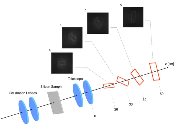
Fig. 2 The optical setup used to reconstruct Fresnel images of silicon subsurface holograms, and the optical constructed images of the 3D twisted channel (a,b,c,d).
JW4A.2.pdf 2016 Imaging and Applied Optics Congress (3D, AO, AIO, COSI, DH, IS, LACSEA, MATH) © OSA 2016
For Fourier holograms, the optical setup uses a 1 µm home-made fiber laser system, a digital camera after removing its IR filter, and focusing optics. Fig. 1(e) shows the final optical reconstruction of the image. As for Fresnel hologram, the reconstruction setup implemented the same laser, while the same camera was mounted on one-axis motorized stage to capture the different slices of the 3D projection. Fig. 2 shows both the optical reconstruction setup of Fresnel hologram and images of the optical reconstructed slices of the hologram’s 3D projection. Diffraction efficiency is defined as the power ratio of the diffraction’s first order to zeroth order, which is measured approximately as 200 % corresponding to a phase modulation depth of 0.73 π.
In conclusion, the first deeply buried silicon holograms are made possible by Nonlinear Laser Lithography. The algorithm for generating the embedded holograms was developed and optimized to reconstruct detailed 2D images via Fourier diffraction, and 3D projections by Fresnel diffraction. The presented holograms prove the ability to create a variety of diffractive optical elements inside Si, that can be used in wavefront correction and micro-optical applications. References
1. B. ¨Oktem, I. Pavlov, S. llday, H. Kalaycıo˘glu, A. Rybak, S. Yavas¸, M. Erdo˘gan, and F. ¨O. llday, “Nonlinear laser lithography for indefinitely large-area nanostructuring with femtosecond pulses,” Nature Photon. 7, 897 (2013). 2. O. Tokel, A. Turnali, I. Pavlov and F. ¨Omer Ilday, ”Laser writing deep inside silicon for 3D information
pro-cessing,” presented at CLEO/EU-EQEC, Munich, Germany, 21–25 June 2015.
3. O. Tokel, A. Turnali, I. Pavlov, F. ¨Omer Ilday , ”Physical model for subsurface silicon writing,” presented at CLEO-PR, Busan, Korea, 24–28 Aug 2015.
4. O. Tokel, A. Turnali, E. Ergecen, I. Pavlov, F. ¨Omer Ilday , ”3D Functional Elements Deep Inside Silicon with Nonlinear Laser Lithography,” presented at APS, Baltimore, Maryland, USA, 14–18 March 2016.
5. K. J. Waedegaard and P. Balling, ”High-resolution computer-generated reflection holograms with three-dimensional effects written directly on a silicon surface by a femtosecond laser,” Opt. Exp. 19, 3434 (2011) 6. ER. Dufresne, GC. Spalding, MT. Dearing, SA. Sheets and DG. Grier, ”Computer generated holographic optical