cations. To optimize the design parameters, the Sonnet (a method of moments (MoM) full-wave simulator) was used. Although the simulated results slightly disagree with the measured results due to the infinite-substrate presumption of the Sonnet simulator, the simulated results are still valuable and necessary. After the simu-lated optimum is obtained, the prototype is constructed by printing the patches on the 0.8-mm FR4 substrate. The reflection loss and radiation patterns are measured and discussed as follows.
The simulated and measured results of reflection loss are shown in Figure 2. The resonant frequencies are indeed located at the EGSM and DCS bands. The measured bandwidths (determined by 1:2.5 VSWR) are about 120 and 124 MHz at the EGSM and DCS bands, respectively. The bandwidths are almost large enough to meet the bandwidth requirements of the EGSM/DCS systems, and are much better than those obtained in [2– 4], especially at the EGSM band.
Measured radiation patterns are presented in Figures 3 and 4 for the resonant frequencies at the EGSM and DCS bands, respec-tively. For both resonant frequencies, good omnidirectional radi-ation is observed. The maximum antenna gains for both the co-polarization and cross-co-polarization patterns are estimated to be about 2.8 and 4.9 dBi across the EGSM and DCS bands, respec-tively.
4. CONCLUSION
A novel NMFGA design has been proposed. A dual-band NMFGA prototype has been shown as an example. It has been demonstrated that the resonant modes at the EGSM and DCS bands can be excited. As the measured and simulated results show, not only the radiation characteristics but also the impedance-matching band-widths are very attractive for EGSM/DCS dual-band applications. REFERENCES
1. K.L. Wong, Planar antennas for wireless communications, Wiley, Hoboken, 2003.
2. W.P. Dou and Y.W.M. Chia, Novel meandered planar inverted-F an-tenna for triple-frequency operation, Microwave Opt Technol Lett 27 (2000), 58 – 60.
3. F.R. Hsiao, H.T. Chen, T.W. Chiou, G.Y. Lee, and K.L. Wong, A dual band planar inverted-F patch antenna with a branch-line slit, Microwave Opt Technol Lett 32 (2002), 310 –312.
4. H.T. Chen, K.L. Wong, and T.W. Chiou, PIFA with a meandered and folded patch for the dual-band mobile phone application, IEEE Trans Antennas Propagat 51 (2003), 2468 –2471.
© 2004 Wiley Periodicals, Inc.
ANALYSIS OF FINITE ARRAYS OF
CIRCUMFERENTIALLY ORIENTED
PRINTED DIPOLES ON ELECTRICALLY
LARGE CYLINDERS
V. B. Ertu¨rk and Baris Gu¨ner
Department of Electrical and Electronics Engineering Bilkent University
TR-06800, Bilkent Ankara, Turkey
Received 17 January 2004
ABSTRACT: An efficient and accurate hybrid method of moments
(MoM)/Green’s function technique in the spatial domain is developed for the rigorous analysis of large, finite phased arrays of circumferen-tially oriented printed dipoles on electrically large, dielectric-coated, circular cylinders. Basic performance metrics (in the form of array cur-rent distribution, active reflection coefficient, far-field patterns, and so forth) of several arrays have been obtained and compared with similar printed arrays on grounded planar substrates. Certain discrepancies have been observed and discussed. © 2004 Wiley Periodicals, Inc.
Microwave Opt Technol Lett 42: 299 –304, 2004; Published online in Wiley InterScience (www.interscience.wiley.com). DOI 10.1002/mop. 20285
Key words: conformal phased array; method of moments; Green’s
function; coated cylinders
1. INTRODUCTION
A lot of potential applications in mobile communication and military systems require printed conformal arrays for aerodynamic reasons and/or to reduce the array’s radar cross section. However, available tools that can handle the rigorous analysis of microstrip structures on coated cylinders are usually restricted to small arrays or single antennas mounted on electrically small cylinders [1– 6]. When the number of elements in the array or the size of the cylinder (or both) increases, either some approximate models are used, where the mutual coupling between the array elements is ignored, or for antennas/arrays on electrically large cylinders, the shape of the host cylinder is considered only for the radiation patterns, and methods applicable to planar geometries are used in determining the array current distribution [5, 7–9]. Although this can be justified for the case of a single printed antenna, since it is a highly resonant structure [2, 7, 8], these methods produce inac-curate results for large arrays of printed antennas on large coated cylinders due to mutual coupling between the array elements through space and surface waves.
Recently, a hybrid the method of moments (MoM)/Green’s function technique in the spatial domain has been developed to perform a full-wave analysis of large phased arrays of axially oriented printed dipoles on electrically large, dielectric-coated, circular cylinders where all the mutual coupling effects are incor-porated [10]. It was shown in [10] that array-current distributions and basic performance metrics of relatively large arrays of axially oriented printed dipoles on cylindrical platforms significantly dif-fer from those of arrays of printed dipoles on grounded planar dielectric slabs [11].
In this paper, a study similar to [10] has been performed for the full-wave analysis of large, finite phased arrays of circumferen-tially oriented printed dipoles on electrically large, dielectric-coated, circular cylinders, where mutual coupling effects, array current distributions, and basic performance metrics of these arrays are compared to their planar counterparts, as well as arrays of axially oriented printed dipoles on the same cylinders. It has been Figure 4 Measured radiation patterns at 1810 MHz
shown that orientation of the array elements combined with the curvature effects significantly alters the basic performance metrics of arrays.
In section 2, the geometry and the formulation of the problem together with the high-frequency-based asymptotic Green’s func-tion representafunc-tions, used in this paper, are presented. In secfunc-tion 3, several numerical results involving the mutual coupling between two circumferentially oriented printed dipoles, array current dis-tributions for relatively large arrays, active reflection coefficients, and radiation patterns are presented both to assess the accuracy of this method and to demonstrate the curvature and array element orientation effects. An ejttime dependence is assumed and
sup-pressed throughout this paper. 2. FORMULATION
The geometry of a finite periodic array of (2N⫹ 1) ⫻ (2M ⫹ 1) identical, circumferentially oriented printed dipoles mounted on the dielectric-air interface of a dielectric-coated, perfectly conduct-ing, circular cylinder with radius a, coating thickness th (outer
radius d⫽ a ⫹ th), and relative permittivityr⬎ 1 is shown in
Figure 1(a). The cylinder is assumed to be infinite in the z-direction. For comparison purposes, the geometry of a finite, planar, periodic array of (2N⫹ 1) ⫻ (2M ⫹ 1) identical printed dipoles is also given in Figure 1(b). For both geometries, the dipoles are assumed to be center-fed with infinitesimal generators with impedance ZT, as depicted in Figure 1(c). Each dipole is
assumed to have a length L and width W [see Fig. 1(d)], and uniformly spaced from its neighbors by distances drl⫽ d⌬ and dz in the rl- (rl ⫽ d) and z-directions, respectively, for the
cylindrical array case, and dx and dyin the x- and y-directions,
respectively, for the planar array case.
Similar to [10] and [11], assumption of thin dipoles (W⬍⬍ L) requires only-directed currents. Then, an electric-field integral equation (EFIE) is formed by enforcing the boundary condition that the total Efield must vanish on the dipole surfaces. Using a single expansion mode per dipole and applying a Galerkin MoM approach, this EFIE is converted to the following set of linear equations [10, 11]:
共关Z兴 ⫹ 关ZT兴兲 䡠 I ⫽ V, (1)
where [Z]⫽ [Znm,pq] is the impedance matrix of the array with elements Znm,pq, which denotes the mutual impedance between
the nmthand pqth(⫺N ⱕ n, p ⱕ N, ⫺M ⱕ m, q ⱕ M) dipole,
given by Znm,pq⫽
冕
Spq dspq冕
Snm ds⬘nmfpq共rpq兲 G共rpq/r⬘nm兲 fnm共r⬘nm兲. (2)In Eq. (2), fnm(r⬘nm) and fpq(rpq) are the piecewise sinusoidal basis
and testing functions (one basis function per dipole) with rpqand r⬘nm being the position vectors of the pqth and nmth dipoles,
respectively, and G(rpq/r⬘nm) is the corresponding component
of the appropriate dyadic Green’s function for a dielectric-coated, electrically large circular cylinder [12–14]. In Eq. (1), [ZT] is the generator terminating impedance matrix (a diagonal matrix), and I ⫽ [Anm] is the unknown vector of expansion coefficients. Finally, V⫽ [Vpq ⫽ V0e⫺jk0sinid cos(i⫺p⌬)e⫺jk0 cosi
qdz] in Eq. (1)
denotes the excitation of the pqthdipole using a single expansion
mode per dipole with (i,i) being the scan direction of the main
beam. Note that V0 ⫽ 1 for uniform excitations in the present development similar to [10, 11].
The accuracy of the method comes from its rigor in which the mutual coupling between the dipoles through space and surface waves is incorporated. Although this calculation can be considered time consuming for large arrays, its efficiency comes from the fast computation of the appropriate dyadic Green’s function compo-nent G(rpq/r⬘nm), which is the kernel of the EFIE. Therefore,
three different spatial-domain representations of G(rpq/r⬘nm) are
used interchangeably, based on their computational efficiency and regions where they remain accurate. Furthermore, the three regions overlap (thus making the transition from one to another stable) and span the entire cylinder surface (thus making the mutual imped-ance calculations possible for arbitrary source and observation locations).
The first representation is a steepest descent path (SDP) repre-sentation of the dyadic Green’s function [12], which is based on the efficient numerical evaluation of a circumferentially propagat-ing (-propagating) series representation of the appropriate Green’s function along an SDP upon which the integrand decays most rapidly. This representation is valid away from the paraxial (nearly axial) region and cannot be used for self-impedance cal-culations. The second representation is the paraxial spatial-domain representation of the dyadic Green’s function [13], which comple-ments the SDP representation along the paraxial region. It is based on the periodicity of the-propagating series representation of the appropriate Green’s function in one of its variables. In this repre-sentation, G(rpq/r⬘nm) is written as the sum of the planar⫹
curvature correction terms [13], and making use of this periodicity, both terms are approximated by a Fourier series (FS), where the coefficients of these series expansions are obtained by simple Figure 1 (a) Geometry of a periodic array of (2N⫹ 1) ⫻ (2M ⫹ 1)
printed dipoles on a dielectric-coated, electrically large circular cylinder; (b) geometry of a periodic, planar array of (2N⫹ 1) ⫻ (2M ⫹ 1) printed dipoles; (c) dipole connected to an infinitesimal generator with a voltage
Vnmand a terminating impedance ZT; (d) representation of each dipole for
the MoM calculations. [Color figure can be viewed in the online issue, which is available at www.interscience.wiley.com]
numerical integration algorithms. Based on numerical experimen-tation, only the two leading terms of the expansion are necessary for the curvature correction term, whereas the planar term can exactly be expressed as a two term FS expansion. Finally, self-term (diagonal matrix elements of [Z]) evaluations are calculated using a highly efficient integral representation of the planar mi-crostrip dyadic Green’s function [14], assuming that electrically small surfaces (which are occupied by the self-term modes) can be considered to be locally flat for electrically large cylinders.
Once the mode currents are obtained from the solution of Eq. (1), several performance metrics, such as the active reflection coefficient at the nmthdipole, are given by
Rnm 共, 兲 ⫽ Zin nm共, 兲 ⫺ Z in mid共 ⫽ 90⬚, ⫽ 0⬚兲 Zin nm 共, 兲 ⫹ Zin mid *共 ⫽ 90⬚, ⫽ 0⬚兲, (3)
where the superscript mid stands for the middle element of the array, Zin
nm
⫽ Vnm/Anmis the input impedance of the nm thdipole.
The far-field radiation patterns of the array are investigated and compared with planar results.
3. NUMERICAL RESULTS AND DISCUSSION
Numerical results are presented (i) to demonstrate the efficiency and accuracy of this hybrid spatial domain MoM/Green’s function technique used for the rigorous analysis of a finite phased array of circumferentially oriented printed dipoles on coated circular cyl-inders, and (ii) to make a one-to-one comparison between the aforementioned arrays and arrays of printed dipoles on grounded planar slabs in order to show some discrepancies between their performance metrics, which are due to the curvature of the cylinder that alters the mutual coupling effects, especially in large arrays. To achieve these goals, the results obtained with the method presented in this paper are compared with the results of an eigen-function solution (based on the spectral domain MoM/Green’s function technique) for a coated cylinder with a ⫽ 30, th ⫽
0.060 and r ⫽ 3.25, as well as planar results with the same
thickness and relative dielectric constant. In all results, the size of each dipole is selected to be (L, W)⫽ (0.390, 0.010), and the periodicity of arrays is chosen to be 0.50 in the z- and rl-directions for circular arrays and x- and y-rl-directions for the planar arrays.
The first numerical result, shown in Figure 2, illustrates the mutual impedance Zmn,pq, as defined in Eq. (2), between two identical circumferentially oriented printed dipoles versus separa-tion s along the E- and H-planes, where the cylindrical spatial domain results are calculated for various cylinder radii and com-pared with planar results. Along the H-plane, mutual coupling between two identical -directed printed dipoles on a coated cylinder, which is dominated by the space waves, resembles to that of a planar case because, in general, waves along the paraxial region of a large cylinder behave similarly to waves excited on a planar grounded dielectric slab. Increasing the cylinder radius from 20to 50does not significantly affect the wave behavior along this plane, since the curvature effects are minimum. However, along the E-plane, where the curvature plays a major role, mutual coupling is significantly weaker than that of a planar case. As the radius of the cylinder is increased, coupling results approach to that of a planar case, as shown in Figure 2(b). As a result of this example, using planar approximations for a relatively large array of printed dipoles on large cylinders may yield inaccurate results due to the mutual coupling effects between the array elements along the E-plane.
Figure 3 illustrates the accuracy of this hybrid spatial-domain MoM/Green’s function technique, where both the array-current distribution and the active reflection coefficient magnitude 兩R兩 pertaining to a 3⫻ 3,-directed array of printed dipoles on a 3 cylinder are calculated and compared with those of both a refer-ence and planar solutions. Figure 3(a) shows the comparison of magnitudes of the induced current envelopes (that is,兩Anm兩) for the
middle row. To make a fair comparison between the cylindrical and planar results, the arrays are excited uniformly and elements of the voltage vectors are set to one for each pqthdipole. Similarly,
Figure 3(b) shows the comparison of兩R兩 versus the scan angle of the same array along the E- and H-planes, respectively. The兩R兩 values of all the arrays are computed at the center elements of the arrays, which are matched by a broadside scan. In all the figures, the results obtained with the cylindrical spatial domain method show an excellent agreement with the reference result (cylindrical spectral domain result) and exhibit a small disagreement with planar results. To generate the results in Figure 3(b), the cylindri-cal array is excited using the right hand side of Eq. (1). For the E-plane scan, the angleiis set to 90° andiis varied from 0° to
90°. Note that is defined from the z-axis for both geometries. Therefore, the E-plane result for the planar array is obtained by Figure 2 Magnitude of the mutual coupling Z12vs. separation s between
two printed identical dipoles along the (a) H- and (b) E-planes for grounded planar dielectric slab and coated cylinders withr⫽ 3.25, th⫽ 0.060,
and radii a⫽ 20(a⫽ 30, a⫽ 40, a⫽ 50, respectively). [Color
figure can be viewed in the online issue, which is available at www. interscience.wiley.com]
settingi ⫽ 0⬚ and varying i from 0° to 90° using a similar
excitation, as explained in [11]. On the other hand, for the H-plane scan, the cylindrical results are obtained by settingito 0° and
varyingifrom 90° to 0°, whereas for the planar resulti⫽ 90⬚
andivaries from 0° to 90°.
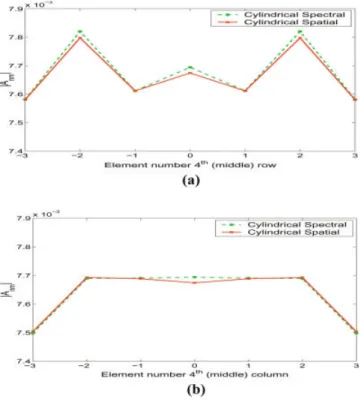
Figures 4(a) and 4(b) show the magnitudes of the induced current envelopes for the middle row and column of a 7⫻ 7 array for the broadside-scan case, where the cylindrical-spatial and spec-tral-domain results agree very well with each other. Small dis-agreements occur due to the accuracy problems of the spectral-domain results, since large separations between some elements in a relatively large array on an electrically large coated cylinder have an accuracy problem, due to the convergence of the Green’s function, in mutual impedance calculations when the spectral-domain technique is used. Therefore, for the rest of the numerical examples given in this paper, which are related to a larger array (11⫻ 11), only the spatial domain MoM/Green’s function tech-nique is used, since it is more accurate and more efficient (approx-imately 10 times) than its spectral-domain counterpart. Further-more, as the radius of the cylinder and/or the number of elements increase, (i) the difference in the fill time of the impedance matrix strongly favors the spatial domain technique, and (ii) the spectral-domain technique exhibits a convergence problem in the evalua-tion of mutual impedance between faraway elements.
In Figures 5(a)–5(d), induced current envelopes for the first and middle rows, (a) and (b), as well as the first and middle columns, (c) and (d), of a 11⫻ 11 array are compared with the planar results Figure 3 For a 3⫻ 3 array on a coated cylinder with r⫽ 3.25, th⫽
0.060, and a⫽ 30, comparison of the magnitude of (a) induced currents
兩Anm兩 for the middle (2
nd) row (E-plane) (n⫽ ⫺1:1 and m ⫽ 0) and (b)
reflection coefficients兩R兩 vs. scan angle in the E- and H-planes for the center element, obtained via cylindrical spatial, cylindrical spectral, and planar MoM. [Color figure can be viewed in the online issue, which is available at www.interscience.wiley.com]
Figure 4 For a 7⫻ 7 array, comparison of the magnitude of induced current兩Anm兩 obtained via cylindrical spatial and cylindrical spectral MoM
for the (a) middle (4th) row (E-plane) (n⫽ ⫺3:3 and m ⫽ 0); (b) middle
(4th) column (H-plane) (n⫽ 0 and m ⫽ ⫺3:3). Cylinder parameters are
the same as in Fig. 3. [Color figure can be viewed in the online issue, which is available at www.interscience.wiley.com]
Figure 5 For an 11⫻ 11 array, comparison of the magnitude of induced current兩Anm兩 obtained via cylindrical spatial and planar MoM for the (a)
first row (E-plane) (n ⫽ ⫺5:5 and m ⫽ ⫺5), (b) middle (6th) row
(E-plane) (n⫽ ⫺5:5 and m ⫽ 0), (c) first column (H-plane) (n ⫽ ⫺5 and
m⫽ ⫺5:5), (d) middle (6th) column (H-plane) (n⫽ 0 and m ⫽ ⫺5:5).
Cylinder parameters are the same as in Fig. 3. [Color figure can be viewed in the online issue, which is available at www.interscience.wiley.com]
to show that as the size of an array becomes larger, the array-current distributions for cylindrical and planar arrays differ from each other (which is a consequence of differences in mutual couplings). Once again, for a fair comparison, the arrays are excited uniformly and elements of the voltage vectors are set to one for each dipole.
The discrepancies in the array-current distribution between relatively large cylindrical and planar arrays lead to a difference in 兩R兩, particularly along the E-plane. This is illustrated in Figure 6, where兩R兩 versus the scan angles of 11 ⫻ 11 cylindrical and planar dipole arrays are depicted along the E- [Fig. 6(a)] and H-planes [Fig. 6(b)], respectively. The excitation of the arrays, for this example, is similar to that of the results presented in Figure 3(b), and the reflection coefficients of both arrays are computed at the center elements of the arrays which are matched at the broadside scan. However, because the size of the array is larger (11⫻ 11) in this example, the difference in the兩R兩 values between the cylin-drical and planar arrays is significant along the E-plane, when compared with the result of the 3⫻ 3 array depicted in Figure 3(b). It should be mentioned at this point that in a similar comparison, for an 11⫻ 11 axially oriented printed dipole array [10] (the same cylinder with the same parameters), scan blindness is observed at approximately 48°, where the planar reflection-coefficient magni-tude peaks. However, such an effect is not visible for the circum-ferentially oriented printed-dipole array. Similarly, when兩R兩 ver-sus element position along the E-plane for cylindrical and planar arrays are compared for various scan angles, as depicted in Figure 7, the differences in 兩R兩 curves are visible. Furthermore, scan blindness is not observed for the cylindrical array. However, for the 11 ⫻ 11 axially oriented printed dipole array (the same cylinder with the same parameters), a number of dipole ports have 兩R兩 values greater than unity as reported in [10]. Therefore, orien-tation of the array elements are also important, and when combined
with the curvature effects, the combination significantly alters some of the performance metrics of arrays.
Finally, the normalized far-field radiation pattern of this 11⫻ 11 phased array of printed dipoles is obtained and compared with that of a planar one for a 45° scan angle shown in Figure 8. Both arrays are scanned along the E-plane. Therefore, for the cylinder geometry,iis kept constant at 90° while the angle is scanned,
whereas for the planar array,iis kept at 0° and the angle is
scanned. It is observed that the pattern of a cylindrical printed-dipole array is close to that of a planar one along the main beam; Figure 6 Magnitude of the reflection coefficient兩R兩 vs. scan angle in the
(a) E-plane, (b) H-plane for the center element of both the cylindrical and planar geometries. Array and cylinder parameters are the same as in Fig. 5. [Color figure can be viewed in the online issue, which is available at www.interscience.wiley.com]
Figure 7 Magnitude of the reflection coefficient兩R兩 vs. element position for the (a) E-plane of the cylindrical geometry (n⫽ ⫺5:5 and m ⫽ 0), (b) E-plane of the planar geometry (n⫽ ⫺5:5 and m ⫽ 0) for various scan angles. Array and cylinder parameters are the same as in Fig. 5. [Color figure can be viewed in the online issue, which is available at www. interscience.wiley.com]
Figure 8 Far-field pattern of printed dipole arrays on both the cylinder and planar substrates phased to radiate a beam maximum in the 45° direction. Array and cylinder parameters are the same as in Fig. 5. [Color figure can be viewed in the online issue, which is available at www. interscience.wiley.com]
however, away from the main lobe, the shape of the pattern changes significantly. This is expected due to the curvature effects of the cylinder. Furthermore, since both arrays are fed uniformly and no special beamforming techniques are applied, high sidelobes occur for the cylindrical array due to the fact that some of the element patterns have their peaks at angles other than the intended main-beam direction.
4. CONCLUSION
A hybrid MoM/Green’s function technique has been used as a full-wave solver in order to investigate large, finite phased arrays of circumferentially oriented printed dipoles on electrically large, dielectric-coated, circular cylinders. Numerical examples involv-ing mutual couplinvolv-ing effects, array-current distributions, and basic performance metrics of several arrays were presented and com-pared with similar printed arrays on grounded dielectric slabs and axially oriented printed dipole arrays on the same coated cylinder. It has been observed that the orientation of the array elements combined with the curvature effects significantly alters the basic performance metrics of the arrays.
REFERENCES
1. A. Nakatini, N.G. Alexopoulus, N.K. Uzunoglu, and P.L.E. Uslenghi, Accurate Green’s function computation for printed circuit antennas on cylindrical antennas, Electromagn 6 (1986), 243–254.
2. K.M. Luk, K.F. Lee, and J.S. Dahele, Analysis of cylindrical-rectan-gular patch antenna, IEEE Trans Antennas Propagat 37 (1989), 143– 147.
3. W.Y. Tam, A.K.Y. Lai and K.M. Luk, Mutual coupling between cylindrical-rectangular microstrip antennas, IEEE Trans Antennas Propagat 43 (1995), 897– 899.
4. A. Dreher and M. Thiel, Dyadic Green’s function of multilayer cylin-drical closed and sector structures for waveguide, microstrip-antenna, and network analysis, IEEE Trans Microwave Theory Tech 50 (2002) 2576 –2579.
5. I. Jayakumar, R. Garg, B.K. Sarap, and B. Lal, A conformal cylindrical microstrip array for producing omnidirectional radiation pattern, IEEE Trans Antennas Propagat 34 (1986), 1258 –1261.
6. K.-L. Wong, Design of nonplanar microstrip antennas and transmis-sion lines, Wiley, New York, 1999.
7. Y. Liu, Y. Wang, and R. Yang, A cylindrical spiral patch array, IEEE Trans Antennas Propagat 49 (2001), 196 –199.
8. J.-M. Jin, J.A. Berrie, R. Kipp, and S.-W. Lee, Calculation of radiation patterns of microstrip antennas on cylindrical bodies of arbitrary cross section, IEEE Trans Antennas Propagat 45 (1997), 126 –132. 9. D.H. Werner, R.J. Allard, R.A. Martin, and R. Mittra, A reciprocity
approach for calculating radiation patterns of arbitrarily shaped mi-crostrip antennas mounted on circularly cylindrical platforms, IEEE Trans Antennas Propagat 51 (2003), 730 –738.
10. V.B. Ertu¨rk, K.W. Lee, and R.G. Rojas, Analysis of finite arrays of axially directed printed dipoles on electrically large cylinders, IEEE Trans Antennas Propagat (to appear).
11. D.M. Pozar, Analysis of finite phased arrays of printed dipoles, IEEE Trans Antennas Propagat 33 (1985), 1045–1053.
12. V.B. Ertu¨rk and R.G. Rojas, Efficient computation of surface fields excited on a dielectric coated circular cylinder, IEEE Trans Antennas Propagat 48 (2000), 1507–1516.
13. V.B. Ertu¨rk and R.G. Rojas, Paraxial space-domain formulation for surface fields on dielectric coated circular cylinder, IEEE Trans An-tennas Propagat 50 (2002), 1577–1587.
14. S. Barkeshli, P.H. Pathak, and M. Marin, An asymptotic closed-form microstrip surface Green’s function for the efficient moment method analysis of mutual coupling in microstrip antennas, IEEE Trans An-tennas Propagat 38 (1990), 1374 –1383.
© 2004 Wiley Periodicals, Inc.
FAST ANALYSIS OF INTERCONNECT
RESPONSE ILLUMINATED BY AN
EXTERNAL ELECTROMAGNETIC FIELD
USING G-FDTD
Hong-Fang Jin,1,2Er-Ping Li,1Sheng Wang,1Le-Wei Li,2and
Wei Liang Yuan1
1Institute of High Performance Computing
Science Park Road #01-01 The Capricorn Singapore 117528
2Faculty of Engineering
National University of Singapore 10 Kent Ridge Crescent Singapore 119260
Received 6 February 2004
ABSTRACT: A modified finite-difference time-domain (FDTD) method,
called generalized total-field/scattered-field (G-TF/SF) FDTD, is applied to compute the interconnect response on an infinite dielectric substrate illuminated by an external electromagnetic field. This method is also extended form 2D to 3D. The current distributions on the strips ob-tained by using the 3D G-FDTD method are presented and are in good agreement with the results computed via the method of moments (MoM). The simulation results indicate that this method is efficient and accurate for the modeling of an infinite scatterer problem with a compact FDTD grid. © 2004 Wiley Periodicals, Inc. Microwave Opt
Technol Lett 42: 304 –307, 2004; Published online in Wiley Inter-Science (www.interscience.wiley.com). DOI 10.1002/mop.20286 Key words: finite-difference time-domain; interconnect; infinite
scat-terer
1. INTRODUCTION
Numerical modeling of EMI/EMC problems has become increas-ingly popular over the past few years, due to the availability of commercial EM modeling software and the drive to reduce the time spent on product development. Historically, the emission problem has had priority over the immunity problem and most of the focus on EMI modeling has been on radiated emissions. However, with the increase of circuit density in electronic devices as well as tighter regulation imposed by the new European EMI requirements in consumer markets, immunity of electronic systems is becoming increasingly critical in the design phase in order to ensure proper functioning under realistic conditions. As a conse-quence, accurate and cost-effective EMI solutions are expected.
Analysis of voltages and currents induced at the ends of the interconnect, where sensitive semiconductor components may be connected, is one of the main EMI concerns for assessment of the immunity of the PCB exposed to external electromagnetic radia-tion [1]. Most analyses of scattering from such structures have been performed in the frequency domain using a variety of nu-merical algorithms. However, with the dramatic advances in com-puter speed and memory capabilities, the FDTD method has be-come one of the leading tools for the analysis of electromagnetic propagation and scattering [2] due to its simplicity and exceptional effectiveness in modeling complex structures and media, espe-cially its time-domain characteristics. TF/SF formulation resulted from attempts to realize a plane-wave source that avoids the difficulties caused by using either hard sources or the initial-condition approach in modeling scattering problems. But in this formulation, the scatterer is confined within the TF/SF boundary, and if an infinite scatterer is involved, a very large scatterer is required to be modeled in FDTD grid. So it is not efficient for an