Integrated piezoresistive sensors for atomic force-guided scanning Hall
probe microscopy
A. J. Brook, S. J. Bending, J. Pinto, A. Oral, D. Ritchie et al.
Citation: Appl. Phys. Lett. 82, 3538 (2003); doi: 10.1063/1.1576914 View online: http://dx.doi.org/10.1063/1.1576914
View Table of Contents: http://apl.aip.org/resource/1/APPLAB/v82/i20
Published by the American Institute of Physics.
Additional information on Appl. Phys. Lett.
Journal Homepage: http://apl.aip.org/Journal Information: http://apl.aip.org/about/about_the_journal
Top downloads: http://apl.aip.org/features/most_downloaded
Information for Authors: http://apl.aip.org/authors
Integrated piezoresistive sensors for atomic force-guided scanning Hall
probe microscopy
A. J. Brook, S. J. Bending,a)and J. Pinto
Department of Physics, University of Bath, Bath, BA2 7AY United Kingdom
A. Oral
Department of Physics, Bilkent University, 06533 Ankara, Turkey
D. Ritchie and H. Beere
Cavendish Laboratory, Cambridge University, Cambridge, CB3 OHE United Kingdom
M. Henini
Department of Physics, University of Nottingham, Nottingham, NG7 2RD United Kingdom
A. Springthorpe
Nortel Networks Optical Components Inc., 3500 Carling Avenue, Ottawa, Ontario K2H 8E9, Canada
共Received 21 October 2002; accepted 31 March 2003兲
We report the development of an advanced sensor for atomic force-guided scanning Hall probe microscopy whereby both a high mobility heterostructure Hall effect magnetic sensor and an n-Al0.4Ga0.6As piezoresistive displacement sensor have been integrated in a single III–V
semiconductor cantilever. This allows simple operation in high-vacuum/variable-temperature environments and enables very high magnetic and topographic resolution to be achieved simultaneously. Scans of magnetic induction and topography of a number of samples are presented to illustrate the sensor performance at 300 and 77 K. © 2003 American Institute of Physics.
关DOI: 10.1063/1.1576914兴
The demonstration of p-Si atomic force microscopy
共AFM兲 cantilevers with piezoresistive detection1represented
a major milestone in the field of scanning probe microscopy as it allowed variable temperature atomic-resolution topo-graphic imaging without the need for optical sensing ele-ments with precise alignment criteria. There is much to be gained by the extension of piezoresistive detection to III–V semiconductor cantilevers since it would allow one to exploit the direct band gaps and high carrier mobilities in these ma-terials. In particular scanning tunneling microscope 共STM兲-guided scanning Hall probe microscopy共SHPM兲,2,3which is noninvasive and yields quantitative low-noise magnetic im-ages, could be extended to nonconducting or electrically un-connected samples. While the use of GaAs as a piezoresis-tive material has been limited by its low piezoresispiezoresis-tive coefficient,4 the Al content of n-AlxGa1⫺xAs alloys can be
tailored to give large piezoresistive coefficients.5 We have recently shown that high sensitivity piezoresistive detection can be achieved using a cantilever with an n-Al0.4Ga0.6As
layer as the piezoresistive sensing element.6Since our sensor is composed exclusively of AlxGa1⫺xAs alloy layers, which
can be grown with almost perfect epitaxy, it allows us to realize an integrated low-noise Hall probe in a high-mobility Al0.3Ga0.7As/GaAs two-dimensional electron gas 共2DEG兲
grown at the surface of the cantilever.
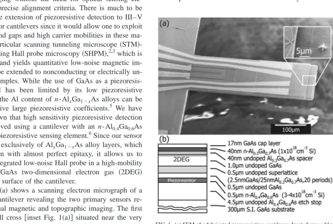
Figure 1共a兲 shows a scanning electron micrograph of a completed cantilever revealing the two primary sensors re-quired for dual magnetic and topographic imaging. The first sensor, a Hall cross 关inset Fig. 1共a兲兴 situated near the very
end of the cantilever, is electrically contacted via the four gold leads at either side of the cantilever. The piezoresistor is placed at the base of the cantilever where bending stresses are at a maximum. In addition a sharp (⬍100 nm diameter兲 AFM tip has been micromachined at the very end of the
a兲Electronic mail: [email protected]
FIG. 1.共a兲 SEM of a fabricated piezoresistive cantilever. Inset shows a blow up of the Hall probe and pyramidal AFM tip.共b兲 Epilayer structure for our integrated cantilever.
APPLIED PHYSICS LETTERS VOLUME 82, NUMBER 20 19 MAY 2003
3538
0003-6951/2003/82(20)/3538/3/$20.00 © 2003 American Institute of Physics
sensor, close to the Hall probe. The entire cantilever has been fabricated from a single GaAs/AlGaAs epilayer structure
关sketched in Fig. 1共b兲兴, grown by molecular beam epitaxy at
590 °C. From top to bottom the stack comprises a modula-tion doped n-Al0.3Ga0.7As/GaAs structure forming a 2DEG
⬃100 nm from the surface which is separated from the
n-Al0.4Ga0.6As piezoresistive layer by an electrical isolation
region composed of two undoped GaAs layers and an Al0.3Ga0.7As/GaAs superlattice. The micromachining steps
developed to realize the cantilever are reported elsewhere.6 The performance of the cantilever as an AFM sensor can be estimated from its geometry and material properties. For the rectangular cantilever shown in Fig. 1共a兲 the spring con-stant is well described by
k⫽Ewt
3
4L3 , 共1兲
where t is the thickness, w is the width, L is the length of the cantilever, and E is the Young’s modulus in the关011兴 direc-tion (E⫽12.2⫻1010Pa).7 The fractional resistance change
is given by
⌬R
R ⫽
3LEt关1⫺l/共2L兲兴共1⫺tr/t兲
2L2 ⌬z, 共2兲
where ⌬z is the deflection of the cantilever tip, tr is the thickness of the piezoresistor, andL is the longitudinal pi-ezoresistive coefficient. Using our known cantilever dimen-sions (L⫽400m, w⫽150m, t⫽6m, l⫽60m, and tr⫽0.5m) and piezoresistive coefficient (L⫽1.35
⫻10⫺9 Pa⫺1in n-Al
0.4Ga0.6As at 300 K兲6,8we calculate that
k⬵15 N/m and ⌬R/(R⌬z)⫽8.0⫻10⫺7 Å⫺1. The figure-of-merit of AFM sensor performance is the minimum detectable deflection 共MDD兲 whose fundamental limit is set by the Johnson noise (Vn⫽冑4kBTR⌬ f ) from the piezoresistor and the three identical resistors in the Wheatstone bridge into which it is incorporated. We estimate a MDD of 0.02 Å/冑Hz at 300 K for a typical piezoresistor with resistance 25 k⍀.
The performance of the Hall probe is also determined by its dimensions and the Johnson noise limit. The x – y resolu-tion of the sensor shown in Fig. 1共a兲 is limited to ⬃1m by the optical lithographic processing, although submicron probes could easily be realized by electron-beam lithography. The Johnson noise-limited minimum detectable field is given by Bmin⫽冑4kBTR⌬ f /IHRH where R is the series resistance of the voltage leads, IH is the Hall current and the RH Hall coefficient. For a 1 m Hall cross, with typical values of R
⫽80 k⍀, RH⫽3000 ⍀/T, and IH⫽4A at 300 K, a MDF of 3⫻10⫺6 T/冑Hz is estimated.
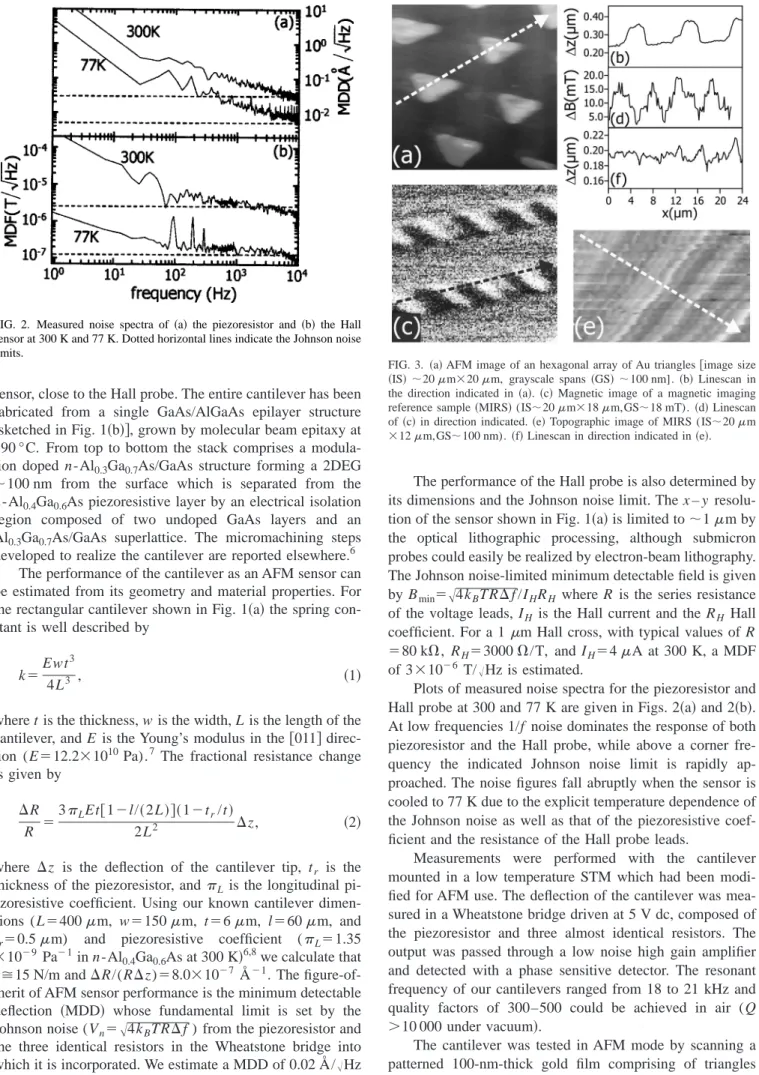
Plots of measured noise spectra for the piezoresistor and Hall probe at 300 and 77 K are given in Figs. 2共a兲 and 2共b兲. At low frequencies 1/f noise dominates the response of both piezoresistor and the Hall probe, while above a corner fre-quency the indicated Johnson noise limit is rapidly ap-proached. The noise figures fall abruptly when the sensor is cooled to 77 K due to the explicit temperature dependence of the Johnson noise as well as that of the piezoresistive coef-ficient and the resistance of the Hall probe leads.
Measurements were performed with the cantilever mounted in a low temperature STM which had been modi-fied for AFM use. The deflection of the cantilever was mea-sured in a Wheatstone bridge driven at 5 V dc, composed of the piezoresistor and three almost identical resistors. The output was passed through a low noise high gain amplifier and detected with a phase sensitive detector. The resonant frequency of our cantilevers ranged from 18 to 21 kHz and quality factors of 300–500 could be achieved in air (Q
⬎10 000 under vacuum兲.
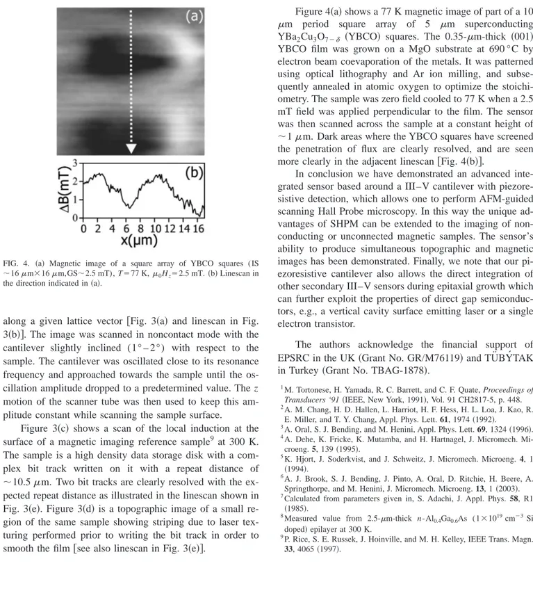
The cantilever was tested in AFM mode by scanning a patterned 100-nm-thick gold film comprising of triangles
共side length 5 m兲 in a hexagonal array with 10 m period
FIG. 2. Measured noise spectra of共a兲 the piezoresistor and 共b兲 the Hall sensor at 300 K and 77 K. Dotted horizontal lines indicate the Johnson noise limits.
FIG. 3. 共a兲 AFM image of an hexagonal array of Au triangles 关image size 共IS兲 ⬃20m⫻20m, grayscale spans共GS兲 ⬃100 nm]. 共b兲 Linescan in the direction indicated in 共a兲. 共c兲 Magnetic image of a magnetic imaging reference sample共MIRS兲 (IS⬃20m⫻18m,GS⬃18 mT). 共d兲 Linescan of共c兲 in direction indicated. 共e兲 Topographic image of MIRS (IS⬃20m ⫻12m,GS⬃100 nm). 共f兲 Linescan in direction indicated in 共e兲.
3539
Appl. Phys. Lett., Vol. 82, No. 20, 19 May 2003 Brooket al.
along a given lattice vector 关Fig. 3共a兲 and linescan in Fig. 3共b兲兴. The image was scanned in noncontact mode with the cantilever slightly inclined (1° – 2°) with respect to the sample. The cantilever was oscillated close to its resonance frequency and approached towards the sample until the os-cillation amplitude dropped to a predetermined value. The z motion of the scanner tube was then used to keep this am-plitude constant while scanning the sample surface.
Figure 3共c兲 shows a scan of the local induction at the surface of a magnetic imaging reference sample9at 300 K. The sample is a high density data storage disk with a com-plex bit track written on it with a repeat distance of
⬃10.5m. Two bit tracks are clearly resolved with the ex-pected repeat distance as illustrated in the linescan shown in Fig. 3共e兲. Figure 3共d兲 is a topographic image of a small re-gion of the same sample showing striping due to laser tex-turing performed prior to writing the bit track in order to smooth the film 关see also linescan in Fig. 3共e兲兴.
Figure 4共a兲 shows a 77 K magnetic image of part of a 10
m period square array of 5 m superconducting YBa2Cu3O7⫺␦ 共YBCO兲 squares. The 0.35-m-thick 共001兲
YBCO film was grown on a MgO substrate at 690 °C by electron beam coevaporation of the metals. It was patterned using optical lithography and Ar ion milling, and subse-quently annealed in atomic oxygen to optimize the stoichi-ometry. The sample was zero field cooled to 77 K when a 2.5 mT field was applied perpendicular to the film. The sensor was then scanned across the sample at a constant height of
⬃1m. Dark areas where the YBCO squares have screened the penetration of flux are clearly resolved, and are seen more clearly in the adjacent linescan 关Fig. 4共b兲兴.
In conclusion we have demonstrated an advanced inte-grated sensor based around a III–V cantilever with piezore-sistive detection, which allows one to perform AFM-guided scanning Hall Probe microscopy. In this way the unique ad-vantages of SHPM can be extended to the imaging of non-conducting or unconnected magnetic samples. The sensor’s ability to produce simultaneous topographic and magnetic images has been demonstrated. Finally, we note that our pi-ezoresistive cantilever also allows the direct integration of other secondary III–V sensors during epitaxial growth which can further exploit the properties of direct gap semiconduc-tors, e.g., a vertical cavity surface emitting laser or a single electron transistor.
The authors acknowledge the financial support of EPSRC in the UK 共Grant No. GR/M76119兲 and TU¨BY´TAK in Turkey 共Grant No. TBAG-1878兲.
1M. Tortonese, H. Yamada, R. C. Barrett, and C. F. Quate, Proceedings of
Transducers ‘91共IEEE, New York, 1991兲, Vol. 91 CH2817-5, p. 448.
2
A. M. Chang, H. D. Hallen, L. Harriot, H. F. Hess, H. L. Loa, J. Kao, R. E. Miller, and T. Y. Chang, Appl. Phys. Lett. 61, 1974共1992兲.
3A. Oral, S. J. Bending, and M. Henini, Appl. Phys. Lett. 69, 1324共1996兲. 4A. Dehe, K. Fricke, K. Mutamba, and H. Hartnagel, J. Micromech.
Mi-croeng. 5, 139共1995兲.
5K. Hjort, J. Soderkvist, and J. Schweitz, J. Micromech. Microeng. 4, 1
共1994兲.
6A. J. Brook, S. J. Bending, J. Pinto, A. Oral, D. Ritchie, H. Beere, A.
Springthorpe, and M. Henini, J. Micromech. Microeng. 13, 1共2003兲.
7
Calculated from parameters given in, S. Adachi, J. Appl. Phys. 58, R1 共1985兲.
8Measured value from 2.5-m-thick n-Al
0.4Ga0.6As (1⫻1019cm⫺3Si
doped兲 epilayer at 300 K.
9P. Rice, S. E. Russek, J. Hoinville, and M. H. Kelley, IEEE Trans. Magn.
33, 4065共1997兲. FIG. 4. 共a兲 Magnetic image of a square array of YBCO squares (IS
⬃16m⫻16m,GS⬃2.5 mT), T⫽77 K,0Hz⫽2.5 mT. 共b兲 Linescan in
the direction indicated in共a兲.
3540 Appl. Phys. Lett., Vol. 82, No. 20, 19 May 2003 Brooket al.