Journal of Physics: Conference Series
Negative refraction and focusing of
electromagnetic waves by photonic crystals
To cite this article: Irfan Bulu et al 2006 J. Phys.: Conf. Ser. 36 33
View the article online for updates and enhancements.
Related content
Frequency bands of negative refraction infinite one-dimensional photonic crystals
Chen Yuan-Yuan, Huang Zhao-Ming, Shi Jie-Long et al.
-Imaging by photonic crystal without negative refraction
Y Fang
-Imaging by Photonic Crystal Using Reflection and NegativeRefraction
Fang Yun-Tuan and Sun Hai-Jin
-Recent citations
Effective refractive index of the photonic crystal deduced from the oscillation model of the membrane
Ting-Hang Pei and Yang-Tung Huang
-Disorders influences on the focusing effect of all-dielectric photonic crystal slab superlens
Xiaoyong Hu et al
-Negative refraction in 2D photonic crystal super-lattice: towards devices in the IR and visible ranges
A. Frenkel et al
Negative refraction and focusing of electromagnetic
waves by photonic crystals
Irfan Bulu, Humeyra Caglayan, and Ekmel Ozbay
Department of Physics and Nanotechnology Research Center, Bilkent University, Ankara, Turkey
E-mail: [email protected]
Abstract. In this work, we study the negative refraction and focusing effect by a
metallodielectric photonic crystal. We show that by using a metallodielectric photonic crystal it is possible to obtain negative refraction for large incidence angles. In addition, our experimental and theoretical work reveal that the metallodielectric photonic crystal can be used as a flat-lens.
1. Metallodielectric Photonic Crystal
Since the pioneering works of Yablonovitch [1] and John [2] photonic crystals have attracted a great deal of interest. One of the major reasons for this interest is the rich dispersion relations of the photonic crystals. Dispersion properties of photonic crystals provide various means to control the propagation of electromagnetic (EM) waves. In this sense many applications such as waveguides [3, 4, 5], wavelength division multiplexing (WDM) [6, 7, 8, 9], highly directional antennas [10, 11] have been proposed and demonstrated.
Photonic crystals dramatically modify the dispersion properties of electromagnetic waves. An interesting phenomenon arising from the dispersion relation of photonic crystals is the so called negative refraction effect [12, 13, 14, 15, 16, 17]. This effect is observed for frequency ranges at which the wave vector of the incident waves and the group velocity of the transmitted waves fell into the opposite sides of the interface normal. As a result, for such frequency ranges photonic crystal behaves as if the index of refraction is negative.
In order to make use of the negative refraction effect in certain applications such as focusing of electromagnetic waves, one usually requires negative indices of refraction over a wide range of angles. To obtain negative indices of refraction over a wide range of angles is still a major challenge for photonic crystal based structures, especially for metallic photonic crystals. Due to the very large dielectric constants of metals (especially in microwave region), the bands that exhibit negative refraction for metallic photonic crystals occur at higher frequencies when compared to the dielectric photonic crystals with the same lattice parameters. As a result, it is difficult to obtain negative refraction of electromagnetic waves for large incidence angles by using metallic photonic crystals. In this work, we showed that by adding a periodic dielectric perturbation to the metallic photonic crystal, one can increase the range of angles at which negative indices of refraction are observed.
The metallodielectric photonic crystal that we used in our experiments and calculations is a square lattice of metallic and dielectric rods. The basis of the crystal consists of a metallic and a dielectric rod placed along the diagonal of the square unit cell (inset of Fig. 1). Cylindrical
33 © 2006 IOP Publishing Ltd
alumina rods with a radius of 1.55 mm are used for the dielectric rods and in the frequency range of interest the dielectric constant of alumina is 9.61. Metallic rods have a radius of 1.5 mm.
b)
0.0 0.2 0.4 0.6 0.8 Frequency ( ω a/2 π c) Γ Χ Μ Γ 0.0 0.2 0.4 0.6 0.8 Frequency ( ω a/2 π c) Γ Χ Μ Γ 0.2 0.4 0.6 0.8 1.0 1.2 Frequency ( ω a/2 π c) Γ Χ Μ Γ 0.2 0.4 0.6 0.8 1.0 1.2 Frequency ( ω a/2 π c) Γ Χ Μ Γa)
c)d)
Figure 1. The first 3 TM polarized bands for (a) the metallic photonic crystal (b) the metallodielectric photonic crystal (c) the unperturbed dielectric photonic crystal (d) the perturbed dielectric photonic crystal.
One can envision the metallodielectric photonic crystal, especially in the microwave region, as a metallic photonic crystal with a periodic dielectric perturbation [18, 19]. It is expected that an attractive perturbation, which corresponds to a positive dielectric constant, will result in lowering of bands. The computed band structures (for TM polarization: electric field is parallel to the axis of rods) for a metallic photonic crystal and a metallodielectric photonic crystal with the same lattice parameters are shown in Figs. 1(a), (b), and (c), respectively. We considered TM-polarized EM waves in our calculations and experiments. Figure 1(a) and (b) shows that the band structure of the metallodielectric photonic crystal is shifted to lower frequencies when compared to the metallic photonic crystal with the same lattice parameters. We have also computed the band structure of a dielectric photonic crystal and a perturbed dielectric photonic crystal. The perturbed dielectric photonic crystal has the same lattice constant of the dielectric photonic crystal and includes an additional dielectric rod in the unit cell. The results of our calculations are shown in Figs. 1(c) and (d). As our results demonstrate, the first band of the perturbed dielectric photonic crystal is not shifted with respect to the first band of the dielectric photonic crystal.
2. Negative Refraction
We have shown that the first band of the metallodielectric photonic crystal (Fig. 1(b)) is dramatically shifted towards lower frequencies when compared to the first band of the metallic photonic crystal (Fig. 1(a)). The lowering of the first band is important for achieving negative refraction for large incidence angles. The law of refraction for photonic crystals state that one needs to match the surface parallel wave vector components of the incident and transmitted
electromagnetic waves. Conservation of the surface parallel component of the wave vector suggests that one way to increase the range of negatively refracted incidence angles is to reduce the radius of free-space equal-frequency contour. This can be achieved by choosing a lower frequency range at which one expects negative refraction. In addition, the shape and the size of the equal-frequency contours for the photonic crystal must be kept unchanged. Hence, lowering the bands without modifying the lattice parameters such as reducing the lattice constant increases the range of incidence angles that are negatively refracted.
Figure 2. Equal-frequency contours (solid curves) are shown for the metallodielectric photonic
crystal. Crystal orientation is shown by the dashed line. Dotted circle represents the free-space equalfrequency contour at 9.5 GHz. Frequencies are shown in gigahertz. Long dashed arrow with black color represents the free-space wave vector whereas the short black arrow represents the free-space group velocity. Long dashed arrow with white color represents the wave vector of the refracted waves in the photonic crystal. Small white colored arrow indicates the direction of the group velocity inside photonic crystal.
We next show the equal frequency contours of the metallodielectric photonic crystal computed over the first Brillouin zone for the first band (Fig. 2). The group velocity of the transmitted electromagnetic waves can be calculated from the equal frequency contours. In addition, one can find the wave vector of the transmitted electromagnetic wave through the photonic crystal by matching the surface parallel components of the wave vectors of the incident electromagnetic waves and allowed Bloch modes. The surface of the photonic crystal is aligned such that the normal vector to the air-photonic crystal interface is along the Γ−M direction. The wave vectors of the transmitted waves are found from the conservation of the surface-parallel component of the wave vector. Figure 2 shows that for the plotted equal frequency contours, the group velocity of the incident waves and the group velocity of the transmitted waves fall on opposite sides of the surface normal. Correspondingly, these waves are negatively refracted. For the plotted
equal frequency contours, the magnitude of the largest surface parallel wave vector component in free space is smaller than the largest surface-parallel wave vector component in the photonic crystal. In addition, the group velocities in free space and the group velocities in the photonic crystal fall on different sides of the surface normal. As a result, for the plotted equal-frequency contours EM waves are negatively refracted for all incidence angles. In order to theoretically
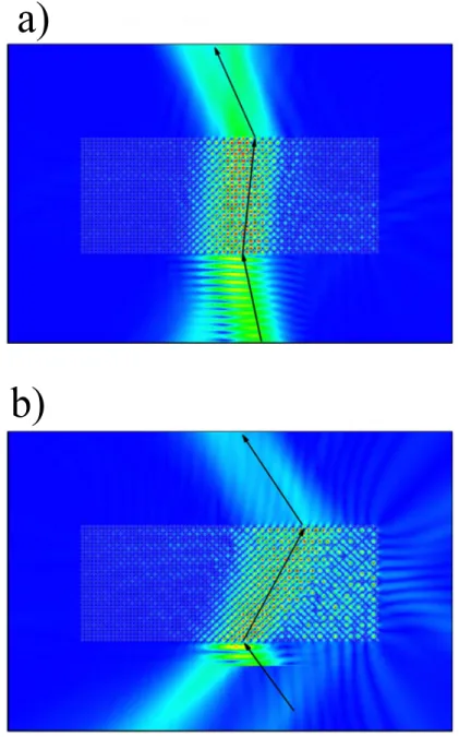
Figure 3. Calculated electric field intensity distributions for incidence angles of 15 degrees and
45 degrees.
demonstrate the negative refraction of electromagnetic waves by the metallodielectric photonic crystal, we calculated the electric field intensities for electromagnetic waves of different incident angles. Figures 3 (a) and (b) shows our results at 9.7 GHz for incidence angles of 15 degrees and 45 degrees, respectively. Even at 45 degrees incidence angle, the electromagnetic waves are negatively refracted.
positive side monopole receiver
horn antenna
negative side
Figure 4. Experimental setup for negative refraction measurement. Electric field intensities are
measured along the surface of the photonic crystal (shown by the dashed line) by a monopole receiver. Origin of the coordinate system is the middle of the surface. Source is a horn antenna. Incidence direction is represented by the arrow.
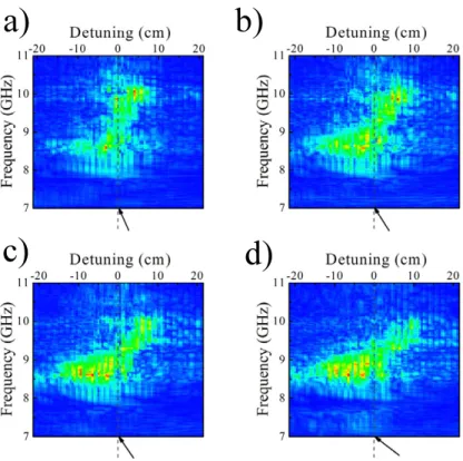
In order to demonstrate the negative refraction effect experimentally, we measured the electric field intensity along the surface of the photonic crystal at the output interface for various incidence angles. The experimental setup consists of transmitting horn antenna and receiving monopole antenna. The schematics of the experimental setup are shown in Fig. 4. When the electromagnetic waves are negatively refracted one expects to observe higher intensities in the negative side of the crystal. Wherever, for positive refraction one expects to observe higher intensities on the positive side of the metallodielectric photonic crystal. Measurement results for incidence angles of 15 degrees, 25 degrees, 35 degrees, and 45 degrees are shown in Fig. 5. Figure 5 shows that between 9.25 and 10.3 GHz waves emerge from the negative side of the PC for all incidence angles. Hence, between 9.25 and 10.3 GHz electromagnetic waves are negatively refracted by the PC.
We further explored the negative refraction effect by measuring the electric field intensities on the output side of the photonic crystal over an area of 40x15 cm2 area. The measurements were carried out by using a precision X-Y stage with steps of 2.5 mm. The measurement results for an incidence angle of 25◦ are shown in Figs. 6 (a) and (b). Figure 6 (a) shows the electric field intensity for 9 GHz. Note that at 9 GHz the incident electromagnetic waves are positively refracted by the metallodielectric photonic crystal. On the other hand, Fig. 6 (b) shows the electric field intensities for 9.7 GHz. Figure 6 (b) clearly demonstrates that the electromagnetic waves are negatively refracted at 9.7 GHz when they are incident by 25◦ on the metallodielectric photonic crystal.
3. Flat lens
Negative refraction effect may be utilized in certain applications. One such application is the focusing of electromagnetic waves. In order to demonstrate the focusing effect, we placed a monopole source is placed in front of the metallodielectric PC. The monopole source was 11 cm away from the surface of the PC. The electric field amplitude distribution on the output side of the metallodielectric photonic crystal was measured by the receiving monopole antenna. The measurements were performed over an area of 40x15 cm2 with steps of 1 mm. Note that in the previous section it was that EM waves with a frequency of 9.7 GHz are negatively refracted by the metallodielectric PC. Since at this frequency EM waves are negatively refracted, one expects to observe the focusing of EM waves emitted from a source at 9.7 GHz. The measured field intensities for 9.7 GHz are shown in Fig. 7. First of all, Fig. 7 shows that the
Figure 5. Measured electric field intensities along the surface of the photonic crystal are shown
for incidence angles of (a) 15◦(b) 25◦ (c) 35◦ (d) 45◦. Incidence direction is shown by the arrow. Black represents the maximum field intensity, whereas white color represents the minimum field intensity.
electromagnetic fields emitted in all directions by the source monopole antenna are focused by the metallodielectric photonic crystal. Moreover, the image formed by the focusing effect is quite sharp. To be explicit, the measured half-width of the intensity profile (along the y-axis) at this frequency is 2.78 cm, which can be compared to the wavelength λ = 3.09 cm at this frequency. Also, note that, the image is elongated along x-axis.
4. Conclusion
In summary, we investigated the negative refraction and focusing effects in metallodielectric photonic crystals. We showed that by adding a dielectric perturbation to the metallic photonic crystal one can increase the range of incidence angles that are negatively refracted. Furthermore, we demonstrated focusing of electromagnetic waves as an application of the negative refraction effect. Intensity profiles at selected frequencies showed that the extent of focusing is at the order of one wavelength. The perturbation scheme we proposed can be utilized to cause the negative refraction effect for use in applications and it provides a method to obtain all-angle negative refraction.
Acknowledgements
This work was supported by EU-DALHM, EU NOE-METAMORPHOSE, EU-NOE-PHOREMOST, TUBITAK, and MSB-KOBRA-002. One of the authors (Ekmel Ozbay) acknowledges partial support from Turkish Academy of Sciences.
Figure 6. a) Electric field intensity for 9 GHz. b) Electric field intensity for 9.7 GHz. Incidence
angle is 25◦.
Figure 7. Measured electric field intensity at the output side of the metallodielectric photonic
crystal. The source monopole was placed on the other side of the photonic crystal. The distance of the source monopole antenna to the input surface of the metallodielectric photonic crystal was 11 cm.
References
[1] E. Yablonovitch, Phys. Rev. Lett.58, 2059 (1987). [2] S. John, Phys. Rev. Lett.58, 2486 (1987).
[3] M. Bayindir, B. Temelkuran, and E. Ozbay, Phys. Rev. B61, R11855-R11858 (2000).
[4] A. Chutinan and S. Noda, Phys. Rev. B62, 4488-4492 (2000).
[5] S. G. Johnson, P. R. Villeneuve, S. Fan, and J. D. Joannopoulos, Phys. Rev. B62, 8212-8222 (2000).
[6] Mehmet Bayindir and E. Ozbay, Appl. Phys. Lett.81, 4514 (2002).
[7] S. Fan, P. R. Villeneuve, J. D. Joannopoulos, and H. A. Haus, Phys. Rev. Lett.80, 960 (1998).
[8] H. Kosaka, T. Kawashima, A. Tomita, M. Notomi, T. Tamamura, T. Sato, and S. Kawakami, Appl. Phys. Lett.74, 1370 (1999).
[9] S. Noda, A. Chutinan, and M. Imada, Nature (London)407, 608 (2000).
[10] Irfan Bulu, Humeyra Caglayan, and Ekmel Ozbay, Appl. Phys. Lett.83, 3263 (2003).
[11] Stefan Enoch, Boris Gralak, and Grard Tayeb, Appl. Phys. Lett.81, 1588 (2002).
[12] M. Notomi, Phys. Rev. B62, 10696 (2000).
[13] S. Foteinopoulou and C. M. Soukoulis, Phys. Rev. B67, 235107 (2003).
[14] Ertugrul Cubukcu, Koray Aydin, Ekmel Ozbay, Stavroula Foteinopoulou, and Costas M. Soukoulis , Nature
423, 604 (2003).
[15] Chiyan Luo, Steven G. Johnson, J. D. Joannopoulos, and J. B. Pendry, Opt. Express11, 746 (2003).
[16] Chiyan Luo, Steven G. Johnson, J. D. Joannopoulos, and J. B. Pendry, Phys. Rev. B65, 201104 (2002).
[17] Boris Gralak, Stefan Enoch, and Grard Tayeb, J. Opt. Soc. Am. A17, 1012 (2000).
[18] Hiroyuki Takeda and Katsumi Yoshino, Jpn. J. Appl. Phys., Part 241, L773 (2002).
[19] Chongjun Jin, Bingying Cheng, Baoyuan Man, Daozhong Zhang, Shouzheng Ban, Bo Sun, Lieming Li, Xiangdong Zhang, and Zhaoqing Zhang, Appl. Phys. Lett. 75, 1201 (1999).
[20] K. Sakoda,Optical Properties of Photonic Crystals, Springer, Germany, (2001). 40