we demonstrated the focusing of electromagnetic waves by the use of a metallodielectric photonic crystal. We obtained focusing of electromagnetic waves away from the surface of the photonic crystal. The observed focusing points are found to be larger than one wavelength away from the photonic crystal interface.
DOI:10.1103/PhysRevB.72.045124 PACS number共s兲: 42.70.Qs
Since the pioneering work of Yablonovitch1 and John2 photonic crystals have attracted a great deal of interest. One of the major reasons for this interest is the rich dispersion relations of the photonic crystals. Dispersion properties of photonic crystals provide various means to control the propa-gation of electromagnetic 共EM兲 waves. In this sense many applications such as waveguides,3–5 wavelength division multiplexing共WDM兲,6–9and highly directional antennas10,11 have been proposed and demonstrated.
An interesting phenomenon arising from the dispersion relation of photonic crystals is the so-called negative refrac-tion effect.12–17This effect is observed for frequency ranges at which the wave vector of the incident waves and the group velocity of the transmitted waves fell into the opposite sides of the interface normal.12 As a result, for such frequency ranges the photonic crystal behaves as if the index of refrac-tion is negative.
In order to make use of the negative refraction effect in certain applications such as focusing of electromagnetic waves, one usually requires negative indices of refraction over a wide range of angles. To obtain negative indices of refraction over a wide range of angles is still a major chal-lenge for photonic-crystal-based structures.14–16In this paper we address this issue by using a metallodielectric photonic crystal. We show that by adding a periodic dielectric pertur-bation to the metallic photonic crystal共PC兲, one can increase the range of angles at which negative indices of refraction prevail. Furthermore, as an application of the negative refrac-tion effect we demonstrat the focusing effect.
Previously, Luo et al.15 used a similar approach to shift the equal-frequency-surface共EFS兲 contours in the frequency axes, and theoretically demonstrated all-angle negative re-fraction by embedding metallic rods arranged in a square lattice into a high-dielectric-constant medium for TM-polarized 共electric field parallel to the axis of rods兲 EM waves. The effect of using a high-dielectric-constant host medium for metallic rods is to increase the effective index of the medium. This results in lowering the EFS contours in frequency, while keeping the area occupied by the EFS con-tours in the k space unchanged. Apart from manufacturing difficulties, this approach has some disadvantages. One of these disadvantages is that one has to carefully terminate the
surface of the PC. Without a proper termination, the corru-gation on the surface of the PC may lead to surface modes.18–20In addition, EM waves incident on the surface of the PC structure will be first refracted by the high-dielectric-constant host medium. Because of the high index of the host medium, EM waves will be refracted toward the surface nor-mal vector共⌫-M direction for a square lattice tilted by 45°兲. This refracted beam will be further refracted by the PC struc-ture. EM waves with wave vector directed along the ⌫-M direction will be refracted along the surface normal vector by the PC structure. As a result the output beam will be directed along the surface normal vector. In our approach, we use a periodic dielectric constant perturbation instead of a high-dielectric-constant host medium. Periodic dielectric constant perturbation is achieved by adding a dielectric rod to each unit cell of the metallic PC. Our approach has two major advantages. First of all there is no ambiguity on how to ter-minate the surface and manufacturing is relatively easy. Sec-ond, the problem that we discussed due to the refraction by the high-dielectric-constant host medium is not present in our structure.
The metallodielectric photonic crystal that we used in our experiments and calculations is a square lattice of metallic and dielectric rods. The basis of the crystal consists of a metallic and a dielectric rod placed along the diagonal of the square unit cell关inset of Fig. 1共b兲兴. Cylindrical alumina rods with a radius of 1.55 mm are used for the dielectric rods and in the frequency range of interest the dielectric constant of alumina is 9.61. The metallic共aluminum兲 rods have a radius of 1.5 mm. Both the metallic and dielectric rods have a height of 15 cm.
One way to view the metallodielectric photonic crystal, especially in the microwave region, is to consider it as a metallic photonic crystal with a periodic dielectric perturba-tion. It is expected that an attractive perturbation, which cor-responds to a positive dielectric constant, will result in low-ering of bands.21,22The computed band structures 共for TM polarization: electric field is parallel to the axis of rods兲 for a metallic photonic crystal and a metallodielectric photonic crystal with the same lattice parameters are shown in Figs. 1共a兲, 1共b兲, and 1共c兲 and 5共d兲, respectively. We considered TM-polarized EM waves in our calculations and
experi-ments. The dielectric rod used in the calculations is alumina and has a dielectric constant of 9.61. The radius of the di-electric rod is 0.136a, where a is the lattice constant. The metallic rod is aluminum and has a radius of 0.14a. Figure 1共b兲 shows that the bands of the metallodielectric photonic crystal are lowered compared to the bands of the metallic photonic crystal关Fig. 1共a兲兴. For comparison we have calcu-lated the first three bands of a photonic crystal composed of dielectric rods in a square array关Fig. 1共c兲兴 and a perturbed dielectric crystal with two dielectric rods with different di-electric constants关Fig. 1共d兲兴. The unperturbed dielectric PC is composed of alumina rods in a square lattice. The per-turbed dielectric PC is obtained by adding a dielectric rod, whose dielectric constant is three times smaller than that of alumina, to the unit cell of the unperturbed dielectric PC. The second and third bands of the perturbed dielectric crystal are appreciably lowered compared to the unperturbed dielectric photonic crystal. However, the first band is only slightly low-ered. This can be explained by the fact that the first band is a dielectric band. Since the electric field intensities of these modes have appreciable values only inside the dielectric ma-terial, these modes are slightly affected by the perturbation.
Conservation of the surface parallel component of the wave vector suggests that one way to increase the range of negatively refracted incidence angles is to reduce the radius of free-space equal-frequency contour. This can be achieved by choosing a lower frequency range at which one expects negative refraction. In addition, the shape and the size of the equal-frequency contours for the photonic crystal must be kept unchanged. Hence, lowering the bands without modify-ing the lattice parameters such as reducmodify-ing the lattice con-stant increases the range of incidence angles that are nega-tively refracted.
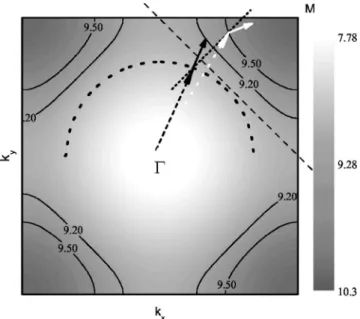
The computed band structure of the metallodielectric pho-tonic crystal for TM polarization over the first Brillouin zone is plotted in Fig. 2. The free-space equal-frequency contour 共dotted circle in Fig. 2兲 and equal-frequency contours
corre-sponding to negative refraction are also plotted. The surface of the photonic crystal is aligned such that the normal vector to the air–photonic crystal interface is along the⌫-M direc-tion. The wave vectors of the transmitted waves are found from the conservation of the surface-parallel component of the wave vector. Figure 2 shows that for the plotted equal-frequency contours, the group velocity of the incident waves and the group velocity of the transmitted waves fall on op-posite sides of the surface normal. Correspondingly, these waves are negatively refracted. For the plotted equal-frequency contours, the magnitude of the largest surface-parallel wave vector component in free space is smaller than the largest surface-parallel wave vector component in the photonic crystal. In addition, the group velocities in free space and the group velocities in the photonic crystal fall on different sides of the surface normal. As a result, for the plotted equal-frequency contours EM waves are negatively refracted for all incidence angles.
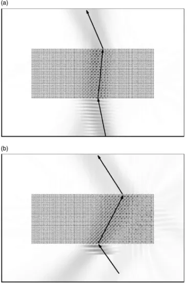
We calculated the electric field amplitude distributions for TM polarized waves incident on the metallodielectric PC for various incidence angles. Figure 3 shows the steady-state electric field amplitudes at 9.7 GHz for incidence angles of 15° and 45°. The incident wave is a Gaussian beam and has a width of three wavelengths. The equal-frequency contour shown in Fig. 2 indicates that at this frequency the metall-odielectric photonic crystal may exhibit negative refraction, i.e., incident and transmitted electromagnetic waves fall on the same side of the surface normal. The negative refraction effect is clearly observed in Fig. 3.
FIG. 1. The first three TM-polarized bands for共a兲 the metallic photonic crystal,共b兲 the metallodielectric photonic crystal, 共c兲 the unperturbed dielectric photonic crystal, and 共d兲 the perturbed di-electric photonic crystal.
FIG. 2. Equal-frequency contours共solid curves兲 are shown for the metallodielectric photonic crystal. Crystal orientation is shown by the dashed line. Dotted circle represents the free-space equal-frequency contour at 9.5 GHz. Frequencies are shown in gigahertz. Long dashed arrow with black color represents the free-space wave vector whereas the short black arrow represents the free-space group velocity. Long dashed arrow with white color represents the wave vector of the refracted waves in the photonic crystal. Small white colored arrow indicates the direction of the group velocity inside photonic crystal.
To demonstrate the negative refraction effect experimen-tally, one can measure the electric field intensity along the surface of the photonic crystal at the output interface for various incidence angles. A sample measurement setup is shown in Fig. 4. In this configuration, the transmitting horn antenna is tilted such that EM waves are incident on the
louin zone. As a result兩kfree兩 is smaller than any reciprocal lattice vector兩Gn兩. Hence, the condition of a single refracted beam is satisfied for the considered frequency range. The other criterion to be met is that there must not be surface propagating waves in the frequency range of interest. The surface propagating waves may be due to surface corrugation18,19 or surface plasmon modes of the metallic rods.24 There are no corrugations at the surface of the met-allodielectric PC that we have used. In addition, surface plas-mon modes of the metallic rods occur for the TE-polarized 共electric field perpendicular to the axes of the rods兲 waves.23 As a result there are no surface propagating waves for the structure that we used in this study. Also, our FDTD calcu-lations shown in Fig. 3 clearly show that a single refracted beam propagates inside the photonic crystal and there are no distinguishable surface propagating waves. In conclusion, the experimental scheme depicted in Fig. 4 can be used to demonstrate negative refraction for this structure.
We measured the electric field intensities along the sur-face of the photonic crystal for various incidence angles to demonstrate the negative refraction experimentally. We used a HP-8510 C vector network analyzer in our measurements. Electromagnetic waves are transmitted by a standard gain horn antenna and measured by a monopole antenna. The in-cidence direction is indicated by a long arrow and the surface normal is indicated by the dashed line. Waves that are posi-tively refracted are expected to emerge from the positive side of the surface, whereas negatively refracted waves are to emerge from the negative side. Measurement results for in-cidence angles of 15°, 25°, 35°, and 45° are shown in Figs. 5共a兲, 5共b兲, 5共c兲, and 5共d兲, respectively. Figure 5 shows that between 9.25 and 10.3 GHz waves emerge from the negative side of the PC. Hence, between 9.25 and 10.3 GHz EM waves are negatively refracted by the PC. By using the shift with respect to the center of the PC surface one can calculate the indices of refraction. The sign of the index of refraction is decided by whether the shift is to the positive side or to the negative side. Experimental and theoretical results for the indices of refraction at 25° incidence angle are shown in Fig. 6. The indices of refraction are positive between 9 and 9.19 GHz. Around 9.2 GHz there is an abrupt change: just below 9.2 GHz the indices of refraction are positive and just above 9.2 GHz the indices of refraction are negative. Moreover, in the close vicinity of 9.2 GHz the indices of refraction are very high, +18 and −12. This is due to the flatness of EFS contours around 9.2 GHz共Fig. 2兲. Between 9.25 and 10 GHz indices of refraction are negative. Figure 6 shows that the indices of refraction are strongly dependent on frequency at
FIG. 3. Electric field distribution for incidence angle共a兲 15° and 共b兲 45°. Black represents the maximum field amplitude, whereas white color represents the minimum field amplitude.
FIG. 4. Experimental setup for negative refraction measurement. Electric field intensities are measured along the surface of the pho-tonic crystal共shown by the dashed line兲 by a monopole receiver. Origin of the coordinate system is the middle of the surface. Source is a horn antenna. Incidence direction is represented by the arrow.
fixed incidence angle. In addition, due to the anisotropic EFS contours shown in Fig. 2 one expects indices of refraction to be dependent on the incidence angle. Measured indices of refraction at fixed frequency, 9.7 GHz, for incidence angles of 15°, 25°, 35°, and 45° are −0.65, −0.85, −0.88, and −0.96, respectively. These results clearly show that incidence-angle-independent indices of refraction cannot be defined for the metallodielectric photonic crystal used in this study. This is due to the shape of the EFS contours near the frequencies where one observes negative refraction 共Fig. 2兲. To obtain uniform angle-independent negative indices of refraction two
conditions must be satisfied. First, a circular EFS centered at the origin of the Brillouin zone is required. Second, the ra-dius of circular EFS must be decreasing with increasing fre-quency.
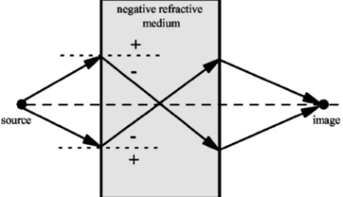
Negative refraction effect may be utilized in certain ap-plications. One such application is the focusing of electro-magnetic waves.14,25–27An illustration of this effect by using simple ray optics arguments is given in Fig. 7. Two rays emerging from a point source will be refracted to the nega-tive side of the surface normal as they impinge on the pho-tonic crystal. On the other side of the phopho-tonic crystal–air interface, EM waves will be once more refracted toward the negative side of the surface normal. As a result two rays will intersect at a point. At the intersection point an image of the source will be formed. We will call this point the image point or focus point throughout the rest of the paper.
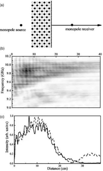
Focusing of EM waves emitted from a monopole source is theoretically demonstrated in Fig. 8. A monopole source is placed in front of the metallodielectric PC. The monopole source is 11 cm away from the surface of the PC. The elec-tric field amplitude distribution is calculated by using the FDTD method at 9.7 GHz. It was shown in Fig. 5 that EM waves with a frequency of 9.7 GHz are negatively refracted by the metallodielectric PC. Since at this frequency EM waves are negatively refracted, one expects to observe the focusing of EM waves emitted from a source at 9.7 GHz. Figure 8 shows that EM waves emitted from the monopole source are focused both inside the PC and outside the PC. This is consistent with the simple ray optics scheme shown in Fig. 7. The electric field intensity along the dashed line 关Fig. 8共a兲兴 is shown in Fig. 8共b兲. Figure 8共b兲 indicates that the image formed outside the PC is located at a distance 13 cm away from the metallodielectric PC. The electric field intensity along the dotted line 关Fig. 8共a兲兴 is shown in Fig. 8共c兲. Figures 8共b兲 and 8共c兲 show that an image of the mono-pole source is formed at a distance of 13 cm away from the surface of the PC. The half-power beam width is 2.6 cm. This may be compared to the wavelength at 9.7 GHz, 3.09 cm.
We measured the electric field intensity along the normal vector of the surface to demonstrate the focusing effect ex-perimentally. The experimental setup is shown in Fig. 9共a兲. A monopole source is placed in front of the photonic crystal and the electric field intensity is measured on the other side of the photonic crystal along the direction indicated by the
FIG. 5. Measured electric field intensities along the surface of the photonic crystal are shown for incidence angles of共a兲 15°, 共b兲 25°,共c兲 35°, and 共d兲 45°. Incidence direction is shown by the arrow. Black represents the maximum field intensity, whereas white color represents the minimum field intensity.
FIG. 6. Measured and calculated indices of refraction between 9 and 10 GHz at 15° incidence angle. Solid curve represents the ex-perimental data and the dashed curve represents the theoretical in-dices of refraction obtained from finite-difference time-domain 共FDTD兲 simulations.
arrow. Measurement results for a source distance 11 cm away from the surface of the photonic crystal are shown in Fig. 9共b兲. Figure 9共c兲 shows the calculated and measured intensity profiles at 9.7 GHz. Note that the measurement and simulation results are in quite good agreement. Figure 9共c兲 shows that although an image of the source is formed on the other side of the PC, the extent of the image is not sharp along the direction of the surface normal when compared to the wavelength. This is mainly due to two reasons. First, the index of refraction is an anisotropic function of incidence angle. Second, the index of refraction is different from −1. To observe a correct image of the source an index of refrac-tion equal to −1 at all incidence angles is required.28 To further investigate the focusing effect we also measured
elec-FIG. 8. 共a兲 Electric field distribution from a monopole source placed in front of the metallodielectric PC. Black represents the maximum field amplitude, whereas white color represents the mini-mum field amplitude.共b兲 Electric field intensity along the dashed line in共a兲. 共c兲 Electric field intensity along the dotted line in 共a兲.
FIG. 9. 共a兲 Experimental setup for focusing measurement. Both the receiver and the source are monopole antennas. Electric field intensities are measured along the direction shown by the arrow.共b兲 Electric field intensities for when the source is placed 11 cm away from the photonic crystal. Black represents the maximum field in-tensity, whereas white color represents the minimum field intensity. 共c兲 Measured and calculated electric field intensities at 9.7 GHz.
FIG. 10. 共a兲 Electric field intensities measured at a distance of 13 cm away from the surface of the photonic crystal. Measurement direction is along the surface of the photonic crystal. Measurement is performed at 9.7 GHz.
tric field intensities parallel to the surface of the photonic crystal around the image point. The experimental setup is similar to that of Fig. 9共a兲, except that the intensities are measured parallel to the surface of the PC near the image point. Such a measurement provides information about the extent of the focusing. Measurement and calculation results at 9.7 GHz when the source is placed 11 cm away from the PC surface are shown in Fig. 10. For this case the image point is at 13 cm away from the surface of the photonic crystal. Figure 10 shows that the electric field intensities are confined to a narrow region at 9.7 GHz. To be explicit, the measured half-width of the intensity profile at this frequency is 2.78 cm, which can be compared to the wavelength = 3.09 cm at this frequency. Note that the image formed is not a “stigmatic image” or “sharp image” as defined in optics.29 The image of the point source is deformed due to the anisotropic negative indices of refraction. The deforma-tion is also due to the indices of refracdeforma-tion being different from −1. As a result, the metallodielectric PC introduces spa-tial aberration to the image. This effect can be compared to
the caustic effects.30,31 Our results clearly shows that one requires isotropic n = −1 indices of refraction for better im-aging.
In summary, we investigated the negative refraction and focusing effects in metallodielectric photonic crystals. We showed that by adding a dielectric perturbation to the metal-lic photonic crystal one can increase the range of incidence angles that are negatively refracted. Furthermore, we demon-strated focusing of electromagnetic waves as an application of the negative refraction effect. Intensity profiles at selected frequencies showed that the extent of focusing is at the order of one wavelength. The perturbation scheme we proposed can be utilized to cause the negative refraction effect for use in applications and it provides a method to obtain all-angle negative refraction.
This work was supported by EU-DALHM, EU NOE-METAMORPHOSE, EU-NOE-PHOREMOST, TUBITAK, and MSB-KOBRA-002. One of the authors共E.O.兲 acknowl-edges partial support from Turkish Academy of Sciences.
*Electronic address: [email protected]
1E. Yablonovitch, Phys. Rev. Lett. 58, 2059共1987兲. 2S. John, Phys. Rev. Lett. 58, 2486共1987兲.
3M. Bayindir, B. Temelkuran, and E. Ozbay, Phys. Rev. B 61,
R11855共2000兲.
4A. Chutinan and S. Noda, Phys. Rev. B 62, 4488共2000兲. 5S. G. Johnson, P. R. Villeneuve, S. Fan, and J. D. Joannopoulos,
Phys. Rev. B 62, 8212共2000兲.
6M. Bayindir and E. Ozbay, Appl. Phys. Lett. 81, 4514共2002兲. 7S. Fan, P. R. Villeneuve, J. D. Joannopoulos, and H. A. Haus,
Phys. Rev. Lett. 80, 960共1998兲.
8H. Kosaka, T. Kawashima, A. Tomita, M. Notomi, T. Tamamura,
T. Sato, and S. Kawakami, Appl. Phys. Lett. 74, 1370共1999兲.
9S. Noda, A. Chutinan, and M. Imada, Nature共London兲 407, 608
共2000兲.
10I. Bulu, H. Caglayan, and E. Ozbay, Appl. Phys. Lett. 83, 3263
共2003兲.
11S. Enoch, B. Gralak, and G. Tayeb, Appl. Phys. Lett. 81, 1588
共2002兲.
12M. Notomi, Phys. Rev. B 62, 10696共2000兲.
13S. Foteinopoulou and C. M. Soukoulis, Phys. Rev. B 67, 235107
共2003兲.
14E. Cubukcu, K. Aydin, E. Ozbay, S. Foteinopoulou, and C. M.
Soukoulis, Nature共London兲 423, 604 共2003兲.
15C. Luo, S. G. Johnson, J. D. Joannopoulos, and J. B. Pendry, Opt.
Express 11, 746共2003兲.
16C. Luo, S. G. Johnson, J. D. Joannopoulos, and J. B. Pendry,
Phys. Rev. B 65, 201104共R兲 共2002兲.
17B. Gralak, S. Enoch, and G. Tayeb, J. Opt. Soc. Am. A 17, 1012
共2000兲.
18R. D. Meade, K. D. Brommer, A. M. Rappe, and J. D.
Joannopo-ulos, Phys. Rev. B 44, 10961共1991兲.
19F. Ramos-Mendieta and P. Halevi, Phys. Rev. B 59, 15112
共1999兲.
20S. Xiao, M. Qiu, Z. Ruan, and S. He, Appl. Phys. Lett. 85, 4269
共2004兲.
21H. Takeda and K. Yoshino, Jpn. J. Appl. Phys., Part 2 41, L773
共2002兲.
22C. Jin, B. Cheng, B. Man, D. Zhang, S. Ban, B. Sun, L. Li, X.
Zhang, and Z. Zhang, Appl. Phys. Lett. 75, 1201共1999兲.
23K. Sakoda, Optical Properties of Photonic Crystals 共Springer,
Germany, 2001兲.
24T. Ito and K. Sakoda, Phys. Rev. B 64, 045117共2001兲. 25P. V. Parimi, W. T. Lu, P. Vodo, and S. Sridhar, Nature共London兲
426, 404共2003兲.
26I. V. Shadrivov, A. A. Sukhorukov, and Y. S. Kivshar, Appl.
Phys. Lett. 82, 3820共2003兲.
27Z.-Y. Li and L.-L. Lin, Phys. Rev. B 68, 245110共2003兲. 28A. Martinez, H. Miguez, A. Griol, and J. Marti, Phys. Rev. B 69,
165119共2004兲.
29M. Born and E. Wolf, Principles of Optics: Electromagnetic
Theory of Propagation, Interference and Diffraction of Light,
7th ed.共Cambridge University Press, Cambridge, U.K., 1999兲.
30J. A. Lock and J. R. Woodruff, Am. J. Phys. 57, 260共1989兲. 31J. A. Lock and J. H. Andrews, Am. J. Phys. 60, 397共1992兲.