First-principles study of defects and adatoms in silicon carbide honeycomb structures
E. Bekaroglu,1M. Topsakal,1S. Cahangirov,1and S. Ciraci1,2,*
1UNAM–Institute of Materials Science and Nanotechnology, Bilkent University, Ankara 06800, Turkey 2Department of Physics, Bilkent University, Ankara 06800, Turkey
共Received 3 December 2009; revised manuscript received 1 February 2010; published 24 February 2010兲 We present a study of mechanical, electronic and magnetic properties of two-dimensional共2D兲, monolayer of silicon carbide共SiC兲 in honeycomb structure and its quasi-one-dimensional 共quasi-1D兲 armchair nanorib-bons using first-principles plane-wave method. In order to reveal dimensionality effects, a brief study of three-dimensional共3D兲 bulk and 1D atomic chain of SiC are also included. Calculated bond-lengths, cohesive energies, charge transfers and band gaps display a clear dimensionality effect. The stability analysis based on the calculation of phonon frequencies indicates that 2D SiC monolayer is stable in planar geometry. We found that 2D SiC monolayer in honeycomb structure and its bare and hydrogen passivated nanoribbons are ionic, nonmagnetic, wide band gap semiconductors. The band gap is further increased upon self-energy corrections. The mechanical properties are investigated using the strain energy calculations. The effect of various vacancy defects, adatoms, and substitutional impurities on electronic and magnetic properties in 2D SiC monolayer and in its armchair nanoribbons is also investigated. Some of these vacancy defects and impurities, which are found to influence physical properties and attain magnetic moments, can be used to functionalize SiC honeycomb structures.
DOI:10.1103/PhysRevB.81.075433 PACS number共s兲: 73.22.⫺f, 75.75.⫺c, 63.22.⫺m
I. INTRODUCTION
Owing to its exceptional thermal and physical properties,1
silicon carbide 共SiC兲 is a material, which is convenient for high temperature and high power device applications. Be-cause of its wide band gap, SiC bulk structure has been a subject of active study in optical and optoelectronic research. Unlike the polymorphs of carbon, SiC is a polar material. In spite of the fact that both constituents of SiC are Group IV elements, charge is transferred from Si to C due to higher electronegativity of C relative to Si atom.
Bulk SiC has six commonly used stacking configurations denoted as 3C共zincblende兲, 2H 共wurtzite兲, 4H, 6H, 15R, and 21R. Lubinsky et al.2reported optical data related with indi-rect transitions, dielectric function and reflectivity of 3C SiC using first-principles Hartree-Fock-Slater method. A more comprehensive study3using orthogonalized linear
combina-tion of atomic orbitals共OLCAOs兲 method comprises the cal-culations of lattice constants, electronic band structure and optical properties of all six stacking configuration of SiC.
As for SiC in lower dimensionality, SiO2 coated SiC nanowires4 were synthesized and showed favorable
photo-catalytic behavior. A theoretical work on hydrogen passi-vated SiC nanowires5provided the energy bands both using
local density approximation within density functional theory 共DFT兲 and sp3sⴱ LCAO tight binding 共TB兲 methods. SiC-ZnS core-shell structures were also fabricated.6 Zincblende
SiC nanoparticles were synthesized by carbothermal reduc-tion method.7 Band gap of zincblende nanoparticles were
estimated to be around 3 eV from photoluminescence mea-surements. With a similar carbothermal method, microribbons8 with widths in the range of 500 nm– 5 m
and thickness of 50–500 nm were synthesized.
SiC is frequently used as a substrate to grow other materials.9,10 Few layers of graphene was also grown on
SiC.11 SiC clusters共Si
nCn, n = 1 – 10兲 were investigated12
us-ing DFT. With the aim of developus-ing a material for future nanoelectronic applications, binding energy, HOMO-LUMO gap, Mulliken charge, vibrational spectrum and ionization potential of SinCn clusters are revealed.
Earlier, planar honeycomb structure of graphite was ex-foliated and its physical properties were analyzed.13–15While
graphene is a strictly planar crystal, the planar honeycomb structure of Si is unstable, but it is stabilized through puckering.16 Since the honeycomb structure is common to
both C and Si, one expects that stable 2D SiC in honeycomb structure can be synthesized.
In this paper, a comprehensive analysis of the atomic, electronic and magnetic properties of two-dimensional共2D兲 monolayer of SiC honeycomb structure and its bare and hy-drogen passivated armchair nanoribbons共A-SiCNR兲 are car-ried out using first-principles calculations. In spite of the fact that 2D SiC monolayer is not synthesized yet, this study demonstrates its stability based on reliable theoretical meth-ods. Furthermore, various mechanical, electronic, and mag-netic properties are revealed. We started with the discussion of three-dimensional 共3D兲 zincblende and wurtzite crystals, as well as SiC atomic chain as an ultimate one-dimensional 共1D兲 system; we presented an analysis of optimized atomic structures with corresponding phonon dispersion curves and electronic energy band structures and effective charges. Then we provided an extensive analysis of 2D and quasi-1D 共na-noribbon兲 SiC in terms of the optimized atomic structures and their stability, electronic, and magnetic structures. We revealed elastic constants, such as in-plane stiffness and Poisson’s ratio. Having obtained the results for 1D, 2D, and 3D structures, we presented a comprehensive discussion of dimensionality effects. Then we investigated the effect of vacancy defects 共such as Si and C vacancy, Si+C vacancy and C-Si antisite defect兲 on the electronic and magnetic properties of single layer SiC and its armchair nanoribbons. Furthermore, we showed that SiC can be functionalized through adsorption of a foreign atom to the surface of 2D
SiC or through substitution of either C or Si with a foreign atom. It is revealed that 2D SiC and its ribbons provide un-usual physical properties, which are absent in 3D SiC crys-tals. For example, while various allotropic forms of SiC in-cluding its honeycomb structures are normally nonmagnetic semiconductors, a Si vacancy gives rise to spin polarization. Significant variation in the band gap of narrow A-SiCNR’s with their widths may be crucial in designing optoelectronic nanodevices.
II. MODEL AND METHODOLOGY
We have performed first-principles plane-wave calcula-tions within DFT using PAW potentials.17 The
exchange-correlation potential has been approximated by generalized gradient approximation共GGA兲 using PW91 共Ref. 18兲 func-tional both for spin-polarized and spin-unpolarized cases. For the sake of comparison, the calculations are also carried out using different potentials and exchange-correlation ap-proximations. All structures have been treated within the su-percell geometry using the periodic boundary conditions. A plane-wave basis set with kinetic energy cutoff of 500 eV has been used. A vacuum spacing of 12 Å hinders the inter-actions between SiC monolayers in adjacent supercells. In the self-consistent structure optimizations, the Brillouin zone 共BZ兲 is sampled by, respectively, 共5⫻5⫻5兲, 共11⫻11⫻1兲, and 共11⫻1⫻1兲 special k points for 3D bulk, 2D honey-comb, and 1D nanoribbons of SiC. Further relaxation is made with 共11⫻11⫻11兲, 共31⫻31⫻1兲, and 共25⫻1⫻1兲 special k points in order to find the final structure. All atomic positions and lattice constants are optimized by using the conjugate gradient method, where the total energy and atomic forces are minimized. The convergence for energy is chosen as 10−5 eV between two steps and the maximum Hellmann-Feynman forces acting on each atom is less than 0.04 eV/Å upon ionic relaxation. The pseudopotentials cor-responding to four valence electrons of Si共Si:3s23p2兲 and C 共C:2s22p2兲 are used. Numerical plane-wave calculations are performed by using VASP.19,20 Part of the calculations have also been repeated by using SIESTA共Ref. 21兲 software. The cohesive energy of any SiC structure is found as EC = ET关SiC兴−ET关Si兴−ET关C兴 in terms of the optimized total en-ergy of any SiC structure, and the spin-polarized total ener-gies of free Si and C atoms, all calculated in the same super-cell using the same parameters. Phonon calculations were carried out using PHONprogram22 implementing force
con-stant method. GW0calculations23are again handled byVASP.
III. 1D ATOMIC CHAIN AND 3D BULK CRYSTAL OF SIC
In this section, we present a brief discussion of 1D SiC atomic chain and 3D bulk crystal based on our structure
op-timized total energy and phonon spectrum calculations. Stud-ies on SiC bulk lattice and atomic chains already exist in the literature.2,3,24However, our purpose is to carry out
calcula-tions with same parameters as used in 2D monolayer SiC honeycomb structure and provide a consistent comparison of dimensionality effects.
A. 1D SiC Chains
Earlier, the first theoretical study of atomic chains of Groups IV and III-V binary compounds were reported by Senger et al.24 They examined SiC atomic chain as a
func-tion of lattice parameter and found that the wide zigzag atomic chain of SiC with bond angle of⬃147° is energeti-cally more favorable than the linear and narrow angle zigzag chains. Present calculations find that the atomic chains of SiC are nonmagnetic. Calculated structural parameters, cohe-sive energies, band gap, and phonon modes of linear and zigzag atomic chains, which are relevant for the present study are given in Table I. The charge transfer from Si to C is calculated to be ␦q = 2.28 electrons using the Bader analysis.25 Phonon modes calculated with force constant
method have imaginary frequencies. In Fig.1two acoustical and two optical branches of linear SiC chain have imaginary frequencies. Also wide angle zigzag SiC chain has one opti-cal and one acoustiopti-cal branch with imaginary frequencies. These results indicate that free standing SiC chains are not stable. We note that carbon and BN atomic chains are found to be stable and have linear structure.24,26,27 Stability of
lin-ear chain structure is assured bybonding between adjacent atoms.
B. 3D SiC Crystals
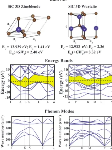
Our work on bulk SiC includes wurtzite 共wz兲 and zincblende 共zb兲 structures. Atoms in wz- and zb-SiC are fourfold coordinated through tetrahedrally directed sp3 orbit-als. Calculated structural parameters, cohesive energies, en-ergy band structures and phonon modes are given in Fig.2. Zincblende SiC structure in Td symmetry has cubic lattice constants, a1= a2= a3= 3.096 Å. Si-C bond distance d is 1.896 Å. Each Si共C兲 is connected to its four nearest neigh-bor C 共Si兲; four Si-C bonds are equal. Charge transfer from Si to C is␦q = 2.59 electrons calculated via Bader analysis.25
While the GGA band gap is 1.41 eV, it increases to 2.40 eV after GW0corrections. As for wz-SiC crystal, the hexagonal lattice constants of the optimized structure in equilibrium are
a1= a2= 3.091 Å, c/a=1.642. The small deviation of c/a from the ideal value of 1.633 imposes a slight anisotropy on the lengths of tetrahedrally directed Si-C bonds. While the length of three short bonds is 1.893 Å, the fourth bond is TABLE I. Si-C bond length d, lattice constant a, bond angle␣, charge transfer from Si to C␦q, band gap
EG, and cohesive energy ECvalues for two different types of SiC chains.
Type d 共Å兲 a 共Å兲 共deg.兲␣ ␦ q 共e兲 EG 共eV兲 EC 共eV兲 Linear 1.649 3.298 180 2.28 2.00 8.962 Wide zigzag 1.673 3.268 155.2 2.15 1.18 8.968
slightly longer and has the length of 1.907 Å. Charge trans-fer from Si to C is␦q = 2.63 electrons. The GGA band gap is
2.36 eV, but it increases to 3.32 eV after GW0correction. The calculated structural parameters and energy band gaps are in reasonable agreement with the earlier calculations and ex-perimental measurements.3,28In particular, the band gap
val-ues of 2.39 and 3.33 eV for zb and wz SiC, respectively are in excellent agreement with the present GW0 corrected val-ues.
The frequencies of phonon modes and their dispersions are calculated for zb and wz crystals by direct共or force con-stant兲 method.22 At long wavelengths near the ⌫ point, the
electric field due to dipoles is critical for phonon modes. This effect lifts the degeneracy between longitudinal and trans-verse optical modes. However the splitting 共known as LO-TO splitting兲 cannot be observed with the direct method used in the present study. Therefore, in Fig.2the highest and second highest optical branches become degenerate at ⌫ point. Present results are in agreement with earlier phonon calculations.29,30
IV. 2D SIC HONEYCOMB STRUCTURE
Two-dimensional monolayer of SiC hexagonal structure of SiC is optimized using periodically repeating supercell having 12 Å spacing between SiC planes. The minimum of total energy occurred when Si and C atoms are placed in the same plane forming a honeycomb structure. The magnitude of the Bravais lattice vectors of the hexagonal lattice is found to be a1= a2= 3.094 Å共see Fig.3兲, and the Si-C bond length to be d = 1.786 Å. The planar structure of 2D SiC is tested by displacing Si and C atoms arbitrarily from their equilib-rium positions by 0.5 Å and then reoptimizing the structure. Upon optimization, the displaced atoms returned to their original positions in the same plane implying the stability of planar structure. Further details on the stability of this struc-ture will be provided with phonon calculations at the end of this section. Two-dimensional monolayer SiC is found to be a semiconductor with a band gap of 2.53 eV within GGA. Furthermore, in Table II, we present lattice constant, bond length, cohesive energy, energy gap values of 2D SiC mono-layer calculated with different potentials. Since DFT usually underestimates the band gap of semiconductors, we also cor-rected the GGA band gap using GW0correction and found it to be 3.90 eV. The charge transfer from Si to C in 2D SiC is calculated to be ␦q = 2.53 electrons. The Si-C bond length FIG. 1. 共Color online兲 Atomic structures, electronic energy
bands, and dispersion of phonon modes of linear and wide angle zigzag SiC atomic chains. EC and EGare cohesive and band gap energies, respectively. Si and C atoms are shown by blue/large and brown/small balls, respectively. Zero of the energy is set to the Fermi energy, EF. SiC 3D Zincblende -15 -10 -5 0 5 10 Energy (eV ) SiC 3D Wurtzite Γ X L K Γ L W A Γ K M L -15 -10 -5 0 5 10 EC= 12.939 eV; EG= 1.41 eV c a1 a2 a1 a2 a3 Γ X Γ L 200 400 0 600 800 Γ K M A Bulk SiC EC= 12.933 eV; EG= 2.36 W ave number (cm -1) W ave number (cm -1) Energy (eV) Energy Bands Phonon Modes EG(+GW0) = 2.40 eV EG(+GW0) = 3.32 eV 200 400 0 600 800 Γ K A
FIG. 2. 共Color online兲 Optimized atomic structure with relevant structural parameters, corresponding energy band structure and fre-quencies of phonon modes of 3D bulk SiC in zincblende and wurtz-ite structures. Zero of energy of the band structure is set at the Fermi level, and band gap is shaded.
and the band gap values in the first row obtained by using GGA+ PAW are in agreement with earlier DFT calculations.31
In addition to structural and electronic properties, we also investigated the mechanical properties of 2D SiC.32–34 One
can specify the mechanical properties of SiC honeycomb sheet in terms of uniaxial strain,⑀=⌬c/c, c being the lattice constant; Poisson’s ratio = −⑀trans/⑀axial and in-plane stiff-ness, C =A1
0共
2E s
⑀2兲. Here A0is the equilibrium area of the
sys-tem and Esis the strain energy calculated by subtracting the total energy of the strained system from the equilibrium total energy. To calculate the elastic constants of monolayer SiC honeycomb structure we switch to rectangular unit cell and consider a large 共8⫻4兲 supercell comprising 32 primitive unit cells. In the harmonic region Es共⑀兲 is first calculated on a 2D grid. The numerical data are then fitted to the expres-sion, Es= A1⑀x
2 + A2⑀y
2
+ A3⑀x⑀y; where⑀xand⑀y are the small strains along x and y directions. In the harmonic region, as a result of the isotropy A1= A2. More details concerning the calculation of C andcan be found in Refs.33and34. The calculated in-plane stiffness of SiC honeycomb structure is found to be 166 共J/m2兲. This is almost half of the in-plane stiffness of graphene 共namely 335 J/m2兲, but more than twice the in-plane stiffness of silicene 共62 J/m2兲. Also the Poisson’s ratio of SiC is calculated to be 0.29. Consequently, 2D SiC monolayer is a stiff material, but less stiff than graphene and BN having similar honeycomb structures.
Similar to 1D and 3D SiC, frequencies of phonon modes of and the dispersions⍀共k兲 of 2D monolayer of SiC in pla-nar geometry are calculated using direct method.22 Forces
were found by displacing a single atom in a 7⫻7⫻1 super-cell. We use a small displacement in order to stay in the
harmonic region. We increased default grids used by VASP until calculations converge. The lowest acoustical mode, which is called as the out of plane, ZA mode is vulnerable to instability. In rough meshes this mode gets imaginary fre-quencies near the⌫ point, but it can be overcome by refining the mesh along the z axis共perpendicular to plane兲 as much as possible. This way, force in that direction is calculated more rigorously. Since the frequencies of all modes are positive in BZ, it is concluded that planar, 2D SiC monolayer in honey-comb structure is stable.
Dimensionality effects
In Table III, we compare the variation in the effective charge on Si and C atoms, namely ZSiⴱ and ZCⴱ, respectively; charge transfer from Si to C,␦q = 4 − ZSiⴱ; Si-C bond length d; lattice constant; energy band gap, GW0 corrected band gap and cohesive energy per Si-C, calculated for SiC in different dimensionalities. It should be noted that the length of Si-C bonds of 2D SiC honeycomb structure is smaller than that in the 3D bulk共wz, zb兲 crystals, but larger than that in zigzag atomic chains. Here we see that the dimensionality effect is reflected to the strength of the bonding through spn hybrid-ization, where n coincides with the dimensionality. While sp2 hybrid orbitals of 2D planar honeycomb structure form stronger bonds than tetrahedrally coordinated sp3orbitals of 3D bulk, they are relatively weaker than sp hybrid orbitals of 1D chain. Accordingly, d is shortest in 1D chain, and longest in 3D zb structures, and is intermediate in 2D monolayer. The cohesive energy ECincreases with dimensionality, since the number of nearest-neighbors increases. Effective charge or charge transfer between cation and anion also varies with
Phonon Dispersions Energy Bands Γ K M Γ 0 500 1000 1500 -14 0 4 8 -8 -4 Γ K M Γ a1 a2 (a) Structure (b) (c) W ave number (cm -1) Energy (eV) EF
FIG. 3. 共Color online兲 共a兲 atomic structure, 共b兲 energy band structure, and 共c兲 phonon modes of 2D SiC in honeycomb structure. Large/blue and small/brown balls indicate Si and C atoms, respectively. The primitive unit cell is delineated. The zero of energy in the band structure is set to the Fermi level.
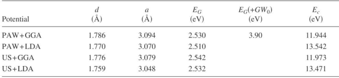
TABLE II. Si-C bond length d, lattice constant a, band gap EG, band gap corrected by GW0 EGW0, cohesive energy EC values for 2D monolayer of SiC in honeycomb structure calculated with different potentials. Potential d 共Å兲 a 共Å兲 EG 共eV兲 EG共+GW0兲 共eV兲 Ec 共eV兲 PAW+ GGA 1.786 3.094 2.530 3.90 11.944 PAW+ LDA 1.770 3.070 2.510 13.542 US+ GGA 1.776 3.079 2.542 11.973 US+ LDA 1.759 3.048 2.532 13.471
dimensionality. For example, the charge transfer calculated with Bader analysis increases with increasing dimensionality. While the energy band gap EGdoes not show a regular trend with dimensionality, the band gap of 2D monolayer is wider than those of 3D crystals.
V. BARE AND HYDROGEN PASSIVATED SIC NANORIBBONS
In this section, we consider bare and hydrogen passivated armchair SiC nanoribbons. These nanoribbons are specified according to their widths specified in terms of N number of Si-C basis in their unit cells. Hence, A-SiCNR共N兲 indicates armchair SiC nanoribbons having N Si-C pairs in their unit cell. We have analyzed A-SiCNR 共both bare and H-passivated兲 from N=5 to 21. A-SiCNR’s with odd num-bered N have reflection symmetry with respect to their axis. Bare armchair SiC nanoribbons are ferromagnetic in ideal honeycomb form. However, upon structural relaxation, re-construction occurs at the edges resulting in a considerable gain of energy and the structure becomes nonmagnetic.
Band gaps of all A-SiCNR共N兲 increase by ⬃0.7 eV upon H saturation of dangling bonds. The Si-H and C-H bonds formed after hydrogenation have lengths of 1.49 and 1.09 Å, respectively. The effective charges on Si and C edge atoms changes after H passivation. While Si-C bonds at the edges are shorter than the Si-C bonds in 2D SiC monolayer by 0.09 Å, upon H saturation these bonds get slightly longer, but are still shorter than the regular Si-C bonds by 0.05 Å. Hence, reconstruction of atomic structure at the edge exists in each case, but is more pronounced in the bare nanorib-bons.
Here we consider A-SiCNR共9兲 as a prototype and exam-ine its band structure. The bare A-SiCNR共9兲 is an indirect band gap semiconductor. Two bands at the conduction band edge are composed of edge states, which are split due to edge-edge interactions. These bands are removed upon H saturation of dangling bonds of atoms at the edges. This results in a widening of the band gap. As for the other edge state band, it is located in the valance band. This band is also removed upon H-saturation, but the valence band edge is not affected. The band gap of H-saturated A-SiCNR共9兲 is direct. Energy bands and band decomposed charge densities are shown in Fig. 4.
The variation of the energy band gap, EG, of bare and H-passivated SiC armchair nanoribbons with the width of the
ribbon N are calculated for 5ⱕNⱕ21 as presented in Fig.5. For bare A-SiCNR’s, the band gap is relatively smaller due to edge states as shown in Fig.4; namely, EG⬃1.29 eV for
N = 5, but increases to⬃2.4 eV for N=21. Upon H
passiva-tion of the dangling bonds at the edges, the edge states dis-appear and the band gap increases and gets direct. For N = 5 the direct band gap is around 2.5 eV, but increases with N and eventually becomes 2.38 eV for N = 21. Hypothetically, the band gap is expected to reach the value of 2D planar SiC 共EG= 2.53 eV calculated within GGA兲. The main difference with graphene is that the band gap of bare armchair graphene nanoribbon decreases with increasing N and eventually van-ish as N→⬁. Interestingly, H-saturated armchair SiCNRs with, N − 1, N, and N + 1, exhibit a family behavior similar to one revealed in armchair graphene nanoribbons.35 For N
⬎15 the variation of EGof H-saturated A-SiCNR is not sig-nificant. However, it should be noted that the band gap varia-tion of both bare and H-saturated armchair SiC nanoribbons cannot be reconciled with the quantum confinement effects, since EG increases with increasing N. This is due to other effects which overcome the quantum confinement effect. The variation in band gaps of bare and hydrogen passivated arm-TABLE III. Bonding types, Si-C distances d, lattice constants a, charge transfers␦q, effective charges on Si and C, respectively, ZSiⴱ and ZCⴱ, band gaps EGwith GW0corrections, and cohesive energies Ecfor comparison of SiC polymorphs.
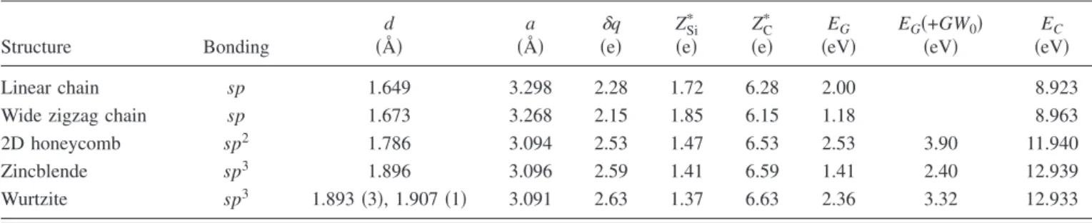
Structure Bonding d 共Å兲 a 共Å兲 ␦ q 共e兲 ZSiⴱ 共e兲 ZCⴱ 共e兲 EG 共eV兲 EG共+GW0兲 共eV兲 EC 共eV兲 Linear chain sp 1.649 3.298 2.28 1.72 6.28 2.00 8.923
Wide zigzag chain sp 1.673 3.268 2.15 1.85 6.15 1.18 8.963
2D honeycomb sp2 1.786 3.094 2.53 1.47 6.53 2.53 3.90 11.940
Zincblende sp3 1.896 3.096 2.59 1.41 6.59 1.41 2.40 12.939
Wurtzite sp3 1.893共3兲, 1.907 共1兲 3.091 2.63 1.37 6.63 2.36 3.32 12.933
FIG. 4. 共Color online兲 Energy band structure of the bare 共a兲 and hydrogen saturated 共b兲 armchair SiC nanoribbons, A-SiCNR共N兲 having 9 Si-C pairs共N=9兲 in the unit cell and isosurfaces of charge densities of selected states at the⌫-point of BZ. Zero of energy is set at the Fermi level. Energy band gap is shaded.
chair SiC ribbons are presented in Fig.5共c兲and5共d兲. In Ref. 31, the variation of the band gap with N and resulting family behavior is in agreement with present results. Whereas the same variation is not presented in Ref.31. The zigzag SiC-NRs exhibit interesting magnetic properties and were inves-tigated extensively by earlier works.31,36,37 For this reason,
the zigzag SiCNRs are examined in the present study.
VI. VACANCY DEFECTS AND ANTISITE
It has been shown that the vacancy defects have remark-able effects on 2D graphene honeycomb structure and its nanoribbons.38–43 Nonmagnetic graphene sheets or
nanorib-bons can attain spin polarized states due to vacancy defects. We expect that similar effects of vacancy defects can occur on the electronic and magnetic properties of SiC honeycomb structure.
A. 2D Honeycomb SiC
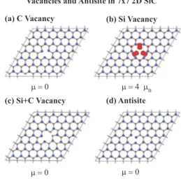
The effects of Si and C vacancies, Si+ C-divacancy and C-Si-antisite are treated in periodically repeating supercells. The size of supercell is optimized to allow negligible defect-defect interaction between adjacent cells. Here the width of the flat bands derived from the states of periodically repeat-ing vacancies is taken as the measure of the strength of vacancy-vacancy coupling. A共7⫻7兲 supercell is found to be suitable, since it leads to rather flat defect bands. At the same time it is not large and allows us to carry out numerical calculations within feasible computational time. The flat bands associated with vacancies can be considered as local-ized defect state 共if it is in the band gap兲 or resonance state
共if it is in the band continua兲. Here we consider localized defect states. Our results are presented in Fig.6for single C, Si vacancies, Si+ C divacancy, C + Si antisite defects.
A vacancy is generated first by removing a single atom, C or Si atom from each supercell of the monolayer of SiC as shown in Figs.6共a兲and6共b兲. Subsequently, the atomic struc-ture is optimized. Single C vacancy in 2D monolayer of SiC is nonmagnetic; Si atoms around vacancy with coordination number 2 are displaced in the transversal direction and do not induce any magnetic moment.
As for Si vacancy, three C atoms around vacancy re-mained planar. Similar to the vacancies in graphene and BN, Si-vacancy induces a local magnetization in the system. Is-ovalue surfaces of the difference between up and spin-down charge densities i.e.,⌬↑↓clearly shows a spin polar-ization around the vacancy and a net magnetic moment constructed there from. The calculated total magnetic mo-ment is 4B per supercell. The Si vacancy in a repeating 共7⫻7兲 give rise to defect states in the band gap. As for Si + C divacancy in Fig. 6共c兲, it is again nonmagnetic since the spins are paired; two C atoms around the vacancy choose to make a bond with each other. The band gap is also modified. Finally, we consider the antisite defect. The resulting relaxed structure is given in Fig. 6共d兲. Lattice is distorted as C-C bond is shorter than Si-Si bond in the antisite case. It is noted that the calculated magnetic moments for single Si and C vacancy do not agree with Lieb’s theorem,44which normally
predicts 1B net magnetic moment both for Si and C vacan-cies in Fig.6. We attribute the discrepancy between the re-sults of first principles calculations and Lieb’s theorem to the structural relaxation occurred after the generation of vacancy and significant charge transfer from Si to C. The localized electronic states associated with the vacancy defects and an-tisite are deduced from the band structure calculations as presented in TableIV, where the energies are given from the top of the valance band.
5 10 15 20 1.2 1.3 1.4 1.5 1.6 1.7 Bandgap (eV) Ribbon Width (N)
(a)
Unit Cell(b)
Unit CellN=9 N=9
(c)
(d)
Bar
e
H-pa
ssiva
ted
5 10 15 20 2.15 2.2 2.25 2.3 2.35 2.4 Bandgap (eV) Ribbon Width (N) FIG. 5. 共Color online兲 Optimized atomic structures for 共a兲 Bare 共b兲 H-passivated SiC nanoribbons. Large/blue and small/brown balls represent Si and C atoms, respectively. The variations of band gaps of 共c兲 Bare and 共d兲 H-passivated SiC nanoribbons with the ribbon width N for 5⬍N⬍21.(a) C Vacancy (b) Si Vacancy
(c) Si+C Vacancy (d) Antisite
µ = 0
µ = 0 µ = 0
µ = 4 µB
Vacancies and Antisite in 7x7 2D SiC
FIG. 6. 共Color online兲 Optimized atomic structure and magnetic moment of vacancy defects calculated in a共7⫻7兲 supercell of 2D SiC structure.共a兲 C vacancy; 共b兲 Si vacancy; 共c兲 C+Si divacancy; 共d兲 C-Si antisite. In 共b兲 the difference of spin-up and spin-down charges are shown. Large/blue and small/brown balls indicate Si and C atoms respectively.
B. Vacancy defects in SiC Nanoribbons
The effects of the vacancy defects on the electronic and magnetic properties are treated for of H-passivated A-SiCNR共9兲 using a 共4⫻1兲 repeating supercell. Our main motivation was to investigate what differences would occur in a ribbon. Optimized structures, calculated total magnetic moments are presented in Fig.7. Overall effects of vacancy, divacancy and antisite effects are similar to those in 2D SiC monolayer structure except in the antisite case the exchanged Si atom moves out of the plane about 0.9 Å. One localized state below the conduction band edge and one other state above the valence band edge occur due to antisite as donor and acceptor states, respectively.
VII. FUNCTIONALIZATION OF SIC HONEYCOMB STRUCTURE BY ADATOMS
Specific adatoms can bind to 2D SiC monolayer with sig-nificant binding energies. Adatom adsorption or decoration,
as well as substitution for Si or C atoms in the honeycomb structure by foreign atoms can modify the properties of 2D SiC monolayer and its nanoribbons. This way, SiC honey-comb structures can be functionalized. Adatom adsorption and substitution are considered within the periodically re-peating 共7⫻7兲 supercell geometry to minimize the interac-tion between them. The calculainterac-tions performed in a larger supercell共10⫻10兲 have also showed similar results which is an indication that the coupling between adjacent defects is negligible.
A. Adatom adsorption
As for adatom adsorption, we considered Al, Co, Fe, N, P, Ti by placing each of them on four different positions in the 共7⫻7兲 monolayer of SiC and then by fully relaxing the whole system. The initial positions of the adsorption are on top of silicon atom共TS兲, on top of carbon atom 共TC兲, at the center of hexagon 共HS兲, above the middle of the Si-C bond 共BS兲. The distance between adatoms is 12 Å. Spin polarized calculations are carried out to determine the binding struc-ture and binding energy. Whether the adatoms are bound to the surface are examined by calculating the binding energies of these six different individual atoms in terms of the calcu-lated total energies as EB= ET关SiC+adatom兴−ET关SiC共bare兲兴 − ET关adatom兴. We found that all of these adatoms are bound with a significant energy, which is larger than 1 eV. Flat bands indicate that states induced by the adatoms are rather localized and hence adatom-adatom interactions are negli-gible. Therefore, adatoms treated here in supercell geometry can represent single共isolated兲 adatom. Optimized adsorption sites, total magnetic moments, heights from the SiC plane are given in TableV.
B. Substitution of Si and C by foreign atoms
Here we examined the substitution of single Si or C atoms in 2D SiC honeycomb structure by various foreign atoms. Namely, B and N substituting C atom; Al, As, Ga, P substi-tuting Si atom. Similar to adatom calculations, the substitu-tion process is treated within periodically repeating 共7⫻7兲 supercell. Because of periodic boundary condition the local-ized states appear as flat bands. We found that B, N, As, and TABLE IV. Magnetic moments and positions of defect-induced state energies relative to the top of the
valance band. Spin-up共↑兲 and spin-down共↓兲 states are indicated. E 共F兲 indicate whether the defect state is empty共full-occupied兲.
Si+ C vacancy C-vacancy Si-vacancy Antisite
0 0 4B 0
E1共eV兲 0.49共F兲 0.15共F兲 0.09 共F↑兲 0.59共F兲
E2 1.40共E兲 1.82共E兲 0.11 共F↑兲 2.12共E兲
E3 2.45共E兲 1.95共E兲 0.31 共F↓兲
E4 0.33 共F↓兲
E5 0.38 共E↓兲
E6 1.47 共E↓兲
E7 1.49 共E↓兲
(a) C Vacancy (b) Si Vacancy
µ = 0 µ = 4 µB
(c) Si+C Divacancy (d) Antisite
µ = 0 µ = 0
Vacancy and Antisite in A-SiC NR (9)
FIG. 7. 共Color online兲 Magnetic moment of vacancy defects calculated in a共4⫻1兲 supercell of quasi 1D SiC armchair nanorib-bon with N = 9, i.e., A-SiCNR共9兲. Dangling bonds at both edges are saturated by hydrogen atoms. 共a兲 C vacancy; 共b兲 Si vacancy; 共c兲 Si+ C divacancy;共d兲 C-Si antisite. In 共b兲 the difference of spin-up and spin-down charges are shown while others are nonmagnetic. Large/blue and small/brown balls represent Si and C atoms respectively.
P atoms have a net magnetic moment= 1B. Ga and Al do not create any spin polarization. In Table VI, the substitu-tional impurity states in the band gap of 2D SiC and resulting net magnetic moments are given. The substitutional foreign atoms, namely B, N, As, and P have either 3 or 5 valence electrons and hence destroy the spin pairing in the perfect honeycomb structure. The substitution of C and Si by these atoms gives rise to a net magnetic moment of 1B. As a result, 2D SiC can be magnetized without doping by transi-tion metal elements.
VIII. DISCUSSION AND CONCLUSIONS
We present a study on 1D SiC chains, 2D monolayer of SiC in honeycomb structure and its armchair nanoribbons, 3D bulk SiC. We carried out stability analysis of those ma-terials. Two-dimensional monolayer of SiC is an ionic com-pound with charge transfer from silicon atoms to carbon at-oms and has a hexagonal lattice forming a planar honeycomb structure. The calculation of phonon modes results in all positive frequencies in BZ and indicates the stability of the planar honeycomb structure. This situation is in compliance with the previous works,16,32 where the honeycomb
struc-tures of binary compounds of group IV elements or III-V compounds are stable in planar geometry if they have an element from the first row, such as B, C, N. The 2D SiC is a
nonmagnetic wide band gap semiconductor. However, it ac-quires net magnetic moment when a single Si-vacancy defect is created or Si and C atoms of the honeycomb structure are substituted by As, P, B, and N. Single C-vacancy, Si+ C di-vacancy and Si-C antisite defects does not give rise to any magnetic moment in the system. It is shown that 2D SiC can be functionalized through Si-vacancy and adatom adsorption or substitution of Si C by foreign atoms.
Armchair SiC nanoribbons are found to be nonmagnetic semiconductors. We revealed the variation of band gap with the width of both bare and H-passivated nanoribbons. The variation of the band gap exhibits also family behavior. However, the band gaps of armchair nanoribbons are smaller than the band gap of 2D SiC for small N. Therefore the confinement effect seen in narrow graphene armchair nano-ribbons does not occur here.
In conclusion, our state-of-the-art first-principles calcula-tions demonstrate that 2D SiC monolayer is stable in honey-comb structure, and hence it has a strong chance to be syn-thesized in future. Above results indicate that bare and H-passivated SiC sheets and armchair nanoribbons can present interesting properties which can be utilized in nano-technology. Creating defects through vacancies, doping through adatoms and substitutional impurities can function-alize SiC honeycomb structure and hence add new magnetic and electronic properties.
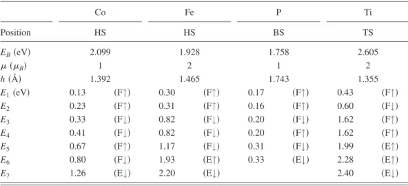
TABLE V. Binding energy EB, total magnetic moments, optimized heights of adatoms from the 2D monolayer of SiC h, and the energies of the localized states occurring in the band gap are given for each type of adatom. Empty共E兲, full 共F兲, spin-up and spin-down states are indicated. Energies of adatom induced localized states are given relative to the top of the valence band.
Co Fe P Ti Position HS HS BS TS EB共eV兲 2.099 1.928 1.758 2.605 共B兲 1 2 1 2 h共Å兲 1.392 1.465 1.743 1.355 E1共eV兲 0.13 共F↑兲 0.30 共F↑兲 0.17 共F↑兲 0.43 共F↑兲 E2 0.23 共F↑兲 0.31 共F↑兲 0.16 共F↑兲 0.60 共F↓兲 E3 0.33 共F↓兲 0.82 共F↓兲 0.20 共F↓兲 1.62 共F↑兲 E4 0.41 共F↓兲 0.82 共F↓兲 0.20 共F↑兲 1.62 共F↑兲 E5 0.67 共F↑兲 1.17 共F↓兲 0.31 共F↓兲 1.99 共E↑兲
E6 0.80 共F↓兲 1.93 共E↑兲 0.33 共E↓兲 2.28 共E↑兲
E7 1.26 共E↓兲 2.20 共E↓兲 2.40 共E↓兲
TABLE VI. Energies of defects states occurring in the band gap are given for each type of substituted atom. Empty共E兲, full 共F兲, spin-up and spin-down states are indicated. Energies are measured from the top of valence band.
B N As P
共B兲 1 1 1 1
E1共eV兲 0.23 共F,↑兲 1.47 共F,↑兲 0.75 共F,↑兲 1.18 共F,↑兲
ACKNOWLEDGMENTS
We would like to thank Dario Alfè for his valuable dis-cussions. Part of the computations has been carried out with
the service provided by UYBHM at Istanbul Technical Uni-versity through a Grant No. 2-024-2007. This work is par-tially supported by TUBA, Academy of Science of Turkey.
1Silicon Carbide: Recent Major Advances, edited by W. J. Choyke, H. Matsunami, and G. Pensl 共Springer-Verlag, Berlin, 2004兲.
2A. R. Lubinsky, D. E. Ellis, and G. S. Painter, Phys. Rev. B 11, 1537共1975兲.
3W. Y. Ching, Yong-Nian Xu, Paul Rulis, Lizhi Ouyang, Mater. Sci. Eng. 422, 147共2004兲.
4We. Zhou, L. Yan, Y. Wang, and Y. Zhang, Appl. Phys. Lett. 89, 013105共2006兲.
5A. Miranda, J. L. Cueva, A. E. Ramos, and M. Cruz-Irisson, Microelectron. J. 40, 796共2009兲.
6J. Q. Hu, Y. Bando, J. H. Zhan, and D. Golberg, Appl. Phys. Lett. 85, 2932共2004兲.
7K. J. Kim, S. Lee, J. H. Lee, M.-H. Roh, K.-Y. Lim, and Y.-W. Kim, J. Am. Ceram. Soc. 92, 424共2009兲.
8G. N. Yushin, Z. G. Cambaz, Y. Gogotsi, K. L. Vyshnyakova, and L. N. Pereselentseva, J. Am. Ceram. Soc. 91, 83共2008兲. 9W. Shan, A. J. Fischer, J. J. Song, G. E. Bulman, H. S. Kong, M.
T. Leonard, W. G. Perry, M. D. Bremser, and R. F. Davis, Appl. Phys. Lett. 69, 740共1996兲.
10S. F. Chichibu, M. Sugiyama, T. Kuroda, A. Tackeuchi, T. Kita-mura, H. Nakanishi, T. Sota, S. P. DenBaars, S. NakaKita-mura, S. P. DenBaars, and S. Nakamura, Appl. Phys. Lett. 79, 3600共2001兲. 11N. Camara, G. Rius, J.-R. Huntzinger, A. Tiberj, N. Mestres, P. Godignon, and J. Camassel, Appl. Phys. Lett. 93, 123503 共2008兲.
12J. Hou and B. Songa, J. Chem. Phys. 128, 154304共2008兲. 13K. S. Novoselov, A. K. Geim, S. V. Morozov, D. Jiang, Y.
Zhang, S. V. Dubonos, I. V. Grigorieva, and A. A. Firsov, Sci-ence 306, 666共2004兲.
14Y. Zhang, Y.-W. Tan, H. L. Stormer, and P. Kim, Nature 共Lon-don兲 438, 201 共2005兲.
15C. Berger, Z. Song, X. Li, X. Wu, N. Brown, C. Naud, D. Mayou, T. Li, J. Hass, A. N. Marchenkov, E. H. Conrad, P. N. First, and W. A. de Heer, Science 312, 1191共2006兲.
16S. Cahangirov, M. Topsakal, E. Akturk, H. Sahin, and S. Ciraci, Phys. Rev. Lett. 102, 236804共2009兲.
17P. E. Blöchl, Phys. Rev. B 50, 17953共1994兲.
18J. P. Perdew, J. A. Chevary, S. H. Vosko, K. A. Jackson, M. R. Pederson, D. J. Singh, and C. Fiolhais, Phys. Rev. B 46, 6671 共1992兲.
19G. Kresse and J. Hafner, Phys. Rev. B 47, 558共1993兲. 20G. Kresse and J. Furthmuller, Phys. Rev. B 54, 11169共1996兲. 21J. M. Soler, E. Artacho, J. D. Gale, A. Garcia, J. Junquera, P.
Ordejon, and D. Sanchez-Portal, J. Phys.: Condens. Matter 14,
2745共2002兲.
22D. Alfè, Comput. Phys. Commun. 180, 2622共2009兲. 23M. Shishkin and G. Kresse, Phys. Rev. B 74, 035101共2006兲. 24R. T. Senger, S. Tongay, E. Durgun, and S. Ciraci, Phys. Rev. B
72, 075419共2005兲.
25G. Henkelman, A. Arnaldsson, and H. Jonsson, Comput. Mater. Sci. 36, 354共2006兲.
26S. Tongay, E. Durgun, and S. Ciraci, Appl. Phys. Lett. 85, 6179 共2004兲.
27S. Tongay, R. T. Senger, S. Dag, and S. Ciraci, Phys. Rev. Lett.
93, 136404共2004兲.
28D. Bimberg, R. Blachnik, M. Carolone, P. J. Dean, Th. Grave, G. Harbeke, K. Hubner, U. Kaufmann, W. Kress, O. Madelung, W. von Munch, U. Rossler, J. Schneider, M. Schulz, and M. S. Skolnick, in Zahlenwerte und Funktionen aus Naturwissenschaft und Technik, Landolt-Bornstein, New Series, edited by O. Madelung, M. Schulz, and H. Weiss 共Springer-Verlag, Berlin, 1982兲 Group III, Pt. 17.
29J. Serrano, J. Strempfer, M. Cardona, M. Schwoerer-Bohning, H. Requardt, M. Lorenzen, B. Stojetz, P. Pavone, and W. J. Choyke, Appl. Phys. Lett. 80, 4360共2002兲.
30SiC Power Materials: Devices and Applications, edited by Zhe Chuan Feng共Springer-Verlag, Berlin, 2004兲.
31L. Sun, Y. Li, Z. Li, Q. Li, Z. Zhou, Z. Chen, J. Yang, and J. G. Hou, J. Chem. Phys. 129, 174114共2008兲.
32H. Şahin, S. Cahangirov, Topsakal M., E. Bekaroglu, E. Akturk, R. T. Senger, and S. Ciraci, Phys. Rev. B 80, 155453共2009兲. 33M. Topsakal and S. Ciraci, Phys. Rev. B 81, 024107共2010兲. 34M. Topsakal, S. Cahangirov, and S. Ciraci, arXiv:0908.2887
共un-published兲.
35Y.-W. Son, M. L. Cohen, and S. G. Louie, Phys. Rev. Lett. 97, 216803共2006兲.
36P. Lou and J. Y. Lee, J. Phys. Chem. C 113, 12637共2009兲. 37P. Lou and J. Y. Lee, J. Phys. Chem. C 113, 21213共2009兲. 38P. Esquinazi, D. Spemann, R. Höhne, A. Setzer, K.-H. Han, and
T. Butz, Phys. Rev. Lett. 91, 227201共2003兲.
39A. Hashimoto, K. Suenaga, A. Gloter, K. Urita, and S. Iijima, Nature共London兲 430, 870 共2004兲.
40O. V. Yazyev and L. Helm, Phys. Rev. B 75, 125408共2007兲. 41M. A. H. Vozmediano, M. P. Lopez-Sancho, T. Stauber, and F.
Guinea, Phys. Rev. B 72, 155121共2005兲.
42L. Brey, H. A. Fertig, and S. Das Sarma, Phys. Rev. Lett. 99, 116802共2007兲.
43M. Topsakal, E. Akturk, H. Sevinçli, and S. Ciraci, Phys. Rev. B
78, 235435共2008兲.