Experimental study of two-step growth of thin AlN film
on 4H-SiC substrate by Metalorganic Chemical Vapor
Deposition
H. YU*, M. OZTURK, P. DEMIREL, H. CAKMAK, T. BUYUKLIMANLIa, W. OUa, E. OZBAYb
Nanotechnology Research Center, Bilkent University, Bilkent, 06800 Ankara, Turkey
aEvans Analytical Group, East Windsor, NJ 08520
bNanotechnology Research Center, Department of Physics, and Department of Electrical and Electronics Engineering,
Bilkent University, Bilkent, 06800 Ankara, Turkey
We report growth optimizations of the thin AlN film on (0001) 4H-SiC substrates by metalorganic chemical vapor deposition. The influence of growth conditions, such as growth temperature and the V/III molar ratio, on the material quality of AlN film is studied. The surface morphology and crystalline quality of the epitaxial layers are investigated by atomic force microscope, X-ray diffraction, and transmission electronic microscope. A new approach is demonstrated to improve the crystalline quality of a 100 nm-thick AlN film by the use of a 5 nm-thick low temperature AlN nucleation layer. Compared to a conventional AlN layer directly grown on SiC substrate at high temperature, the surface morphology of two-step AlN film is remarkably improved along with a decreasing of defect density, leading to the improvement of crystalline quality for the subsequently grown GaN layer. The mechanisms of crystalline quality improvement by use of a low temperature AlN nucleation layer are also investigated and discussed.
(Received October 28, 2010; accepted November 25, 2010)
Keywords: AIN, Thin film, Metalorganic CVD
1. Introduction
AlGaN/GaN based high electron mobility transistors (HEMT) have offered great promise for high power, high voltage operations at microwave frequencies [1, 2]. Among the principle foreign substrates that are used for III-nitride epitaxy, SiC has remarkable advantages over sapphire and silicon for the development of high performance AlGaN/GaN HEMT device because of its high thermal conductivity, and reduced thermal and lattice mismatches with AlN (0.9%) and GaN (3.4%). A thin AlN film (∼ 100 nm) has been widely applied as a buffer layer on SiC in order to improve the crystal quality of the subsequent GaN by reducing the direct mismatch between GaN and SiC substrate, as well as for promoting the wetting of the substrate surface [3-6]. High crystalline quality AlN and GaN layers are desirable in AlGaN/GaN HEMT structure because the crystal defects can either cause a current collapse by deep trapping effects, or have negative effects on the interface roughness of the heterostructure. Moreover, it was reported that improvement of AlN quality can reduce the thermal resistance of AlGaN/GaN electronic device, i. e., temperature rise per input power density, which is responsible for an additional 30%–50% increase in device channel temperature in today’s AlGaN/GaN on SiC devices [7, 8]. Therefore, it provides a solution to improve the reliability of the AlGaN/GaN based HEMT devices by improving the thin AlN buffer quality. Furthermore, high
quality AlN also has potential to be used for optoelectronic devices. AlN based deep ultraviolet (~ 200 nm) light emitting diodes and photodetectors that are fabricated on SiC substrate have been demonstrated recently [9, 10].
Generally, the AlN buffer is grown directly on SiC at high temperature (>1100 °C) to enhance the surface motivation of the adatoms, and to achieve a single crystalline film, while a low growth temperature (<1050 ºC) leads to polycrystalline material [3]. The heteroepitaxy of high quality AlN is very difficult due to the poor motion of Al atoms on the growing surface, as well as the high bond energy of Al and N [11]. In order to obtain high quality AlN with an atomic smooth surface, high temperature (T>1400ºC) metalorganic chemical vapor deposition (MOCVD) growth is applied to enhance the Al atom diffusion length [12]. However, high temperature MOCVD system requires specialized heater and growth reactor designs. It is desirable to grow high quality AlN at a relatively low temperature which is compatible with the typical III-nitride MOCVD system by using novel growth schemes. These factors provide strong motivation to investigate the MOCVD growth conditions that lead to high crystalline quality thin AlN films that can consequently improve the crystal quality of GaN layer on it and the reliability and performance of electronic and optoelectronic devices on SiC substrate.
In the present study, we investigate the influence of growth conditions on the material quality of thin AlN film on SiC substrate. A two-step growth method is
demonstrated to improve the crystal quality of a thin AlN film. The mechanism of crystal quality improvement by using a low temperature AlN (LT-AlN) nucleation is also studied.
2. Experimental details
AlN films are grown on 4H–SiC (0001) substrates (Cree, Inc.) in a low-pressure horizontal MOCVD reactor (AIX 200/4 RF-S). Trimethylaluminum (TMAl) and ammonia were used as Al and N precursors, and H2 was
used as the carrier gas during AlN growth. Initially, the as-received SiC substrate is annealed at 1100 ºC for 10 min to remove surface contaminations, and no other treatment is carried out on the substrate. In order to investigate the influence of the growth temperature and V/III molar ratio on the material quality of an AlN film, two sets of samples were directly grown on SiC by using different V/III molar ratios of 230 and 7700 (named Set I and II), respectively. For both of two set samples, TMAl flow was kept as 8.2 μmol/min, and the V/III molar ratios were calibrated by varying the NH3 flow rates. The growth
temperature was changed in a range from 970 ºC to 1130 ºC, while other growth parameters were kept constant. The third set of the AlN (named Set III) was grown by employing a 5 nm-thick LT-AlN nucleation layer prior to high temperature growth. In the two-step growth, the LT-AlN nucleation was carried out in the region from 650 ºC to 950 ºC, and then the reactor temperature was ramped to 1130 ºC at a rate of 76 ºC/min. After that, the LT-AlN nucleation was annealed at 1130 ºC for 120 seconds, followed by high temperature AlN growth at this same temperature. All the AlN films have the same thickness of ~ 100 nm, which is the thickness that is normally used as a buffer layer for GaN and HEMT structure growth [4, 5, 13].
A high resolution X-ray diffractometer (Rigaku-Smartlab) was employed to examine the crystallite quality of the epitaxy AlN films, delivering a CuKa1 line of wavelength λ = 0.1541 nm. The atomic force microscopy (AFM), Veeco di-CP II, was used to evaluate the surface morphology of the as-grown AlN films by contact mode. Cross-sectional transmission electron microscopy (TEM) is performed by use of a Topcon 002B operating at 200 kV.
3. Results and discussion
The full width of half maximum (FWHM) of symmetric (0002) and asymmetric (10-15) X-ray rocking curves (XRCs) for the Set I and Set II as a function of growth temperature are shown in Fig. 1a and 1b, respectively. The FWHM of symmetric XRC for the epitaxy films with high density of defects, such as AlN on SiC substrate, is sensitive to the threading dislocations with screw component in the film, while the FWHM of asymmetric XRC is sensitive to all kinds of threading dislocations [14]. Obviously, the FWHMs of (0002) and (10-15) XRCs from both two sets show a similar tendency:
they decrease with the increase of the growth temperatures, similar to previous report [12]. It is because the high growth temperature helps to promote the surface migration of Al atoms and improve the AlN crystalline quality. Moreover, the FWHMs of both (0002) and (10-15) XRCs from the Set II are remarkably smaller than those from Set I, indicating a superior crystalline quality of the AlN films grown under a higher V/III molar ratio.
Fig. 1. FWHMs of the (0002) and (10-15) XRCs for 100 nm-thick AlN films grown directly on SiC at V/III molar ratio of 230 (a) and 7,700 (b), as a function of the growth temperature.
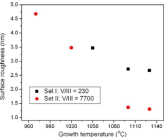
Fig. 2. RMS surface roughness of Set I and Set II AlN films as a function of the growth temperature.
The surface root mean square (RMS) roughness for Set I and Set II AlN films as a function of growth temperatures is summarized in Fig. 2. As shown in this figure, the AlN films grown under a higher V/III molar ratio exhibit a relatively low surface roughness compared to the samples grown with a low V/III molar ratio at the same growth temperature. At 1130 ºC, the RMS roughness was measured as 2.6 nm and 1.3 nm over a 2 × 2 µm2 area
for Set I and Set II, respectively. Moreover, the RMS roughness of the AlN films decreased remarkably with the increase of growth temperature for both of the two set samples. According to Fig. 1 and 2, our experiment results suggest that a relatively high growth temperature and a
high V/III molar ratio help to improve the crystalline quality, as well as AlN surface smoothness. It is easy to understand the effect of growth temperature on the quality of AlN film. High V/III ratio might decrease the interfacial energy and improve the wetting of the AlN on SiC.
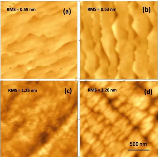
Fig. 3. 2 × 2 µm2 AFM images of 100 nm-thick AlN films grown directly on SiC under a V/III molar ratio of 7,700 at
970 ºC (a), 1020 ºC (b), 1100 ºC (c), and 1130 ºC (d).
AFM images of the Set II samples with a growth temperature from 970 ºC to 1130 ºC are shown in Fig. 3. On the surface of the AlN grown at 970 ºC (Fig. 3a), a high density of islands was found with random distributions. The RMS roughness was measured as 4.7 nm over a 2 × 2 µm2 area. When the growth temperature
increased to 1020 ºC, the island-like structure partially coalesces, as shown in Fig. 3b. When the growth temperature further increased to 1100 ºC and 1130 ºC, the island structure nearly coalesced fully but there is still high density of pits on the surface. The images showing coalesced process on the surface proved that higher growth temperature promotes the motion of Al atoms, in turn leading to improved crystalline quality. While for Set I, the AFM images (not shown here) exhibit that the three dimensional (3D) growth mode is kept during the growth
process with varied growth temperatures, and the surface roughness is not changed remarkably in our experiment temperature region due to the low V/III molar ratio.
To further improvement of the material quality of thin AlN film on SiC, a novel two-step growth was applied by using a 5 nm-thick LT-AlN nucleation. The growth process was optimized by calibrating the LT-AlN nucleation growth temperatures from 650 ºC to 950 ºC, while the other growth parameters were kept constant. As shown in Fig. 4, the surface morphology of AlN strongly depends on the LT-AlN nucleation temperatures. When the growth temperatures of LT-AlN nucleation are lower than 850 ºC, the surface of the 100 nm-thick AlN exhibits a pit-free fully coalesced surface and maintains a RMS roughness of < 1 nm, which is remarkably lower than that of Set I and Set II. In addition, for the AlN film with a 750
ºC nucleation layer, a smooth surface with well-developed step is observed throughout the scan area, indicating a step-flow growth mode. The surface RMS roughness is measured as 0.53 nm for a 2 × 2 µm2 scan area, as shown
in the inset of the image. The height difference between the two adjunct steps corresponds to two monolayers of the AlN along the (0001) direction. For the 750 ºC
nucleation sample, the FWHMs of AlN (0002) and (10-15) XRCs reach the value at 4.6 and 17.8 arcmin, respectively, which are also remarkably lower than those of Set I and Set II. The AFM images of sample with the 950 ºC nucleation layer tend to show a remarkably rougher
surface (RMS = 3.26 nm).
Fig. 4. 2 × 2 µm2 AFM images of 100 nm-thick AlN films grown on SiC with an LT-AlN nucleation layer deposited
at 650 ºC (a), 750 ºC (b), 850 ºC (c), and 950 ºC (d). Well-developed step flow growth with a pit-free surface was observed from the sample by using the LT-AlN nucleation layer deposited at 750 ºC.
To investigate the mechanism of the crystalline quality improvement by LT-AlN nucleation, AlN layers with thicknesses of 5 nm (the thickness as a nucleation layer) are grown on SiC at 1130 ºC and 750 ºC, respectively.
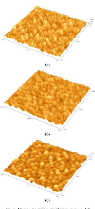
Fig. 5a and 5b show the three-dimensional (3D) AFM images of the two samples, which are measured over 1×1 µm2 scan area. A large number of randomly distributed 3D
nuclei configured with quite sharp tops can be seen on the surface of the two samples, indicating 3D initial growth mode in
(a)
(b)
(c)
Fig. 5. Microscopic surface morphology of 5 nm AlN layers on SiC (as measured by AFM with 1×1 µm2 scan
area) grown at (a) 1130 ºC, (b) 750 ºC, and (c) 750 ºC + annealing at 1130 ºC for 2 min.
spite of only a 0.9% lattice mismatch between AlN and SiC [11, 15]. However, clear differences are observed in Fig. 5a and 5b. In Fig. 5a, the average diameter (~ 50 nm) of AlN nuclei is approximately half the size of what (~ 100 nm) is shown in Fig. 5b. In addition, the root mean square (RMS) surface roughness over a 1×1 µm2 area is
measured as ~ 0.18 nm and ~ 0.12 nm for the sample grown at 1130 ºC and 750 ºC, respectively. At the initial stage of epitaxy growth, the texture development is controlled by the minimization of both film/substrate interfacial energy and film surface energy, which are
influenced by the epitaxy temperature. Our experimental results show that a lower growth temperature leads to larger nuclei and a relatively smoother surface, similar to previous reports [16, 17]. After in-situ annealing the LT-AlN nucleation at 1130 ºC for 2 min, the top of the LT-AlN nuclei become more rounded and some AlN nuclei are partially coalesced, as shown in Fig. 5c. It is due to the adatom motion at high temperature annealing process. Thin films grown on substrates with lattice mismatches usually exhibit a mosaic structure. In general, large grain size is desirable because the majority of dislocations in the epi-layer are formed at grain boundaries [18, 19]. Compared to AlN shown in Fig. 5a, Fig. 5c shows larger nuclei with smoother surface, which provide a better underlying seed layer for subsequent high temperature AlN growth.
(a)
(b)
Fig. 6. Cross-sectional TEM micrographs from AlN films on SiC substrate. The film that was grown by the one-step method shows high density of threading defects (a), whereas the film grown on an AlN nucleation layer (indicated in the picture) has a much lower defect density (b).
TEM is used to obtain detailed information on the configuration and the density of defects in samples with and without LT-AlN nucleation. TEM cross-sectional images of AlN film without and with 750oC nucleation are
shown in Fig. 6a and 6b, respectively, showing all types of dislocations. In Fig. 6a, the high density of dislocations and domain boundaries are observed to start from the AlN/SiC interface region, and most of them are all the way through the AlN epi-film. Moreover, the high density of V-shape pits with a depth about 5-10 nm are seen on the
top of the threading defects, as shown in Fig. 6a. Compared to Fig. 6a, the density of defects in Fig. 6b is remarkably reduced. The interface between 5 nm-thick LT-AlN nucleation and high temperature AlN can be clearly observed in that figure. This reduction in dislocations occurs at the top of nucleation layer, which are denoted by white arrows. The TEM characterizations provide direct evidence that LT-AlN nucleation layer plays a key role to reduce the defect density in the AlN film on SiC substrate.
Initially, AlN nuclei are formed on substrate, which subsequently coalesce to form larger grains and the threading dislocations get annihilated as the growth processes [20]. Finally, this results in the 2D step-flow growth for sample grown on 750 oC nucleation layer. For
sample without LT-AlN nucleation, the 3D mode growth is kept from the initial nuclei to about 100 nm due to the low surface lateral mobility of atoms, in which the grains do not coalesce fully. It is well known that the epitaxy of high quality AlN on foreign substrate is difficult due to the poor motion of Al atoms on the growing surface and the high bond energy of Al and N [21]. To achieve high quality AlN with an atomic smooth surface, the high temperature (T > 1400 ºC) MOCVD or pulsed mode (Al and N precursors are introduced into reactor separately) growth are applied to enhance the atom diffusion length [20, 22]. Normally, the thick epitaxial film is also needed to obtain high quality material, due to the long grain coalesce process by the poor growth rate along the lateral directions. In present research, we demonstrate that a LT-AlN nucleation and high temperature annealing process can supply a seeding layer with larger size of nuclei and smoother surface, which decrease the energy of Al atoms lateral motion, consequently promote the coalesce process and result in a low threading defect density.
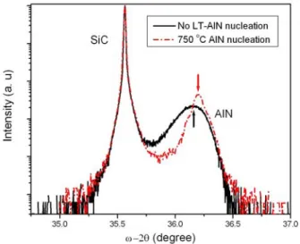
Fig. 7. (0002) ω-2θ of 100 nm-thick AlN films grown with and without a 750 ºC LT-AlN nucleation layer.
Fig. 7 shows the XRD (0002) ω-2θ scans of the AlN films with and without a 750 ºC LT-AlN nucleation layer. The dominant peaks in the figure are from the SiC
substrates. For the AlN peak of the film with a LT-AlN nucleation, it has significantly smaller FWHM and higher intensity, compared to that of the film without LT-AlN nucleation, indicating the improvement of crystalline quality. Moreover, it has a larger angular separation from the SiC peak than that of the film directly grown on SiC, indicative of a slightly smaller c lattice constant. This shows that the film with LT-AlN nucleation is under greater biaxial tension than the AlN directly grown on the SiC. According to the lattice and thermal mismatch, AlN grown on SiC should experiences about -1.0% biaxial compressive strain after the structure cooling down [22-24]. In contrast, the coalescence of masoic islands causes the biaxial tension strain in the film consisting of discrete grains, like AlN on SiC [25]. The LT-AlN nucleation can supply a seeding layer with larger size of nuclei and smoother surface, which can decrease the energy of Al atoms lateral motion, consequently promote the coalesce process and result in a fully coalesced step flow surface, as shown in Fig. 4. While the thin AlN films directly grown on SiC substrate (Set I) are not fully coalesced, and show the 3D rough surface. Therefore, the greater biaxial tension (smaller c lattice constant) in the AlN film with LT-AlN nucleation was attributed to an increased generation of grain coalesce tensional strain.
GaN films with a 2 μm thickness were grown by using identical growth conditions on these two kinds of AlN buffer [26]. As was expected, for the GaN grown on two-step AlN buffer, the full width at half maximum (FWHM) of the XRD rocking curve was measured as 124 arcsec for (0002) and 316 arcsec for (10-12) reflections, respectively. Whereas for the sample grown on one-step AlN buffer, it showed 276 arcsec for (0002) and 433 arcsec for (10-12) reflections, respectively. The higher crystal quality for the GaN layer by using an improved quality two-step AlN buffer layer was confirmed by the lower XRD FWHMs on both the symmetric and asymmetric reflections.
In summary, we investigate the MOCVD growth and material characteristics of thin AlN layers on 4H-SiC substrates. The influence of growth conditions, such as growth temperature and the V/III molar ratio on the material quality of AlN film, was studied. The two-step growth method was applied to grow high quality AlN film by using a thin LT-AlN nucleation layer. After high temperature annealing, LT deposited AlN nuclei show a configuration of a larger size grain and smoother surface, compared to the sample that was directly grown on SiC at high temperature. For the 100 nm AlN film, the two-step grown sample exhibited well-developed parallel atomic steps, indicating a step flow growth mode and reduced dislocation density, which is confirmed by XRC and cross-sectional TEM. The mechanisms of crystal quality improvement by using a LT-AlN nucleation layer were also discussed.
Acknowledgement
This work is supported by the European Union under the projects EU-PHOME, and EU-CONAM, and
TUBITAK under Project Nos., 107A004, and 107A012. One of the authors (E. O.) also acknowledges partial support from the Turkish Academy of Sciences.
Reference
[1] M. A. Khan, A. Bhattarai, J. N. Kuznia, D. T. Olson, Appl. Phys. Lett., 63, 1214 (1993).
[2] Y.-F. Wu, A. Saxler, M. Moore, R. P. Smith, S. Sheppard, P. M. Chavarkar, T. Wisleder, U. K. Mishra, P. Parikh, IEEE Electron Device Lett. 25, 117 (2004).
[3] T. Warren Weeks, Jr., Michael D. Bremser, K. Shawn Ailey, Eric Carlson, William G. Perry, Robert F. Davis, Appl. Phys. Lett. 67, 401 (1995).
[4] D. D. Koleske, R. L. Henry, M. E. Twigg,
J. C. Culbertson, S. C. Binari, A. E. Wickenden, M. Fatemi, Appl. Phys. Lett. 80, 4372 (2002).
[5] Y. N. Picard,M. E. Twigg, M. A. Mastro, C. R. Eddy, Jr., R. L. Henry, R. T. Holm, P. G. Neudeck,
A. J. Trunek, J. A. Powell, Appl. Phys. Lett. 91, 014101 (2007).
[6] P. Waltereit, O. Brandt, A. Trampert, M. Ramsteiner, M. Reiche, M. Qi, K. H. Ploog, Appl. Phys. Lett. 74, 3660 (1999).
[7] A. Sarua, H. Ji, K. P. Hilton, D. J. Wallis, M. J. Uren, T. Martin, M. Kuball, IEEE Trans. Electron Devices, 54, 3152 (2007).
[8] G. Riedel, J. Pomeroy, K. Hilton, J. Maclean, D. Wallis, M. Uren, T. Martin, U. Forsberg, A. Lundskog, A. Georgieva, G. Pozina, E. Janzén, R. Lossy, R. Pazirandeh, F. Brunner, J. Würfl, M. Kuball, IEEE Electron Device Lett. 30, 117 (2004).
[9] Y. Taniyasu, M. Kasu, T. Makimoto, Nature (London) 441, 325 (2006).
[10] R. Dahal, T. M. Al Tahtamouni, Z. Y. Fan, J. Y. Lin, H. X. Jiang, Appl. Phys. Lett. 90, 263505 (2007). [11] A. Costales, M. A. Blanco, A. M. Pendas,
A. K. Kandalam, R. Pandey, J. AM. CHEM. SOC, 124. 4117 (2002).
[12] M. Imura, H. Sugimura, N. Okada, M. Iwaya, S. Kamiyama, H. Amano, I. Akasaki, A. Bandoh, Journal of Crystal Growth. 310, 2308 (2008).
[13] W. Saito, Y. Takada, M. Kuraguchi, K. Tsuda, I. Omura, T. Ogura, and H. Ohashi, IEEE
Transactions On Electron Devices 50, 2528 (2003). [14] B. Heying, X. H. Wu, S. Keller, Y. Li, D. Kapolnek, B. P. Keller, S. P. DenBaars, J. S. Speck, Appl. Phys. Lett. 68, 643 (1996).
[15] S. Yamada, J. Kato, S. Tanaka, I. Suemune, A. Avramescu, Y. Aoyagi, N. Teraguchi, A. Suzuki, Appl. Phys. Lett. 78, 3612 (2001).
[16] M. H. Kim, M. Oshima, H. Kinoshita, Y. Shirakura, K. Miyamura, J. Ohta, A. Kobayashi, H. Fujioka, Appl. Phys. Lett. 89, 031916 (2006).
[17] M. Kim, J. Ohta, A. Kobayashi, H. Fujioka, M. Oshima, phys. stat. sol. (RRL) 2, 13 (2008). [18] F.A. Ponce, B.S. Krusor, J.S. Major Jr.,W. E. Plano, D. F. Welch, Appl. Phys. Lett. 67, 410 (1995). [19] A. E. Wickenden, D. D. Koleske, R. L. Henry, R. J. Gorman, J. C. Culbertson, M. E. Twigg, J. Electron. Mater. 28, 301 (1999).
[20] M. Imura, K. Nakano, N. Fujimoto, N. Okada, K. Balakrishnan, M. Iwaya, S. Kamiyama, H. Amano, I. Akasaki, T. Noro, T. Takagi, A. Bandoh, Jpn. J. Appl. Phys. 45, 8639 (2006).
[21] A. Costales, M. A. Blanco, A. M. Pendas,
A. K. Kandalam, R. Pandey, J. AM. CHEM. SOC.
124, 4117 (2002).
[22] Z. Chen,S. Newman, D. Brown, R. Chung, S. Keller, U. K. Mishra, S. P. Denbaars, S. Nakamura, Appl. Phys. Lett. 93, 191906 (2008).
[23] W. M. Yim, R. J. Paff, J. Appl. Phys. 45, 1456 (1974). [24] J. R. OConner, J. Smiltens, Silicon Carbide (New York, Pergamon, 1960).
[25] M. Asif Khan, M. Shatalov, H. P. Maruska, H. M. Wang, E. Kuokstis, Jpn. J. Appl. Phys., 44 7191 (2005).
[26] H. Yu, M. K. Ozturk, S. Ozcelik, E. Ozbay, Journal of Crystal Growth. 293, 273 (2006).
________________________
*Corresponding author: [email protected],