phys. stat. sol. (c) 4, No. 2, 288– 291 (2007) / DOI 10.1002/pssc.200673233
© 2007 WILEY-VCH Verlag GmbH & Co. KGaA, Weinheim
Raman and TEM studies of Ge nanocrystal formation in
SiO
x:Ge/SiO
xmultilayers
A. Dana*, 1, S. Ağan2, S. Tokay2, A. Aydınlı1, and T. G. Finstad3
1 Physics Department and National Nanotechnology Research Center, Bilkent University, 06800 Ankara, Turkey
2 Physics Department, Kırıkkale University, 71450 Kırıkkale,Turkey
3 Physics Department, University of Oslo, P.O. Box 1048 - Blindern, 0316 Oslo, Norway
Received 30 July 2006, revised 3 September 2006, accepted 3 September 2006 Published online 7 February 2007
PACS 68.37.Lp, 68.65.-k, 81.07.Bc, 81.15.Gh, 81.40.Ef
Alternating germanosilicate-siliconoxide layers of 10-30 nm thickness were grown on Si substrates by plasma enhanced chemically vapor deposition (PECVD). The compositions of the grown films were de-termined by X-ray photoelectron spectroscopy measurements. The films were annealed at temperatures varying from 670 to 1000 °C for 5 to 45 minutes under nitrogen atmosphere. High resolution cross section TEM images, electron diffraction and electron energy-loss spectroscopy as well as energy-dispersive X-ray analysis (EDAX) data confirm presence of Ge nanocrystals in each layer. The effect of annealing on the Ge nanocrystal formation in multilayers was investigated by Raman spectroscopy and Transmission Electron Microscopy (TEM). As the annealing temperature is raised to 850 °C, single layer of Ge nanocrystals observed at lower annealing temperatures is transformed into a double layer with the smaller sized nanocrystals closer to the substrate SiO2 interface.
© 2007 WILEY-VCH Verlag GmbH & Co. KGaA, Weinheim
1 Introduction The possible use of semiconductor nanocrystals for applications in electronic and optical devices has provided strong motivation for research in this field. Despite the indirect band gaps associated with bulk silicon and germanium inhibiting light emission, both quantum confinement effects and their compatibility with current Si based microelectronics process technology makes Si and Ge nanocrystals even more attractive. Many research groups have studied the formation and subsequent optical and electrical properties of Si and Ge nanocrystals [1]. Among many properties of interest, struc-tural information revealing crystal structure, nanocrystal shape, type and density defects is fundamental because they determine almost all other properties of the nanocrystals. Structural information can be obtained by several analytical techniques such as X-ray diffraction (XRD), transmission electron micros-copy (TEM) and Raman scattering spectrosmicros-copy to name a few [2, 3]. Ge nanocrystals have been ob-tained by ion beam synthesis in SiO2 and post growth annealing [4, 5]. TEM characterization showed Ge nanocrystals with a mean diameter of few nm’s depending on implantation dose and annealing time and temperature.
In this work, we report on formation of Ge nanocrystals in multilayered grown with plasma enhanced chemical vapor deposition (PECVD). We used both high resolution TEM and Raman scattering spec-troscopy to determine size and crystallinity of Ge nanocrystals. The size dependent spatial separation of Ge nanocrystals has been observed. This may be crucial for memory device applications. PECVD allows for the control of the thickness of the SiO2 tunnel oxide underneath the nanocrystal layer, as well as the density and size of the Ge nanocrystals.
phys. stat. sol. (c) 4, No. 2 (2007) 289
www.pss-c.com © 2007 WILEY-VCH Verlag GmbH & Co. KGaA, Weinheim 2 Experimental procedure The oxide (10 nm)-germanosilicate (10-30 nm) - oxide (50 nm) multi-layered films were grown in a PECVD reactor (model PlasmaLab 8510C) on Si substrates using 180 sccm SiH4 (2% in N2), 225 sccm N2O and varying flow rates of GeH4 (2% in He) as precursor gases, at a sample temperature of 350 °C, a process pressure of 1000 mTorr under and an applied RF power of 10 W. First, a tunnel oxide followed by a deposition of a SiOx:Ge layer and a layer of SiOx was grown. SiOx:Ge and SiOx layers form a pair. Samples with layers ranging from 3 to 10 pairs have been grown. Germanium doped SiOx:Ge layer is where nanocrystals form upon annealing. The samples were then annealed in N2 atmosphere in a quartz oven at temperatures ranging from 670 to 1000 °C for 5 to 45 minutes. The structural characterization was carried out in a 200 kV JEOL 2010F field-emission TEM located at University of Oslo, making use of diffraction, tilt and rotation facilities.
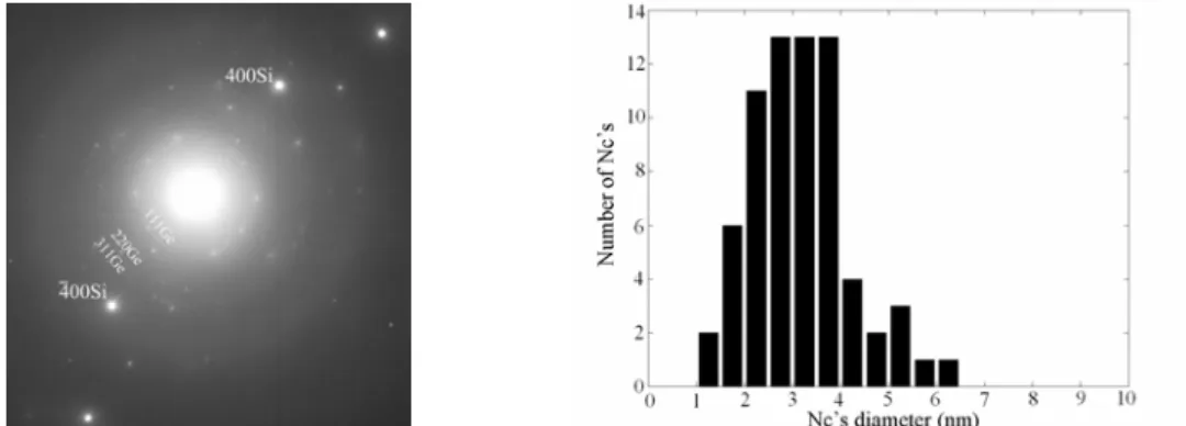
3 Results and discussion The samples were grown as alternating layers of germanosilicate and sili-con oxide using PECVD. Deposited layers are prepared by varying the flux ratios of SiH4 (2% in N2) and GeH4 (2% in He), systematically. These have been heat treated at different temperatures 670 to 900 °C for 5 to 45 min. Cross-sectional TEM image in Fig. 1 shows 3 germanosilicate layers with nanocrys-tal formation annealed at 900 °C for 45 min. First layer consists of 12 nm thick germanosilicate and the others are 30 nm thick with 50 nm SiO2 spacer layer in between. We observe small Ge nanocrystals in the first germanosilicate layer at the SiO2/Si interface while Ge nanocrystals in the second and third layers are larger. Smaller nanocrystals are due to limited amount of Ge in the thinner first germanosili-cate layer. Based on HRTEM images of these samples, Ge nanocrystal sizes range 7-30 nm. The micro-graph shows perfect alignment of crystallomicro-graphic planes in the Ge nanocrystals that have clearly pro-nounced facets. From the figures, different nanocrystals show different orientations of crystallographic planes. We see the formation of Ge nanocrystals in each layer of the multilayer sample. Ge particles were analyzed with selected area diffraction (SAD). Figure 2(a) shows a typical diffraction pattern with rings indicating randomly oriented diamond Ge crystals. Table 1 summarizes average lattice parameters. The particle sizes increase as function of annealing temperature. Figure 2(b) shows nanoparticle size distribution in the layers with the largest Ge concentration and annealing at 770 °C for 5 min.
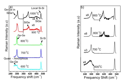
Figure 3 displays the results of Raman measurements from the same samples displaying the evolution of Ge nanocrystal formation upon annealing at temperatures in the range of 600-900 °C. As an example, we show the spectra for samples in the annealing temperature ranges 600 to 1000 °C for 45 min. (Fig. 3(a)). The spectrum remains unchanged for the annealing temperatures less than 600 °C. We observe a very broad (~40 cm–1) asymmetric peak centered around 291 cm–1 indicative of the quasi amorphous nature of the Ge for samples annealed at 600 °C. Si substrate is observed at 520.4 cm–1. If the annealing tempera-ture is raised to 700 °C, a sharp peak at 299 cm–1, now 10 cm–1 in width, is accompanied by a wide shoulder on the low frequency side. The sharp peak is a clear sign of Ge nanocrystal formation accompa-nied by a range of smaller Ge nanostructures. We note that this peak is at a lower frequency than the Ge mode in bulk Ge. This is due to phonon confinement in small crystals [6]. This peak becomes stronger and narrower (8 cm–1) and the broad quasi amorphous structure becomes weaker as the annealing tem-perature is increased up to 800 °C. At this temperature, in addition to the features associated with Ge nanocrystals, the spectrum now displays a weak but clearly discernible asymmetric peak centered at 419.5 cm–1 indicating the formation of SiGe alloy at the oxide Si substrate interface. In fact, if the oxide layer is completely removed with dilute HF solution, the same board peak at 419.5 cm–1 is still observ-able. Furthermore, remnants of the quasi amorphous feature completely disappear in favor of an asym-metric Ge mode which now shifts to 304 cm–1. The linewidth of the Ge mode increases dramatically when the sample is annealed at 900 °C. The SiGe alloy peak is stronger at 413 cm–1, also asymmetric on the low frequency side. Finally, the Si substrate peak observed as a sharp peak centered about 520.5 cm–1 is accompanied by a broad shoulder on the low frequency side centered around 499 cm–1. This is Si-Si appearing due to further interdiffusion of Si and Ge at the interface. With increasing annealing tempera-ture, these peaks behaved differently. A strong Si optic mode from the substrate is observed at 520 cm–1. The annealing temperature dependence of the Raman spectrum depends on the Ge concentration in films.
290 A. Dana et al.: Raman and TEM studies of Ge nanocrystal formation in SiOx:Ge/SiOx multilayers
© 2007 WILEY-VCH Verlag GmbH & Co. KGaA, Weinheim www.pss-c.com
We found that as the Ge concentration decreases, annealing at a higher temperature is necessary to obtain samples showing the sharp Ge mode in the Raman spectrum.
4 Conclusions We have shown the formation of crystalline Ge nanocrystals in SiO2 matrices grown with PECVD technique by using HRTEM, EDAX, Raman scattering and electron diffraction. Each layer in the multilayer of SiOx:Ge/SiOx system contains Ge nanocrystals. The mean size of the Ge nanocrystals was found to be between 7 and 30 nm depending on the annealing temperature and duration. With in-creasing annealing temperatures, defect densities decrease and crystal sizes increase.
Raman scattering was used to monitor the formation of Ge nanocrystals for nitrogen annealed samples. We have demonstrated that in many Raman scattering studies of Ge nanocrystals prolonged annealing results in the formation of SiGe alloy at the oxide Si interface. This also results in the detoriation of the Ge nanocrystals in the oxide layers.
Table 1 Measured size of Ge (diamond structure) unit cell.
Spec. annealing temp. / 0C cell dimension / Å
660 5.7 0.2±
770 5.63 0.06±
850 5.57 0.06±
Fig. 1 Cross-sectional TEM micrograph of multilayered sample, grown with 90 sccm of germane flow rate annealed at 900 °C for 45 min exhibiting Ge nanocrystal bands.
Fig. 2 (a)Typical diffraction pattern for a sample with Ge nanocrystals; (b) shows nanoparticle size distribution in the layers with largest Ge concentration for the 770 °C annealing for 300 sec.
phys. stat. sol. (c) 4, No. 2 (2007) 291
www.pss-c.com © 2007 WILEY-VCH Verlag GmbH & Co. KGaA, Weinheim Fig. 3 Raman spectra from SiOx: Ge films with 120 sccm (Si1.0Ge0.67O3.6) (a) and 90 sccm (Si1.0Ge0.54O3.4) (b) gas flow rate at different annealing temperatures for 45 min.
Acknowledgements This work is a supported by European FP6 project SEMINANO with the contract number 505285 and by TUBİTAK under contract TBAG-U/85(103T115). We gratefully acknowledge Prof. Ş. Süzer of Bilkent University, Chemistry Department for the XPS measurements.
References
[1] C. Bonafos, B. Garrido, M. Lopez, A. Perez-Rodriguez, J. R. Morante, Y. Kihn, G. Ben Assayag, and A. Clav-erie, Appl. Phys. Lett. 76, 3962 (2000).
[2] A. Karmous, I. Berbezier, and A. Ronda, Phys. Rev. B 75, 75323 (2006).
[3] U. Serincan, G. Kartopu, A. Guenness, T. G. Finstad, R. Turan, Y. Ekinci, and S. C. Bayliss, Semicond. Sci. Technol. 19, 247 (2004).
[4] R. J. Walters, G. I. Bourianoff, and H. A. Atwater, Nature Mater. 4, 143 (2005).
[5] W. K. Choi, V. Ho, V. Ng, Y. W. Ho, S. P. Ng, and W. K. Chim, Appl. Phys. Lett. 86, 143114 (2005). [6] Y. Maeda, Phys. Rev. B 51, 1658 (1995).
240 300 360 420 480 540 Frequency Shift (cm-1) x8 6000 C x3 700 0 C 800 0 C x8 x8 Ram an I nt ensi ty (a. u) 900 0C b) 240 300 360 420 480 540 600 0 C Frequency shift (cm-1) Ge-Ge in SiGe 700 0C SiGe x8 900 0C Quasi - Amorphous Ge-Ge a) 1000 0C x4
Raman Intensity (a.u)
800 0 C Ge-Ge Si-Si Local Si-Si SiGe