Electrical Size Reduction of Microstrip
Antennas by Using Defected Ground Structures
Composed of Complementary Split Ring
Resonator
Elif M. Kucukoner1,2, Alparslan Cinar2,3, Umut Kose2,4, and Evren Ekmekci1,2 1 Department of Electrical and Electronics Engineering, Suleyman Demirel University, 32260, Isparta, Turkey 2 Department of Electronics and Communication Engineering, Suleyman Demirel University, 32260, Isparta, Turkey 3 Elmali Vocational School, Akdeniz University, 07700, Antalya, Turkey
4 Department of Electrical and Electronics Engineering, Fatih Sultan Mehmet Vakif University, 34445, Istanbul, Turkey
Corresponding author: E. Ekmekci (e-mail: [email protected]).
ABSTRACT In this study the effects of using defected ground structures (DGS) composed of a complementary split ring resonator (CSRR) and CSRR with dumbbell (CSRR-D) for rectangular microstrip antennas are investigated. On this aim, two different antennas, which are Antenna B having CSRR etched DGS and Antenna C having CSRR-D etched DGS are designed and fabricated in comparison with the ordinary rectangular patch antenna, which is Antenna A. In both Antenna B and C, CSRR structures are etched in the same position of the ground planes. On the other hand, another ordinary microstrip antenna, called Antenna D, is designed at resonance frequency of Antenna C. For the characterization, resonance frequencies, voltage standing wave ratios, percentage bandwidths, gains, ka values and gain radiation patterns are investigated both in simulations and experiments. The numerical analyses show that 29.39 % and 44.49 % electrical size reduction (ESR) ratios are obtained for Antenna B and Antenna C, respectively in comparison to Antenna A. The experimental results verify the ESR ratios with 29.15 % and 44.94 %. Supporting, Antenna C promises 68.12 % physical size reduction (PSR) as it is compared with Antenna D. These results reveal that Antenna C is a good alternative for DGS based microstrip electrically small antennas.
INDEX TERMS Complementary split ring resonator, defected ground structure, electrical size reduction, microstrip patch antenna, miniature antenna.
I. INTRODUCTION
ECENTLY together with the increasing demand for mobile communication systems, designing planar small antennas have become important and popular [1-55]. In literature, the common methods of electrical size reduction (ESR) are using a substrate material with a high dielectric constant [1], using inductive and dielectric loadings [2,3,54], using magneto-dielectric materials [4,55], using metamaterial-based structures [5-9,55], using shorting pins [2,10,54] and finally using defected ground structures (DGSs) [11-36, 44-53].
In this study, ESR of microstrip antennas are studied by using CSRR based DGSs. On this aim, four different microstrip antennas are designed, fabricated, and characterized. The first antenna, which is Antenna A, is an ordinary rectangular patch antenna with 2.45 GHz resonance frequency in simulation. The second one, which is Antenna B, is the rectangular patch antenna having the DGS which is composed of a rectangular shaped CSRR. Following the third
one, which is Antenna C, is the rectangular patch antenna having the DGS composed of a modified CSRR i.e., CSRR-D, and finally the fourth one is, which is Antenna CSRR-D, an ordinary rectangular patch antenna whose resonance frequency is the same with Antenna C in simulation. Antenna A and Antenna D have entire copper sheets as the ground plane. On the other hand, in both Antenna B and C, CSRR structures are etched in the same position of the ground planes. It is important to note that a very similar topology to Antenna B has been studied by Rajeshkumar and Raghavan (2013) to provide a dual band of operation and electrical size reduction. In the topology, different than Antenna B, the gap of the CSRR is directed upwards [27]. Although there is a similar topology in the literature, the presentation of Antenna B in this study is important, since it forms the starting point of the proposed Antenna C and make it possible to reveal the improvements come from Antenna C in a fair comparison.
For the characterization of the antennas, resonance frequencies (f0), voltage standing wave ratios (VSWR),
E. M. Kucukoner et al.
percentage bandwidths (% BW), ka values (i.e., a figure of merit for the electrical size of an antenna), % ESR rations, gain values (G) and gain radiation patterns are investigated both in simulations and experiments. Besides radiation efficiencies (ecd) and directivities (D) are investigated
numerically. II. DESIGN
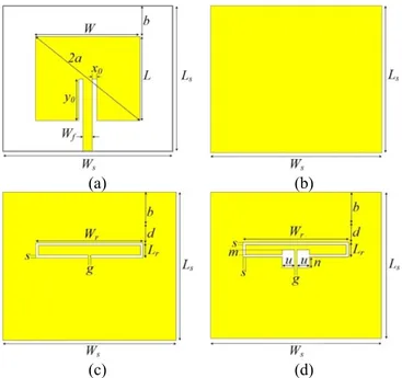
The schematic views of the antenna structures and their design parameters are illustrated in Fig. 1. In more detail, Fig. 1(a) represents the top views of all antennas. On the other hand, Fig. 1(b) represents the bottom views (i.e., ground planes) of the antennas A and D, Fig. 1(c) represents the ground plane for Antenna B and finally Fig. 1(d) shows the ground plane for Antenna C. All the antennas are designed by using Ws × Ls sized Arlon AD300A laminates,
which have 1.524 mm-thick-dielectric layers (i.e., h = 1.524 mm) with dielectric constant ε!= 3 and dielectric loss tangent tanδ = 0.002 at 10 GHz sandwiched by 0.035 mm-thick-copper layers (i.e., t = 0.035 mm, 𝜎"#= 5.8 × 10$ S/m). A W × L sized metallic patch is placed at the center of the top layer as shown in Fig. 1(a). The distance of the upper edge of the patch from the upper edge of the substrate is defined by parameter b. The patch is fed by 50 Ω microstrip line having line width Wf. An inset cavity is applied at the
feeding point for impedance matching between the antenna and the transmission line [27]. The width and length of the inset cavity are represented by x0 and y0, respectively. It is
important to note here that depending on the positions of CSRR-D and CSRR on the ground plane, i.e., depending on the parameter d in Fig. 1(d), the input impedance of the antenna changes and hence, this results with a change in y0 in
each design. For Antenna B and C, the DGS consists of a Wr
× Lr sized CSRR structures having groove width s and gap
width g. Herein, the projection lines of the upper edges of the patches are separated with the resonators by the distance d. For Antenna C a few additional parameters are also needed to be defined, which are dumbbell width u, dumbbell inner length m and dumbbell outer length n as shown in in Fig. 1(c) and (d). The values of the design parameters were decided in house based on a series of detailed parametric analyses in simulations. During the simulations, the dimensions of the CSRR based resonators were limited in the projection area of the rectangular patch to avoid an increase in the overall structures’ electrical size due to the additional CSRR. Moreover, the values of the design parameters were determined to achieve a higher gain and in the meanwhile a better ESR. On this purpose u, m, and n parameters, which came together with the proposal of Antenna C, provided an important flexibility and improvement. As the output, some pioneering numerical studies were presented in a national conference [19]. In this study, the design given in reference [19] is examined in more detail considering further numerical analyses, fabrication, and experimental studies. This examination is performed in a comparative manner firstly
with the Antennas A, B and D and secondly with the related literature. All the final design parameters and their values are tabulated in Table I including their explanations.
(a) (b)
(c) (d)
FIGURE 1. Schematic views of the antenna structures and the design
parameters. (a) Top view. (b) Bottom view for Antenna A and D. (c) Bottom view for Antenna B. (d) Bottom view for Antenna C.
TABLEI.Antenna design parameters
Parameter Valid for Quantity Value (mm)
Ws Ant A, B, C width of the substrate 70
Ant D 121
Ls Ant. A, B, C length of the substrate 60
Ant. D 107
W Ant. A, B, C Ant. D width of the metallic patch 43.29 75 L Ant. A, B, C Ant. D length of the metallic patch 34.8 63
Wf All width of the feed 3.79
a Ant. A, B, C Ant. D half of maximum linear dimension of the patch 27.771 48.974 x0 All width of the inset cavity 1.895
y0
Antenna A
length of the inset cavity
11.10
Antenna B 13.3
Antenna C 17.15
Antenna D 20.75
Wr Antenna B Antenna C width of the DGS 43.29
Lr Antenna B Antenna C length of the DGS 6
s Antenna B Antenna C line width of DGS 1
g Antenna B Antenna C gap width of DGS 1
m Antenna C dumbbell inner length 2
n Antenna C dumbbell outer length 4.5
u Antenna C dumbbell width 5
b Ant. A, B, C Ant. D distance from antenna to substrates top edge 12.6 22 d Antenna B Antenna C to antennas top edge distance from DGS 8
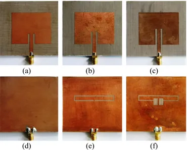
For the experimental purposes, the designed antennas are fabricated, and the photographs of Antenna A, B and C are shown in Fig. 2 including their top and bottom views. Besides, the top view of the fabricated Antenna D is presented in Fig. 3 in comparison to that of Antenna C to reveal the PSR. For all antennas, SMA type connectors with 50 Ω characteristic impedances are mounted at the transmission line ends.
(a) (b) (c)
(d) (e) (f)
FIGURE 2. The photographs of the fabricated antenna structures. (a)
Antenna A. (b) Antenna B. (c) Antenna C. (d) Antenna A ground plane. (e) Antenna B DGS. (f) Antenna C DGS.
FIGURE 3. Photographs of Antenna C and Antenna D.
III. SIMULATIONS and EXPERIMENTS
In this study, the antenna structures are numerically characterized by CST Studio Suite®. During the simulations, frequency domain solver is used since the structures have a resonant behavior. The antenna structures are excited by waveguide ports and the computational domain is finalized by open-add boundaries. The simulation outputs are |𝑆%%|, radiation efficiency ecd, directivity D, gain G and the
radiation pattern in terms of gain with respect to elevation angle. On the other hand, |𝑆%%| measurements in the experiments are carried out by using Agilent Fieldfox N9926A vector network analyzer. Finally, the gain and the radiation pattern measurements are taken in the anechoic chamber facility of Department of Electrical and Electronics
Engineering, the Middle East Technical University, Ankara, Turkey. A photograph of Antenna C is shown in Fig. 4.when it is under test in the anechoic chamber.
FIGURE 4. A photograph of Antenna C in the anechoic chamber.
IV. RESULTS
|𝑆%%| versus frequency plots obtained by simulations and experiments are shown in Fig. 5(a) and 5(b), respectively. The results present a good agreement. Herein, different than the simulations, tiny losses are expected due to 50 Ω connectors/adapters, and soldering process. In simulations, the resonance frequencies of the antennas are observed at 2.45 GHz for Antenna A, at 1.1 GHz and 1.73 GHz for Antenna B, at 0.92 GHz and 1.36 GHz for Antenna C and finally at 1.36 GHz and 2.31 GHz for Antenna D. Similarly in experiments; the resonance frequencies are measured at 2.47 GHz for Antenna A, at 1.12 GHz and 1.75 GHz for Antenna B, at 0.92 GHz and 1.36 GHz for Antenna C and at 1.37 GHz and 2.32 GHz for Antenna D. Herein, although the lower order resonance frequencies for Antenna B and C are observed around 1.1 and 0.92 GHz, respectively and these resonance frequencies promise much smaller electrical size reductions, they are out of concern since their |𝑆%%| values cannot reach −10 dB despite the detailed impedance matching studies. Moreover, the higher order resonance observed for Antenna D, which is around 2.31 GHz, is also out of interest, since Antenna D is mainly designed to operate at 1.36 GHz, which is the f0 of Antenna C to compare their physical sizes.
FIGURE 5. |S11| plots for the designed antennas. (a) Simulation. (b)
E. M. Kucukoner et al.
The change in the f0 of an antenna provides an information about its ESR as compared to the reference antenna. For the antennas having equal physical sizes the % ESR values can be calculated by using Equation 1.
% 𝐸𝑆𝑅 =&!,#$%'&!,&'(
&!,#$% × 100 (1) where 𝑓(,*+& is the f0 of the reference antenna and 𝑓(,,#- is the f0 of the antenna under test (aut). Therefore, % ESR regarding Antenna B and Antenna C are calculated to be 29.39 % and 44.49 % in simulations and 29.15 % and 44.94 % in experiments, respectively.
In addition to % ESR, ka values are also calculated for Antenna A, Antenna B, Antenna C and Antenna D as 1.43, 1.01, 0.79 and 1.39 in simulations and 1.44, 1.02, 0.79 and 1.39 in experiments, respectively. The results show that among all antennas under test, Antenna C is the electrically smallest one whose ka value is less than 1. For electrical size reduction studies, ka is an important and commonly used figure of merit [7,37], where k is the wavenumber which is defined as k = 2π/λ, where λ is the free space wavelength at f0 of the antenna and a is defined as the radius of the smallest sphere which is able to surround the antenna. ka is required to be less than 1 for being electrically small, however for the antenna structures having completely ground plane, ka is required be less than 0.5 [7].
Supporting the ESR, Fig. 3 reveals the PSR due to this electrical small design, where the larger physically sized antenna is Antenna D and the smaller one is Antenna C. Herein, Antenna D is the ordinary microstrip antenna, which is designed at 𝑓( of Antenna C. 2a value is measured to be 55.54 mm for Antenna C and 97.95 mm for Antenna D. In this study, the % PSR is defined as the percentage reduction in the metallic patch area. In more detail, for Antenna C the patch area is calculated to be 1506.49 mm2. On the other hand, for Antenna D the patch area is 4725 mm2. Therefore, a 68.12 % PSR has been achieved which is consistent with the ESR values of Antenna C.
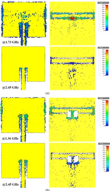
To demonstrate the effects of the DGS on the antenna radiation mechanism, the surface current plots of Antenna B at 1.73 GHz and 2.45 GHz and of Antenna C at 1.36 GHz and 2.45 GHz are presented in Fig. 6(a) and 6(b), all in 0° phase angles. The rainbow scale bar provides surface current intensities in A/m whose maximum value is clamped at 600 A/m for better demonstration of the difference in the surface currents. The selected frequencies are important, since 1.73 GHz is the 𝑓( of Antenna B, 1.36 GHz is the 𝑓( of Antenna C and 2.45 GHz is the 𝑓( of Antenna A. The figure shows that at 1.73 GHz, the surface current densities on CSRR structure is much stronger than that of 2.45 GHz revealing that CSRR has an active role in the radiation mechanism at 1.73 GHz. Similarly, at 1.36 GHz, the surface current densities on CSRR-D structure are much stronger than that of 2.45 GHz revealing that CSRR-D has an active role in the radiation mechanism at 1.36 GHz.
FIGURE 6. Surface current plots on (a) Antenna B at 1.73 GHz and 2.45
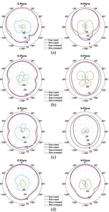
GHz and (b) Antenna C at 1.36 GHz and 2.45 GHz in 0° phase angle. Fig. 7 shows the simulated and the measured E- and H-plane radiation patterns in terms of antenna gains in dBi with respect to the elevation angle θ. In general, the results are compatible with each other. Although at first sight there seem to exist some discrepancies especially in the cross-polarization (i.e., crosspol) results, in fact they are close to each other in linear scale. On the other hand, the discrepancies observed in the co-polarization (i.e., copol) results may be due to imperfect fabrications, imperfect soldering process of the connectors, and measurement errors. The radiation patterns of Antenna B and C present increased backward radiations due to the CSRR and CSRR-D slots patterned in the ground planes in comparison to the reference antenna. This may explain the reduced directivity of the designs with the defected ground structures.
(a)
(b)
(c)
(d)
FIGURE 7. Radiation patterns in terms of gain (dBi) with respect to elevation angle θ obtained by simulations and experiments. (a) Antenna A @ 2.45 GHz by simulation and @ 2.46 GHz by experiment. (b) Antenna B @ 1.73 GHz by simulation @ 1.75 GHz by experiment. (c) Antenna C @ 1.36 GHz by simulations and experiments. (d) Antenna D @ 1.36 GHz by simulations and experiments.
The remaining characterization results obtained by the simulations and experiments are % BW and VSWR where %
BW is calculated at -10 dB. As an observation, the % BW of Antenna C increases slightly as compared to Antenna B and decreases slightly as compared to Antenna A, however the changes are not found to be significant. On the other hand,
VSWR values do not exceed 1.27 in general which is the
proof of good impedance matchings. All the results are tabulated in Table II for better visualization. The simulation and experimental gain values in Table II represent the
maximum gains obtained by considering both E and H-planes for each antenna.
TABLEII.Simulation and experimental results for the designed antennas Parameters Antenna Structures
Ant. A Ant. B Ant. C Ant. D
f0 (GHz) Sim. 2.45 1.73 1.36 1.36 Exp. 2.47 1.75 1.36 1.37 % BW Sim. 1.45 1.02 1.30 0.96 Exp. 1.58 0.88 1.13 0.94 VSWR Sim. 1.03 1.07 1.08 1.13 Exp. 1.02 1.23 1.27 1.05 ecd (dB) Sim. −0.61 −1.25 −0.92 −1.08 D (dBi) Sim. 7.08 5.33 4.12 7.25 G (dBi) Sim. 6.48 4.08 3.20 6.19 Exp. 6.65 2.22 1.77 7.97 ka Sim. 1.43 1.01 0.79 1.39 Exp. 1.44 1.02 0.79 1.39 % ESR Sim. 0 29.39 44.49 0 Exp. 0 29.15 44.94 0
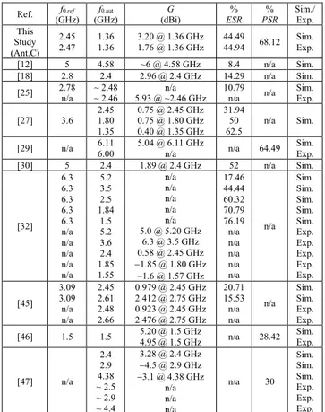
For the antenna performance comparisons, the specific antenna parameters (i.e., 𝑓(, and G) together with the % ESR and % PSR values are listed in Table III, if exists, regarding the proposed Antenna C together with the other single microstrip antennas reported in literature whose DGS are composed of CSRRs. Herein multiple input multiple output (MIMO) antenna designs [22,44,53] are not included in the comparison table since the usage of multiple antennas in the design may affect the individual antenna performances and this may cause an unfair comparison. In addition, the CSRR based DGS structures reported in reference [48] are also not included in the comparison table since the study mainly focuses on the sensor application rather than designing a small antenna thus the fundamental antenna parameters such as gain, efficiency and radiation pattern are not provided.
It is important to note that the % ESR values presented in Table III are calculated by using Equation (1), which is based on the resonance frequency, and % PSR values are calculated considering the reduction in the patch areas reported in each study. Since all the studies do not include both simulation and experimental analyses, Table III includes only simulation or experimental results for some references.
The studies that are used in the comparison can be classified in four groups: The first group consists of the studies which promise higher gain values, however lower %
ESR than our study [12,25,32]. In contrary, the second group
consists of the studies which promise lower gain values, however higher % ESR [27,30,32]. The third group consists of the studies which promise both lower gain and lower %
ESR [18,45]. It is important to note that references [32] and
[45] applied some major geometrical modifications on the metallic patch in addition to DGS structure. Especially, the modifications made by reference [32] in their final design increased the area of the radiating element which may be a
E. M. Kucukoner et al.
handicap in the concern of ESR and PSR. Finally, for the fourth group, references [29], [46], and [47] propose lower %
PSR values, however higher gain values than that of this
study. Among the references discussed in Table III, especially references [12], [25], [32], [45], [46], and [47] offers more complex DGS patterns as compared to this study. As the result, the proposed Antenna C promises an advantage at least on one parameter under interest as compared with the closely related literature.
TABLEIII.Performance comparisons of Antenna C with the other microstrip antennas whose DGS are composed of CSRRs
Ref. f0,ref
(GHz) (GHz) f0,aut (dBi) G ESR % PSR % Sim./ Exp. This Study (Ant.C) 2.45 2.47 1.36 1.36 3.20 @ 1.36 GHz 1.76 @ 1.36 GHz 44.49 44.94 68.12 Sim. Exp. [12] 5 4.58 ~6 @ 4.58 GHz 8.4 n/a Sim. [18] 2.8 2.4 2.96 @ 2.4 GHz 14.29 n/a Sim. [25] 2.78 n/a ~ 2.48 ~ 2.46 5.93 @ ~2.46 GHz n/a 10.79 n/a n/a Sim. Exp. [27] 3.6 2.45 1.80 1.35 0.75 @ 2.45 GHz 0.75 @ 1.80 GHz 0.40 @ 1.35 GHz 31.94 50 62.5 n/a Sim. [29] n/a 6.11 6.00 5.04 @ 6.11 GHz n/a n/a 64.49 Sim. Exp. [30] 5 2.4 1.89 @ 2.4 GHz 52 n/a Sim. [32] 6.3 6.3 6.3 6.3 6.3 n/a n/a n/a n/a n/a 5.2 3.5 2.5 1.84 1.5 5.2 3.6 2.4 1.85 1.55 n/a n/a n/a n/a n/a 5.0 @ 5.20 GHz 6.3 @ 3.5 GHz 0.58 @ 2.45 GHz -1.85 @ 1.80 GHz -1.6 @ 1.57 GHz 17.46 44.44 60.32 70.79 76.19 n/a n/a n/a n/a n/a n/a Sim. Sim. Sim. Sim. Sim. Exp. Exp. Exp. Exp. Exp. [45] 3.09 3.09 n/a n/a 2.45 2.61 2.48 2.66 0.979 @ 2.45 GHz 2.412 @ 2.75 GHz 0.923 @ 2.45 GHz 2.476 @ 2.75 GHz 20.71 15.53 n/a n/a n/a Sim. Sim. Exp. Exp. [46] 1.5 1.5 5.20 @ 1.5 GHz 4.95 @ 1.5 GHz n/a 28.42 Sim. Exp.
[47] n/a 2.4 2.9 4.38 ~ 2.5 ~ 2.9 ~ 4.4 3.28 @ 2.4 GHz -4.5 @ 2.9 GHz -3.1 @ 4.38 GHz n/a n/a n/a n/a 30 Sim. Sim. Sim. Exp. Exp. Exp. V. CONCLUSION
In this study, the effects of using DGS, composed of CSRR and CSRR-D structures, on electrical size, percentage bandwidth, efficiency, directivity, and gain for the rectangular microstrip patch antenna are investigated in comparison to the ordinary rectangular microstrip antenna. The results show that both DGS based antennas which are studied in the study; reduce the electrical size, however, decrease the gain due to the reduced directivity as compared to the reference antenna because of the back radiation caused by the defected ground design. As compared to the antenna having DGS with CSRR, the antenna having DGS with CSRR-D provided better ESR, however lower gain values. Specially, a 29.39 % ESR in simulation and a 29.15 % ESR in experiment are obtained for Antenna B (i.e., antenna with CSRR) with a 4.08 dBi gain in simulation and a 2.22 dBi
gain in experiment. On the other hand, a 44.49 % ESR in simulation and a 44.94 % ESR in experiment, moreover a 68.12 % PSR both in simulation and experiment are obtained for Antenna C (i.e., antenna with CSRR-D) with a 3.20 dBi gain in simulation and a 1.77 dBi gain in experiment. Considering the antenna designs having CSRR based DGS structures in literature, Antenna C may be a good alternative in terms of its % ESR value, % PSR value, gain value and simple geometry for possible mobile communication applications. The design comes together with the flexibility of carrying the operating frequency to the other frequencies under interest (e.g., 5G frequencies) by simply modifying the structure sizes.
ACKNOWLEDGMENT
This work was supported in part by the Suleyman Demirel University Coordinatorship of Scientific Research Projects (Süleyman Demirel Universitesi Bilimsel Araştırma Projeleri Koordinasyon Birimi) under Grant 4085-YL1-14. We acknowledge Department of Electrical and Electronics Engineering, Middle East Technical University, Ankara for providing us the opportunity to access the anechoic chamber for the antenna gain and radiation pattern measurements. We also acknowledge Ms. Damla Alptekin and Mr. Savas Karadag for their effort and help during the gain and radiation pattern measurements.
REFERENCES
[1] J. S. Colburn, and Y. Rahmat-Samii, “Patch antennas on externally perforated high dielectric constant substrates,” IEEE Trans. Antennas
Propag., vol. 47, no. 12, pp. 1785-1794, Dec. 1999.
[2] L. Desclos, Y. Mahe, S. Reed, G. Pollasne, and S. Toutain, “Patch antenna size reduction by combining inductive loading and short-points technique,” Microwave Opt. Technol. Lett., vol. 30, no. 6, pp. 385-386, Sep. 2001.
[3] H. Oraizi, and B. Rezaei, “Dual-banding and miniaturization of planar triangular monopole antenna by inductive and dielectric loadings,” IEEE Antennas Wirel. Propag. Lett., vol. 12, pp.1594-1597, Dec. 2013
[4] P. M. T. Ikonen, K. N. Rozanov, A. V. Osipov, P. Alitalo, and S. A. Tretyakov, “Magnetodielectric substrates in antenna miniaturization: potential and limitations,” IEEE Trans. Antennas Propag., vol. 54, no. 11, pp. 3391-3399, Nov. 2006.
[5] R. O. Ouedeaogo, E. J. Rothwell, A. R. Diaz, K. Fuchi, and A. Temme, “Miniaturization of patch antennas using a metamaterial-inspired technique,” IEEE Trans. Antennas Propag., vol. 60, no. 5,pp. 2175-2182, May 2012.
[6] S. Painam, and C. Bhuma, “Miniaturizing a microstrip antenna using metamaterials and metasurfaces,” IEEE Antennas Propag. Mag., vol. 61, no. 1, pp.91-135, Feb. 2019.
[7] A. Erentok, and R. W. Ziolkowski, “Metamaterial-inspired efficient electrically small antennas,” IEEE Trans. Antennas Propag., vol. 56, no. 3, pp. 691-707, Apr. 2008.
[8] O. Turkmen, G. Turhan-Sayan, and R. W. Ziolkowski, “Single-, dual-, and triple-band metamaterial-inspired electrically small planar magnetic dipole antennas,” Microwave Opt. Technol. Lett., vol. 56, no. 1, pp. 83-87, Jan. 2014.
[9] M. Ramzan, and K. Topalli, “A miniaturized patch antenna by using a CSRR loading plane,” Int. J. Antennas Propag., vol. 2015, pp. 1-9, Jul. 2015.
[10] R. B.Waterhouse, S. D. Targonski, and D. M. Kokotoff, “Design and performance of small printed antennas,” IEEE Trans. Antennas
[11] H. A. Atallah, A. B. Abdel-Rahman, K. Yoshitomi, and R. K. Pokharel, “Mutual coupling reduction in MIMO patch antenna array using complementary split ring resonators defected ground structure,” Appl. Comput. Electromagn. Soc. J., vol. 31, no. 7, pp. 737-743, Jul. 2016.
[12] M. M. Bait-Suwailam, and H. M. Al-Rizzo, “Size reduction of microstrip patch antennas using slotted complementary split ring resonators,” in Proc. Technological Advances in Electrical,
Electronics and Computer Engineering (TAEECE), Turkey, 2013,
pp. 528-531.
[13] U. Chakraborty, S. K. Chowdhury, and A. K. Bhattacharjee, “Frequency tuning and miniaturization of square microstrip antenna embedded with T-shaped defected ground structure,” Microwave
Opt. Technol. Lett., vol. 55, no. 4, pp. 869-872, Apr. 2013.
[14] F. Chetouah, S. Aidel, N. Bouzit, and I. Messaoudene, “A miniaturized printed monopole antenna for 5.2-5.8 GHz WLAN applications,” Int. J. RF Microw. Comput. Aided Eng., vol. 28, no. 5, pp. 1-8, Jan. 2018.
[15] H. Elftouh, N. A. Touhami, M. Aghoutane, S. E. Amrani, A. Tazon, and M. Boussouis, “Miniaturized microstrip patch antenna with defected ground structure,” Prog. Electromagn. Res. C, vol. 55, pp. 25-33, Nov. 2014.
[16] E. Fritz-Andrade, J. A. Tirado-Mendez, H. Jardon-Aguilar, and R. Flores-Leal, “Application of complementary split ring resonators for size reduction in patch antenna arrays,” J. Electromagn. Waves
Appl., vol. 31, no.16, pp. 1755-1768, Aug. 2017.
[17] C. Garg, and M. Kaur, “A review of defected ground structure (DGS) in microwave design,” Int. J. Innovative Res. Electr. Electron.
Instrum. Control Eng., vol. 2, no. 3, pp. 1285-1290, Mar. 2014.
[18] S. Goswami, K. Sarmah, A. Sarma, K. K. Sarma, and S. Baruah, “Design of a CSRR based compact microstrip antenna for image rejection in RF down-converter based WLAN receivers,” Int. J.
Electron. Commun., vol. 74, pp.128-134, Feb. 2017.
[19] E. M. Kucukoner, U. Kose, and E. Ekmekci, “Numerical investigation of the effect of resonator position etched on defected ground structure composed of a complementary split ring resonator with dumbbell designed for microstrip patch antenna on electrical size,” in Proc. Int. Conf. on Electrical and Electronics Engineering
(ELECO), Bursa, Turkey, 2016, pp. 543-546.
[20] F. Li, Y. C. Jiao, L. S. Ren, J. G. Gong, and B. Chen. “Compact double T-shaped slots antenna with a rectangular patch for bandwidth enhancement,” in Proc. Int. Symp. on Antennas,
Propagation & EM Theory (ISAPE), Guangzhou, China, 2010, pp.
286-288.
[21] M. Li, M. Lu, and T. J. Cui. “Novel miniaturized dual band antenna design using complementary metamaterial,” Int. Workshop on
Metamaterials, 2008, pp.374-376.
[22] A. C. J. Malathi, and D. Thiripurasundari, “CSRR loaded 2×1 triangular MIMO antenna for LTE band operation,” Advanced
Electromagnetics, vol. 6, no. 3, pp. 78-83, Oct. 2017.
[23] G. P. Mishra, and B. B. Mangaraj, “Miniaturised microstrip patch design based on highly capacitive defected ground structure with fractal boundary for X-band microwave communications,” IET
Microw. Antennas Propag., vol. 13, no. 10, pp. 1593-1601, Aug.
2019.
[24] O. Oulhaj, N. A. Touhami, M. Aghoutane, and A. Tazon, “A miniature microstrip patch antenna array with defected ground structure,” Int. J. Microw. Opt. Technol., vol. 11, no. 1, pp.32-39, Jan. 2016.
[25] R. Pandeeswari, and S. Raghavan, “Microstrip antenna with complementary split ring resonator loaded ground plane for gain enhancement,” Microwave Opt. Technol. Lett., vol. 57, no. 2, pp. 292-296, Feb. 2015.
[26] M. S. Rabbani, and H. Ghafouri-Shiraz, “Microstrip antennas for X-band and MM-wave frequencies based on diamond shape defected ground structure and size extension method,” Microwave Opt.
Technol. Lett., vol. 58, no. 12, pp. 2836-2841, Dec. 2016.
[27] V. Rajeshkumar, and S. Raghavan. “A compact CSRR loaded dual band microstrip patch antenna for wireless applications,” in Proc. IEEE Int. Conf. on Computational Intelligence and Computing Research (ICCIC), India, 2013.
[28] M. Rashid, M. E. Munir, J. Khan, and K. Mahmood, “Design of miniaturized multiband microstrip patch antenna using defected ground structure,” Int. J. Adv. Comput. Sci. Appl., vol. 9, no. 6, pp. 168-173, Jul. 2018.
[29] F. Raval, Y. P. Kosta, and H. Joshi, “Reduced size patch antenna using complementary split ring resonator as defected ground plane,”
Int. J. Electron. Commun., vol. 69, no. 8, pp. 1126-1133, Apr. 2015.
[30] A. Reddaf, F. Djerfaf, K. Ferroudji, M. Boudjerda, K. Hamdi-Cherif, and I. Bouchachi, “Design of dual-band antenna using an optimized complementary split ring resonator,” Appl. Phys. A, vol. 125, no. 3, pp. 1-9, Feb. 2019.
[31] B. R. S. Reddy, and D. Vakula, “Compact zigzag-shaped-slit microstrip antenna with circular defected ground structure for wireless applications,” IEEE Antennas Wirel. Propag. Lett., vol. 14, pp. 678-681, Mar. 2015.
[32] S. I. Rosaline, and S. Raghavan, “CSRR-based compact penta band printed antenna for GPS/GSM/WLAN/WiMAX applications,”
Microwave Opt. Technol. Lett., vol. 57, no. 7, pp. 1538-1542, Jul.
2015.
[33] A. Z. Shari, A. A. A. Aziz, N. Sarbani, and M. T. Ali, “A design of rectangular aeroplane shape defected ground structure (RADGS) antenna for 2.4 GHz applications,” in. Proc. Int. Conf. on Media Education and Training (ICMET), Selangor, Malaysia, 2015. pp. 13-16.
[34] A. Sharma, and R. K. Gangwar, “Compact quad-band cylindrical dielectric resonator antenna with complementary C-Shaped defected ground structure,” Microwave Opt. Technol. Lett., vol. 58, no. 3, pp. 611-615, Mar. 2016.
[35] M. K. Verma, B. K. Kanaujia, J. P. Saini, and P. Saini, “A novel circularly polarized gap-coupled wideband antenna with DGS for X/Ku-band applications,” Electromagnetics, vol. 39, no. 3, pp. 186-197, Dec. 2019.
[36] X. Zhao, and S. Riaz, “A dual-band frequency reconfigurable MIMO patch-slot antenna based on reconfigurable microstrip feedline,”
IEEE Access, vol. 6, pp.41450-41457, Jul. 2018.
[37] H. R. Stuart, and A. Pidwerbetsky, “Electrically small antenna elements using negative permittivity resonators,” IEEE Trans.
Antennas Propag., vol. 54, no. 6, pp. 1644-1653, Jun. 2006.
[38] G. J. N. Lenin, R. Vimala, R. Sornakeerthi, and K. R. A. Britto, “Design of low profile wide band solplant with DGS,” ARPN J. Eng.
Appl. Sci., vol. 11, no. 3, pp. 1729-1734, Jan. 2016.
[39] S. C. Basaran, “A compact dual-wideband antenna based on complementary split-ring resonator,” Microwave Opt. Technol. Lett., vol. 54, no. 8, pp. 1917-1920, Aug. 2012.
[40] S. C. Basaran, U. Olgun, and K. Sertel, “Multiband monopole antenna with complementary split-ring resonators for WLAN and WiMAX applications,” Electron. Lett., vol. 49, no. 10, pp. 636-637, May 2013.
[41] H. Maema, and T. Fukusako, “Radiation efficiency improvement for electrically small and low-profile antenna by stacked elements,”
IEEE Antennas Wirel. Propag. Lett., vol. 13, pp. 305-308, 2014.
[42] R. Pandeeswari, and S. Raghavan, “Broadband monopole antenna with split ring resonator loaded substrate for good impedance matching,” Microwave Opt. Technol. Lett., vol. 56, no. 10, pp. 2388-2392, Oct. 2014.
[43] R. H. Patel, T. Upadhyaya, and A. Desai, “Electrically small inverted L planar patch antenna for wireless application,” Microwave Opt.
Technol. Lett., vol. 60, no. 10, pp. 2351-2357, Feb. 2018.
[44] M. U. Khan, and M. S. Sharawi, “A 2×1 multiband MIMO antenna system consisting of miniaturized patch elements,” Microwave Opt.
Technol. Lett., vol. 56, no. 6, pp. 1371-1375, Jun. 2014.
[45] M. S. Rao, and P. I. Basarkod, “A novel complementary slotted split ring resonator loaded truncated arc patch antenna with enhanced performance,” Prog. Electromagn. Res. C, vol. 101, pp. 203-218, May. 2020.
[46] Y. G. Adhiyoga, C. Apriono, and E. T. Rahardjo, “Radiation characteristics of artificial magneto-dielectric antenna loaded with split-ring resonator array,” Advanced Electromagnetics, vol. 9, no. 3, pp. 32-38, Dec. 2020.
[47] M. A. Abdalla, W. W. Wahba, and A. A. Allam, “Analysis and design of a compact CRLH inspired – defected ground resonators for
E. M. Kucukoner et al.
Triple Band Antenna Applications,” Int. J. Eng. Sci. Technol., vol. 23, no. 1, pp. 114-122, Feb. 2020.
[48] J. Yeo, and J. Lee, “Design of a high-sensitivity microstrip patch sensor antenna loaded with a defected ground structure based on a complementary split ring resonator,” Sensors, vol. 20, no. 7064, pp. 1-18, Dec. 2020.
[49] A. Jaiswal, R. K. Sarin, B. Raj, and S. Sukhija, “A novel circular slotted microstrip-fed patch antenna with three triangle shaped defected ground structure for multiband applications,” Advanced
Electromagnetics, vol. 7, no. 3, pp. 56-63, Aug. 2018.
[50] S. Sah, M. R. Tripathy, and A. Mittal, “Multiband and miniaturized dual layer antenna incorporated with FSS and DGS,” Advanced
Electromagnetics, vol. 7, no. 1, pp. 1-6, Jan. 2018.
[51] S. Riaz, X. Zhao, and S. Geng, “A frequency reconfigurable MIMO antenna with agile feedline for cognitive radio applications,” Int J RF
Microw. Comput. Aided Eng., vol. 30, no. 3, pp. 1-9, Dec. 2019.
[52] V. Kumar, and Y. Wu, “Metamaterial based circular disc patch antenna miniaturization,” Advanced Electromagnetics, vol. 7, no. 5, pp. 137-144, Dec. 2018.
[53] M. S. Sharawi, M. U. Khan, A. B. Numan, and D. N. Aloi, “A CSRR loaded MIMO antenna system for ISM band operation,” IEEE Trans.
Antennas Propag., vol. 61, no. 8, pp. 4265-4274, Aug. 2013.
[54] M. Yang, Z. N. Chen, P. Y. Lau, X. Qing, and X. Yin, “Miniaturized patch antenna with grounded strips,” IEEE Trans. Antennas Propag., vol. 63, no. 2, pp. 843-848, Feb. 2015.
[55] K. Buell, H. Mosallaei, and K. Sarabandi, “A substrate for small patch antennas providing tunable miniaturization factors,” IEEE