PECVD grown SiN photonic crystal micro-domes for the light
extraction enhancement of GaN LEDs
M. Genç*
a,b,c, V. Sheremet
d, İ. Altuntaş
f, İ. Demir
f, E. Gür
e, S. Elagöz
f, O. Gülseren
d, Ü. Özgür
h, V.
Avrutin
h, H. Morkoç
hand A. Aydınlı
ga
Tyndall National Institute, Cork, Ireland;
bSabancı University, Department of Electronics
Engineering, İstanbul, Turkey;
cErmaksan Optoelectronic R&D Center, Bursa, Turkey;
dBilkent
University, National Nanotechnology Research Center (UNAM), Ankara, Turkey;
eAtatürk
University, Department of Physics, Erzurum, Turkey;
fCumhuriyet University, Nanophotonics
Research and Application Center, Sivas, Turkey;
gUludağ University, Department of Electrical and
Electronics Engineering, Bursa, Turkey;
hVirginia Commonwealth University, Department of
Electrical and Computer Engineering, Richmond, VA, USA
[email protected]
[email protected]
ABSTRACT
In this work, the effect of introducing a photonic crystal network of silicon nitride (SiN) micro-domes on the backside of silver coated gallium nitride (GaN) based light emitting diodes (LEDs) was studied. First, sapphire side of the top emitting LEDs, which is the bottom surface of the LEDs, is coated with silver (Ag). Light emitted towards the sapphire substrate is reflected upwards to the top surface and the amount of light extracted from the LED is expected to increase. In an alternative approach, SiN micro-domes forming a two dimensional photonic crystal, 2 µm in diameter and 80 nm in height in average, are deposited on the light emitting surface of the device with a period of 2 µm. Coating the backside with Ag has increased the efficiency of a top emitting LED by 11%. By introducing the SiN photonic crystal onto the Ag backside coated sample, total internal reflection is reduced via scattering and the amount of light emitted has been increased by 30% at 5·104 mA/cm2. Integration of SiN micro-domes with Ag coating has significantly impacted light extraction which has been shown to increase the efficiency of GaN based LEDs. Fabrication process and the results are discussed in detail. Keywords: Light extraction, Si3N4 micro-domes, LED performance, light emitting diodes
1. INTRODUCTION
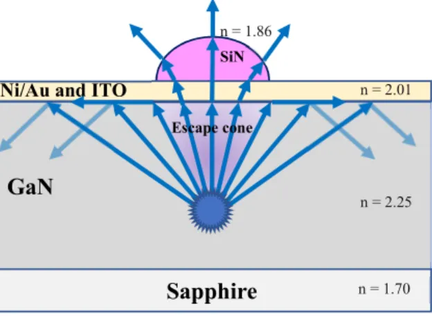
High brightness LEDs have been used in various applications including next generation displays such as augmented and virtual reality (AR\VR) headsets, micro-LED displays, communication, automotive lighting and general lighting for optoelectronics. Many research activities have been focused to achieve higher brightness LEDs with larger quantum efficiencies. One of the biggest problems limiting the brightness of LEDs is the total internal reflection, which reduces the photon removal efficiency of the LEDs [1]. Variety of design techniques have been studied to enhance light extraction efficiency, such as surface roughening of sapphire or ITO, chip forming (shaping), and the use of photonic crystals. In this context, the refractive indices of the sapphire substrate and the epitaxial layers grown on it, are very large relative to air. Refractive index of sapphire is n = 1.7 at 450 nm wavelength and the refractive index of GaN layers is 2.25. If we neglect the refractive indices of the possible thin InGaN and AlGaN layers in between, the Fresnel equations show that the exact total internal reflection angle is quite small, such that the light produced in the InGaN quantum wells can hardly escape the LED. Interfaces of GaN with air, sapphire with air, sapphire with GaN, emitting light from Fresnel cones is limited by total internal reflection. The light cone between GaN and air is shown schematically in figure 1. Various strategies have been developed to overcome the limitations of the light cone. One of the most commonly used methods is to overcome the cone limitation of light is by increasing the scattering between air and sapphire or air and GaN [2]. In this work, scattering was used by coating a thin film by adjusting of refractive index on GaN or sapphire and patterning the corresponding film.
Figure 1. Escape cone and total internal reflection of light.
The refractive index of SiN thin films can be adjusted by changing the PECVD growth parameters such as gas flow rates and growth temperatures. The SiN thin film coated at the interface where scattering is achieved, is then patterned by photolithography to increase the light extraction efficiency [3].
2. EXPERIMENTAL
InGaN MQW based LED structures were grown by metal organic chemical vapor deposition (MOCVD) system on sapphire substrate. Epitaxial layers consist of 10 µm undoped GaN grown by in situ nano-ELO technique, followed by a 4 µm thick n-GaN (3x1018 cm-3), a 60 nm In
0.01GaN0.99 stress compensation layers, a 7 step graded InxGa1-xN (x = 0.04 to 0.1 with 3 nm thickness for each step) electron injector layer, 6 x 2 nm In0.15Ga0.85N quantum wells separated by 3 nm-thick In0.06Ga0.94N barriers, and finally a 100 nm p-GaN (4x1017 cm-3). Figure 2 shows the grown epitaxial structure. The step graded electron injector (SEI) is included in the structure to help to cool down the electrons prior to injection into the MQW region and thus mitigate the electron overflow [4].
Figure 2. Cross-sectional view of LED structure
Fabrication of the LED device is as follows; square mesas of 1 mm2 were formed by ICP etching with BCl
3:Cl2 gases. LEDs had interdigitated electrode patterns with distance from contact pads to the edge of etched mesa equals to 150 µm. Ohmic contacts to n-GaN were formed using a Ti(30 nm)/Al(50 nm)/TiB2(50 nm)/Au(70 nm) metal stack which was subjected to rapid thermal annealing (RTA) in N2 ambient at T= 800 oC for 30 second after electron beam evaporation. For current spreading layer and ohmic contact to p-GaN, a Ni(5 nm)/Au(5 nm)/ITO(120 nm) stack was used with Ti(30 nm)/Au(50 nm) contact pads on the ITO. ITO thin film was grown 120 nm on top of the p-GaN layer by RF sputtering.
GaN
Sapph re
SiN
Ni/Au and ITO
n = 1.86
Escape cone
n = 2.01
n = 1.70 n = 2.25
a) b) c)
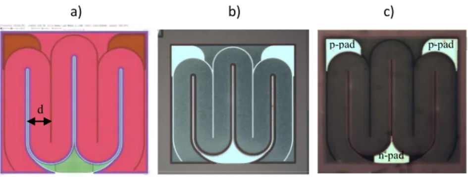
Figure 3. a) 1 mm2 single chip design (photomask) with d=150 µm, b) fabricated LED chip with pre-pass and silver, c)
additional SiNmicro-domes located everywhere except at the p- and n- contact pads.
In this study, the sample was fabricated and denoted as pre-passivated, pre-passivated and silver and lastly pre-passivated, silver and SiN micro-domes. The pre-passivation was employed with PECVD-deposited SiO2 of 250 nm thickness immediately after ICP mesa etching. After the metal deposition on the p-GaN side, Finally, 230 nm SiN was grown by the PECVD technique on top of the SiO2 passivation layer. For pre-passivation and silver sample, then, 160 nm silver was deposited to collect escaping light from sapphire side. For light extraction improvement, micro-domes were formed with the assist of UV lithography followed by etching in buffered oxide etchant (BOE). Windows in SiN passivation layer were gained to access just the contact pads on the n-GaN and contact pads on the current spreading ITO layers. Photomask design and optical microscope images of fabricated LED chips were shown in figure 3. Shematic of the fabricated photonic crystals and the optical microscope images taken after fabrication were given in figure 4. Electrical properties of fabricated LED dies were measured using a Keithley 2430 source and an HP 4142B monitor unit. Optical properties were measured by Instrument Systems spectrometer CAS 140CT. Ohmic contact resistivities were measured by using transmission line method (TLM) with linear and circular contact pad geometries. For linear TLM measurements, 75x450 µm2 contact pads were used with separations of 20, 40, 60, 80, 100 and 150 µm. For circular TLM measurements inner contact pads had diameters of 50, 80, 100 and 150 µm with a constant ratio between outer andinner contact diameters of 2 [5, 6].
a)
b)
Figure 4. a) 3D drawings of SiN photonic crystals b) optical microscope pictures of 2D photonic crystals that was fabricated by using reflow method.Blue arrows point to SiN micro-domes.
n-pad p-pad p-pad
3. RESULTS
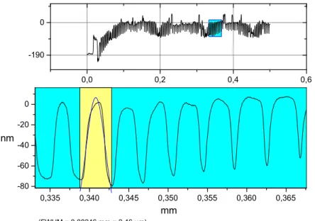
The shape and the heights of the micro domes of the photonic crystals were analyzed using a dektak surface profilometer. 2 µm scanning stylus was chosen to measure hills and valleys.
0,0 0,2 0,4 0,6 -190 0 0,335 0,340 0,345 0,350 0,355 0,360 0,365 -80 -60 -40 -20 0 (FWHM = 0,00246 mm = 2,46 µm) nm mm
Figure 5. Surface profiles of photonic crystal micro-domes.
The heights of micro-domes were measured as 80 nm (average), while the width of micro-domes are 2.46 µm with 2 µm spacing between them. We note that micro-domes are uniform in size and uniformly distributed over the chip. As shown in figure 5.
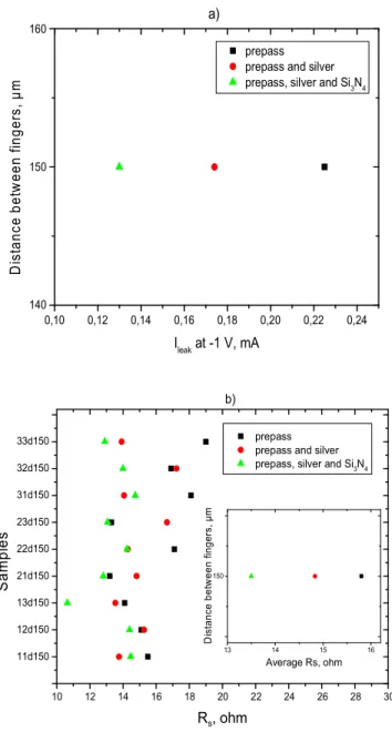
11d150 12d150 13d150 21d150 22d150 23d150 31d150 32d150 33d150 10 12 14 16 18 20 22 24 26 28 30 prepass prepass and silver prepass, silver and Si3N4
Rs, ohm S a m p le s 150 13 14 15 16 D is ta n ce b e tw e e n fi n g er s, µ m Average Rs, ohm b)
Figure 6. a) Leakage current values at -1 Volt and b) average series resistance values of different LED dies
Series resistance was obtained for the LED with pre-passivation, silver and SiN has been lowered by 14.6 % compared to that of the pre-passivated sample. On the other hand, the leakage current for the same sample has decreased to 25.3% compared to that of the pre-passivation and silver sample (figure 6). It seems that the SiN passivation has improved the device performances. 140 150 160 0,10 0,12 0,14 0,16 0,18 0,20 0,22 0,24 prepass prepass and silver prepass, silver and Si3N4
Ileak at -1 V, mA D is ta nc e b et w ee n fi ng er s, µ m a)
4. ACKNOWLEDGEMENT
This work is supported by Scientific and Technical Research Council of Turkey, (TUBITAK Grants no: 113G042 and 115E109). We thank to Advanced Research Laboratory of Bilkent University and Ermaksan Optoelectronic R&D Center for the use of fabrication and characterization equipments.
5. REFERENCES
[1] Kyeong-Jae Byeon et al., “Fabrication of two-dimensional photonic crystal patterns on GaN-based light-emitting diodes using thermally curable monomer-based nanoimprint lithography”, Appl. Phys. Lett. 91, 091106 (2007). [2] J. J. Wierer et al., (2005), III-Nitride LEDs with photonic crystal structures, Proc. of SPIE Vol. 5739.
[3] Kim et al., “Elimination of total internal reflection in GaInN light-emitting diodes by graded-refractive-index micropillars”, Appl. Phys. Lett. 93, 221111 2008.
[4] H. Morkoç, Handbook of Nitride Semiconductors and Devices, Vol. 1: Materials Properties, Physics and Growth, WILEY-VCH Verlag GmbH &Co. KGaA, Weinheim, 2008.
[5] V. Sheremet et al. / “Two-step passivation for enhanced InGaN/GaN light emitting diodes with step graded electron injectors, Superlattices and Microstructures”, 113 (2018) 623-634.
[6] M. Genç et al., “Distributed contact flip chip InGaN/GaN blue LED; comparison with conventional LEDs”, Superlattices and Microstructures 128 (2019) 9–13.
As a summary, photonic crystal design was used for situations where light emerges from the top [2]. In order to increase the emission of light, SiN photonic crystals were grown in PECVD system in 2.46 µm diameter, 80 nm height and 2 µm periods, and eventually pattern structures were formed by reflow method. It is clearly shows that additional silver and SiN, has significantly impacted of light extraction enhancement.
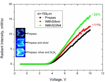
The total power values of the LED sample were increased by 29% for samples with 150 µm finger spacing due to SiN micro-dome photonic crystals inclusion as shown in figure 7. Inset shows the microscope images of the LEDs when they are emitting. The brightness of the light increases gradually by using additional Ag back contact and Si3N4 micro domes. It is clear from the figures that SiN micro-domes significantly improves the light extraction.
Figure 7. Radiant intensity values of device with pre-passivation, with silver and with Si3N4 in terms of voltage
1,0 1,2 1,4 1,6 1,8 2,0 6 7 8 1.0 1.2 1.4 1.6 1.8 2.0 6 7 8 R ad ia nt In te ns ity , m W /s r Voltage, V Prepass WithSilver WithSi3N4 R ad ia nt In te ns ity , m W /s r Voltage, V Prepass
Prepass and silver