Area-Selective Atomic Layer Deposition Using an Inductively
Coupled Plasma Polymerized Fluorocarbon Layer: A Case Study for
Metal Oxides
Ali Haider,
*
,†,‡Petro Deminskyi,
‡Talha M. Khan,
†,‡Hamit Eren,
†,‡and Necmi Biyikli
*
,§†Institute of Materials Science and Nanotechnology, Bilkent University, Ankara 06800, Turkey ‡UNAM - National Nanotechnology Research Center, Bilkent University, Ankara 06800, Turkey
§Electrical and Computer Engineering Department, Utah State University, Logan, Utah 84322, United States
*
S Supporting InformationABSTRACT: Area-selective atomic layer deposition (AS-ALD) has attracted immense attention in recent years for self-aligned accurate pattern placement with subnanometer thickness control. Here, we demonstrate a methodology to achieve AS-ALD by using inductively couple plasma (ICP) grown fluorocarbon polymer film as hydrophobic blocking layer for selective deposition. Our approach has been tested for metal-oxide materials including ZnO, Al2O3, and HfO2. Contact angle, X-ray photoelectron spectroscopy (XPS),
spectroscopic ellipsometer, and scanning electron microscopy (SEM) measurements were performed to investigate the blocking ability of plasma polymerizedfluorocarbon layers against ALD-grown metal-oxide films. A considerable growth inhibition for ZnO has been observed onfluorocarbon coated Si(100) surfaces, while the same polymerized surface caused a relatively slow nucleation for HfO2films. No growth selectivity was obtained for Al2O3films, displaying almost the same nucleation behavior on Si andfluorocarbon surfaces. Thin film patterning has been demonstrated using this strategy by growing ZnO on lithographically patternedfluorocarbon/Si samples. High resolution SEM images and XPS line scan confirmed the successful patterning of ZnO up to afilm thickness of ∼15 nm.
■
INTRODUCTIONMicro and nanoscale film patterning is an essential part of modern microelectronics industry, being the essential ingre-dients of Si-based CMOS transistor technology. As device scaling proceeds toward sub-10 nm era where process tolerances become atomic-scale, the adoption of alternative nanoscale process integration schemes become critical for both Moore’s law (extension of device down-scaling) and beyond Moore (novel device concepts). Nanoscale process integration demands novel nanopatterning techniques in compliance with the requirements of feature generation devices. Conventionally, top-down subtractive (etch) or additive (deposition/lift-off) processes in conjunction with various lithography techniques is employed to achieve film patterning, which becomes increasingly challenging due to the ever-shrinking alignment requirements.1−3 To reduce the complexity burden of litho-graphic alignment in future technology nodes, self-aligned processes such as selective deposition and selective etching might provide vital solutions.
In recent years, area-selective atomic layer deposition (AS-ALD) has attracted significant attention as a powerful alternative path for the realization of nanoscale film patterning.4−10ALD is a low-temperature vapor phase growth technique, in which ultrathin film growth is carried out by exposing the substrate to alternate pulsing of two precursors
featuring surface chemisorption and ligand exchange reactions. After a sufficient precursor dosage, all reactive sites on the substrate are occupied and saturated with the precursor molecules, known as“self-limiting” growth mechanism referring to a growth regime independent of the precursor flux/dose. Major advantages of ALD include large area uniformity, excellent three-dimensional (3D) conformality, and unparal-leled subangstrom level thickness control.11−13
Since ALD relies heavily on surface chemistry, it is possible to chemically modify the surface to achieve AS-ALD. Such ALD-enabled nanopatterning approaches have been classified into two categories; (i) area-activated AS-ALD4,14−22and (ii) area-deactivated AS-ALD.12,23−35So far, most of the AS-ALD studies have been performed with area deactivation, where part of the substrate is blocked/deactivated by certain coatings allowing film to grow only on the uncovered areas. Surface deactivation has been typically achieved by selectively attaching self-assembled monolayers (SAMs) on the substrate surface. SAMs are monolayer films which are comprised of relatively long organic chains with reactive groups at both ends. The headgroup, alkane chain, and a tail group are the main Received: September 17, 2016
Revised: October 23, 2016 Published: November 1, 2016
pubs.acs.org/JPCC
Downloaded via BILKENT UNIV on December 23, 2018 at 17:24:46 (UTC).
constituents of SAMs. Head group facilitates the adsorption of the molecule on to the substrate surface while tail group terminates the surface and exposes itself directly for ALD reaction. An ordered SAM is formed due to van der Waals interactions between the alkane chains. The tail group determines the property of the surface termination either as hydrophilic or hydrophobic which in turn either enhances or blocks the nucleation and growth of ALD grown films.7,36,37 AS-ALD of TiO2,26,30,38,39 ZnO,7,40 ZrO2,8,41 HfO2,9,23,42,43 PbS,44 Co,45 Ni,27 Ru,28 Ir,34,46,47 and Pt48,9,42,45 has been demonstrated by area deactivation using various types of SAMs. Photochemical induced atomic layer deposition of Al2O3 has been used to demonstrate AS-ALD of Al2O3.50 Recently, an ultrathin ion-implanted CFxlayer has been demonstrated to be an effective deactivation material for Pt ALD growth process.51 Certain polymers such as PMMA, PVP, and polyimide have also been used as area deactivating agents to block ALD growth processes. Area-selective ALD of TiO2,29,31,52CeO2,53ZnO,54 N doped ZnO,55 Ru,29,56 Rh,57 Ir,29,56 and Pt29,56,39,58 have been demonstrated using polymer blocking layers. If ALD grownfilms start nucleating on these patterned polymer layers, conventional lift-off process is utilized to achieve the desired patterning. Al2O3,29,56,59 TiO2,60 ZnO,61,62ZrO2,56,57HfO2,60 CeO2,
63
and Co45films have been patterned using polymers as lift-off resist layers. PMMA has also been utilized as a chemical sponge in sequential infiltration synthesis (SIS) technique to achieve AS-ALD of Al2O3.64Selective ALD on porphyrins has been reported as an alternative approach to grow isolated metal oxide islands that are spatially separated.65Recently, selective growth of TiN on HfO2across nanolines and nanopillars has been demonstrated.66 SAMs form defects at regions of high curvature, allowing nucleation of TiN films in ALD. On the other hand, SAMs grown on planar surfaces exhibited complete blocking of TiN up to a certain limit of ALD cycles.
Nevertheless, several constraints are associated with the AS-ALD processes relying on area-deactivation. It is essential to have large-area defect-free coverage of SAMs for effective deactivation. Formation of a high-quality SAM with almost no defects is challenging and usually takes more than 24 h to obtain relatively densely packed hydrophobic SAM coverage without microscopic pin holes5,10,38,47,49Samples are immersed in a SAM solution for such a long time to enhance the packing density. Additionally, head groups must be chemically bonded to the surface of the substrate and it introduces a limitation for selection of substrates for which such bonding will occur.51 Controlling the dimensions of patterning is yet another issue for AS-ALD processes involving SAMs. As a typical SAM is only ∼2 nm thick, it is quite challenging to fabricate thicker features more than a few nanometers.10Once thefilm thickness increases above the height of SAM, lateral film overgrowth might start. On the other hand, polymer films are usually deposited using spin coating, which is a rather in-efficient and low throughput coating technique. Moreover, both SAMs and polymers are solution-based processes which implies that their applicability with patterning on 3D nanostructures will not be straightforward. Finally, solution-based processes also limit integrability of SAMs and polymers with the thinfilm processes carried out in vacuum reactors.
These restrictions pose serious limitations for successful integration of area-selective ALD processes for nanoscale device fabrication. Overcoming these issues require alternate ap-proaches featuring significantly less process complexity. Only then AS-ALD might attain as serious process alternative for
high-volume manufacturing. Toward this goal, in this study, we present a new strategy to achieve selective deposition by using inductively coupled plasma (ICP) polymerized fluorocarbon deactivation layer against metal−oxide ALD processes. Plasma polymerizedfluorocarbon layer was grown in an ICP reactor using C4F8 feed gas. The relatively fast and conformal deposition of the fluorocarbon layer (∼30−35 nm/min) provides a strong advantage against SAMs and spin-coated polymer blocking layers. This strategy provides another distinct advantage; as the growth of fluorocarbon blocking layer is performed in a vacuum reactor, it allows for easy integration with ALD reactors. A relatively easy thickness control of fluorocarbon layer would possibly solve the issue of lateral broadening. An additional merit of such an approach would be to achieve topographical selectivity due to relatively conformal growth offluorocarbon layer which might enable patterning on 3D structures. All these advantages combined with the efficient gaseous precursor (C4F8) usage in vapor phase deposition process make this approach attractive to explore.
In this work, we test the effectiveness of ICP polymerized fluorocarbon layer as a hydrophobic surface to inhibit nucleation and growth of ZnO, HfO2, and Al2O3. The hydrophobic fluorocarbon layer is characterized by X-ray photoelectron spectroscopy (XPS), static contact angle, and spectroscopic ellipsometer measurements. Metal−oxide ALD growth of different cycles have been performed on fluorocarbon/Si and bare Si(100) substrates. Contact angle, spectroscopic ellipsometer, XPS, and scanning electron microscopy (SEM) measurements were performed to inves-tigate the blocking ability of fluorocarbon layer against ALD-grown metal-oxides. Finally, ZnO was ALD-grown on litho-graphically defined patterns of fluorocarbon layer; High resolution SEM (HR-SEM) and XPS line scan were performed to demonstrate successful ZnO patterning via AS-ALD.
■
EXPERIMENTAL SECTIONFilm Growth. As a proof of concept hydrophobic inhibition layer to demonstrate AS-ALD, fluorocarbon was coated by plasma polymerization using ICP etching reactor with C4F8gas line, normally used to execute deep reactive ion etching (DRIE) recipes for Si etch processes. Deposition of fluorocarbon was performed for 70 s using C4F8 gas flow rate of 70 sccm. A plasma power of 400 W was employed and growth was performed at room temperature. For preparation of reference control samples, Si(100) samples were solvent cleaned and exposed to O2 plasma for 2 min before metal-oxide ALD growth in order to increase the concentration of hydroxyl groups on the substrate.11,12ZnO, HfO2, and Al2O3layers were deposited by ALD using Et2Zn, Hf(NMe2)4, Al(CH3)3, and H2O as zinc, hafnium, aluminum, and oxygen precursors, respectively. All depositions were carried out at 200 °C in Savannah S100 ALD reactor, (Ultratech/CambridgeNanotech Inc.) using N2as the carrier and purge gas. One growth cycle of ZnO consisted of Et2Zn pulse (0.015 s), N2purge (10 s), H2O pulse (0.015 s), and N2 purge (10 s). One growth cycle of HfO2consisted of Hf(NMe2)4pulse (0.2 s), N2purge (15 s), H2O pulse (0.015 s), and N2 purge (10 s). Hf(NMe2)4 was preheated to 75°C and stabilized at this temperature prior to depositions. One growth cycle of Al2O3consisted of Al(CH3)3 pulse (0.015 s), N2purge (8 s), H2O pulse (0.015 s), and N2 purge (8 s).
Film Characterization and Patterning. Contact angle of bare and fluorocarbon layer coated substrates have been
measured before and after ALD growth sessions using static contact angle measurement setup (OCA 30). A water drop of 4 μL was dropped on the samples surface to measure the contact angle. Film thicknesses have been determined using a variable angle spectroscopic ellipsometer (V-VASE, J.A. Woollam Co. Inc., Lincoln, NE) which is coupled with rotating analyzer and xenon light source. The ellipsometric spectra were collected at three angles of incidence (65°, 70°, and 75°) to yield adequate sensitivity over the full spectral range. Film thickness values were extracted by fitting the spectroscopic ellipsometer data using Cauchy model, while substrate was taken as default Si(100) in V-Vase Woollam software. Elemental composition and chemical bonding states of the metal-oxide thinfilms were obtained by XPS measurements using Thermo Scientific K-Alpha spectrometer (Thermo Fisher Scientific, Waltham, MA) with a monochromatized Al Kα X-ray source (spot size ∼400 μm). All peaks in XPS survey scans are referenced to C 1s peak for charge correction and quantification of survey scans have been performed using Avantage software. Surface morphologies of the ZnO thinfilms were determined using FIB SEM (FIB system (FEI Nova 600i Nanolab). In order to pattern fluorocarbon layer via photolithography on the Silicon wafer, 1.4 μm of AZ 5214 photoresist is spun on the wafer and is exposed to UV light under a photomask to be developed into checker board and line patterns. The wafer is hard baked at 110 °C for 5 min. A thin layer of fluorocarbon is then deposited in the ICP reactor. Once the deposition is complete, the wafer is dipped in acetone to liftoff the fluorocarbon layer from undesired regions. The wafer is solvent-cleaned before ZnO growth. XPS line scan was performed on patterned ZnO sample using the same XPS system with an X-ray spot size of 100μm.
■
RESULTS AND DISCUSSIONA ∼32 nm thick plasma polymerized fluorocarbon layer was deposited on Si(100) using ICP reactor. The polymer film is believed to be formed by the plasma fragmentation of C4F8 monomers into CFX radicals resulting in the polymer deposition.62,63Elemental composition and chemical bonding states of plasma polymerized fluorocarbon layer deposited on Si(100) was first investigated by XPS. The spectrum of XPS survey scan and high resolution scans offluorine and carbon are presented in Figure 1. Survey scan (Figure 1a) revealed the presence of F 1s, C 1s, and O 1s peaks having relative atomic concentrations of 54.51%, 43.91%, and 1.57%, respectively. The fluorine to carbon ratio (F/C) is found to be 1.24. Larger fragments produced by the dissociation of C4F8are responsible for polymerfilm formation and unsaturated fragments (low F:C ratios) promote cross-linking of the polymerfilm.67,68Chemical bonding states in the polymer film were studied by the evaluation of F 1s and C 1s HR-XPS scans and are presented in Figure 1, parts b and c. HR-XPS Scan of F 1s spectrum shows a single symmetric peak at 689.73 eV which corresponds to C−F covalent bond. HR-XPS scan of C 1s shows various bonding schemes which are assigned to different chemical states (Figure 1c). C 1s HR-XPS spectra has been deconvoluted into four sub peaks, which are assigned to C−CF (288.50 eV), CF (290.77 eV), CF2 (292.80 eV), and CF3 (294.60 eV) components.68 The ability of the plasma polymerized fluorocarbon layer to block deposition against ZnO, HfO2, and Al2O3 ALD was evaluated next by performing contact angle, XPS, spectroscopic ellipsometer, and HR-SEM measurements. As reference control sample, metal oxide films were also grown simultaneously on O2plasma treated Si(100). The purpose of predeposition O2
plasma treatment was to impart high concentration of OH groups on Si, which are well-known to prevent nucleation delay at the initial stages of ALD growth.12
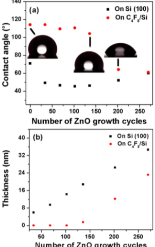
Figure 2a shows the variation in contact angle of Si(100) and fluorocarbon/Si surfaces with the increase in ZnO ALD growth cycles. The contact angle of barefluorocarbon/Si was measured as 114° which indicates the hydrophobic nature of grown polymerfilm. On the other hand, contact angle of bare Si(100) was measured as 71°. The contact angle of fluorocarbon/Si film does not change noticeably until 136 growth cycles of ZnO. After 102 growth cycles of ZnO on fluorocarbon/Si(100), contact angle was measured as 110.5° which decreases to 104.2° after 136-cycle growth. This slight decrease of contact angle suggests the onset of ZnO nucleation onfluorocarbon/Si after 136 cycles of ZnO growth. With further increase in growth cycles from 136 to 202, the contact angle decreases remarkably and falls down to 64°. This result shows that ZnO growth initiates around 136 ALD cycles due to degradation of the hydrophobic nature of fluorocarbon polymer layer. On the contrary, the contact angle of Si surface changes from 71° to 49° when exposed to 34 cycles of ZnO growth and remains stable until 202 growth cycles where it exhibits a slight increase. Figure 2b shows the change in ZnO thickness with the increase
Figure 1.(a) XPS survey scan obtained from a∼32 nm thick plasma polymerized fluorocarbon thin film deposited on Si(100). High resolution XPS scans of (b) F 1s and (c) C 1s obtained from the same film.
in number of growth cycles on Si(100) and fluorocarbon/Si. Thickness of ZnO increases linearly after nucleation onset with the increase in number of growth cycles which is typically observed for ALD processes. The growth per cycle (GPC) of ZnO on Si(100) is measured as∼1.3−1.4 Å. On fluorocarbon/ Si, no growth of ZnO is observed until 102 ALD cycles while a very thin layer of∼1.5 nm ZnO was measured after the 136th cycle. With further increase in growth cycles, the growth rate of ZnO onfluorocarbon/Si becomes similar as on bare Si(100). The ellipsometer measurements are consistent with the contact angle measurements, which confirms ZnO growth inhibition on fluorocarbon/Si(100) up to 102 ALD growth cycles.
To confirm the ZnO blocking ability of plasma polymerized fluorocarbon layer, XPS measurements (Figure 3) were conducted on Si(100) andfluorocarbon/Si substrates exposed with different number of ALD cycles. Survey scans from the surface of ZnO films grown on Si(100) (Figure 3a) indicated the presence of zinc, oxygen, and carbon with Zn 2p3, O 1s, and C 1s peaks, respectively. ZnO samples with different number of ALD cycles on Si(100) reveal the same peaks of Zn 2p3, O 1s, and C 1s.Figure 3b shows the XPS survey scans obtained fromfluorocarbon coated substrates exposed to ALD growth cycles starting from 34 up to 270. Only F 1s and C 1s peaks are observed until 102 growth cycles which are originating from the plasma polymerized fluorocarbon layer. Although no Zn signal was observed up to 102 cycles, a small Zn signal appeared at 136 cycles confirming the initiation of ZnO growth on fluorocarbon/Si. A meaningful Zn 2p3 peak begins to appear with 202 ALD cycles and remains stable for further growth cycles. The fact that F 1s peak disappears abruptly after 136 ZnO ALD cycles supports the nucleation onset.
These results further verify the contact angle and ellipsometer measurements and show that ZnO growth initiates
around 136 ALD cycles and that plasma polymerized fluorocarbon layer is effectively blocking ZnO growth up to ∼130 ALD cycles. Table 1 provides a direct comparison of
atomic percentages (at. %) of Zn from ZnO grown on Si(100) andfluorocarbon/Si which are evaluated from the quantifica-tion of XPS survey scans. A notable rise in Zn at. % is observed only after 136 ZnO ALD growth cycles onfluorocarbon/Si. Zn at. % remains steady at a value around∼36−37 at. % on ZnO/ Si with zinc to oxygen ratio (Zn/O) of∼0.86−0.88.
High resolution XPS scans of Zn 2p3/2 state have been acquired to extract the formed bonding configuration and verification of XPS survey scans.Figure 4shows the HR-XPS Zn 2p3/2 scans obtained from ZnO grown onfluorocarbon/Si with different number of growth cycles. No clear peak is observed for Zn 2p3/2scan up to 102 ALD cycles, while a weak and rather broad peak is observed for 136 growth cycles of ZnO onfluorocarbon/Si. There is a drastic increase in Zn 2p3/2peak intensity as the number of growth cycles reach 202. Indeed a clear well-established Zn 2p3/2 peak is observed at 202nd and 270th ALD cycles onfluorocarbon/Si. This peak is observed at a binding energy value of 1022.12 eV and corresponds to the
Figure 2.Variation in contact angle (a) and thickness (b) of ZnO with the increase in number of growth cycles on Si(100) andfluorocarbon/ Si.
Figure 3.XPS survey scans of ZnO grown with different number of ALD cycles on (a) Si(100) and (b)fluorocarbon/Si revealing presence of different elements.
Table 1. Variation in Zn at. % with the Increase in Number of ZnO Growth Cycles on Si(100) and Fluorocarbon/Si
no. of growth cycles Zn at. % onfluorocarbon/Si Zn at. % on Si(100)
34 − 31.28 68 − 24.2 102 − 36.3 136 1.62 37.02 202 24.72 37.54 270 37.58 37.89
Zn−O bond.69These results show excellent correlation with all the characterization results provided so far.
SEM imaging was performed to observe the surface morphology of ZnO grown on Si and fluorocarbon/Si. Parts a and b of Figure S1 show the SEM images of bare fluorocarbon/Si and ZnO grown on fluorocarbon/Si with 68 number of growth cycles, respectively. These SEM images reveal the uniform surface morphology of fluorocarbon layer and illustrate no observable growth of ZnO onfluorocarbon/Si after 68 growth cycles. Parts a and b ofFigure 5show the SEM
images of ZnO grown with 102 cycles of growth on fluorocarbon/Si and Si(100), respectively. Very few ZnO nuclei begin to form on fluorocarbon/Si surface after 102 ALD cycles, while the grainy structure of ZnO is clearly visible on Si(100) with the same number of ZnO growth cycles. As XPS did not detect any ZnO on fluorocarbon/Si up to 102 cycles, the observed ZnO nuclei might possibly be below the detection limit of XPS. Parts c and d ofFigure 5show the SEM images of 136-cycle ZnO on fluorocarbon/Si and Si. The quantity of ZnO nuclei notably increased after 136 growth cycles on fluorocarbon/Si with significantly larger areal coverage, while relatively larger grains are observed on its
counterpart ZnO on Si(100). On the basis of contact angle, spectroscopic ellipsometer, XPS, and SEM measurements presented above, we conclude that plasma-polymerized fluorocarbon layer is effective in blocking ZnO growth up to more than 100 ALD cycles.
We have also investigated the blocking/inhibition ability of plasma-polymerized fluorocarbon layer against other metal oxide materials including HfO2 and Al2O3. HfO2 and Al2O3 growth have been performed in the same reactor with thermal ALD using various number of ALD cycles on plasma polymerized fluorocarbon layer coated on Si(100) and on bare Si(100) substrates. Contact angle, spectroscopic ellips-ometer, and XPS measurements have similarly been performed to investigate the HfO2and Al2O3growth selectivity on plasma polymerized fluorocarbon layer. Figure 6 shows the contact
angle and thickness variation of ALD grown HfO2 on fluorocarbon/Si(100) and Si(100) as a function of total number of growth cycles. Both Si(100) and fluorocarbon/Si show an abrupt decrease in contact angle (Figure 6a) after 50 cycles of HfO2 growth. A slight increase in contact angle is observed for 100 cycles of HfO2 growth on Si(100) and fluorocarbon/Si and then it becomes nearly constant for both the substrates. Figure 6b shows change in thickness of ALD grown HfO2onfluorocarbon/Si and Si(100) with the increase in number of growth cycles. The thickness of HfO2on Si(100) increases linearly with the increase in number of growth cycles and the GPC is measured as∼0.95−1.00 Å. On the other hand, the growth rate of HfO2is substantially less onfluorocarbon/Si in thefirst 100 cycles of growth in contrast with Si(100). With the increase in number of cycles beyond 100, GPC of HfO2on fluorocarbon/Si becomes similar as on Si(100). It is evident from Figure 6b that the slope of HfO2 thickness increase (GPC) on fluorocarbon/Si is less up to 100 cycles while it
Figure 4.HR-XPS scans of Zn 2p3/2obtained from ZnO grown on fluorocarbon/Si as a function of ALD growth cycles.
Figure 5.Plan view SEM images of 102 cycles ALD grown ZnO on (a)fluorocarbon/Si and (b) Si(100); 136 cycles ALD grown ZnO on (c)fluorocarbon/Si and (d) Si(100) (all scale bars = 50 nm).
Figure 6.Variation in (a) contact angle and (b) thickness of HfO2as a function of ALD growth cycles on Si(100) andfluorocarbon/Si. The Journal of Physical Chemistry C
increases beyond that and becomes same as GPC on Si(100). These results reveal that initial nucleation of HfO2 is considerably slower on fluorocarbon/Si up to 100 cycles, where GPC equals the GPC on bare Si surface after sufficient coverage of HfO2is achieved.
XPS measurements are conducted on HfO2 grown on Si(100) and fluorocarbon/Si(100) and recorded survey scans are presented inFigure S2, parts a and b, which indicate the presence of Hf 4f, C 1s, and O 1s peaks from HfO2grown on both substrate surfaces. However, peak intensity of Hf 4f obtained from HfO2grown with 50 cycles on fluorocarbon/Si is notably lower than the corresponding peak seen on Si(100) with same number of growth cycles.
Atomic percentages obtained from quantification of these survey scans are provided inTable S1. These results verify the contact angle and ellipsometer measurements results and confirm that HfO2 nucleation is relatively slower on fluorocarbon/Si within the initial growth cycles.
A similar set of experiments have been conducted for Al2O3 grown on fluorocarbon/Si and Si(100). Figure 7 shows the
variation of contact angle and thickness with the number of ALD growth cycles on both substrates. In contrary to ZnO and HfO2, an immediate sharp decrease in contact angle has been observed for Al2O3 on both fluorocarbon/Si and Si(100), stabilizing at a value of∼37−45°. A direct relation in alumina thickness and number of ALD cycles can be noticed from Figure 7b with an alumina GPC slightly less onfluorocarbon/Si then on Si(100). XPS measurements have been conducted on Al2O3grown onfluorocarbon/Si and Si(100) and survey scans have been presented inFigure S3, parts a and b. Al 2p, C 1s, and O 1s peaks have been observed fromfilms grown on both substrates. Al quantification from these survey scans have been
presented inTable S2, which shows a significant presence of Al on all the substrates. These results support the observations of contact angle and spectroscopic ellipsometer measurements and reveal that the plasma-polymerized fluorocarbon layer is rather ineffective in blocking alumina growth. It has been observed that blocking ability of a particular layer for successful AS-ALD might depend on ALD processing conditions such as precursor employed, working pressure, purge time, and substrate temperature.10,29,52,70−72 In addition to ALD processing conditions, blocking capability of thefluorocarbon layer may also depend on plasma polymerization conditions such as plasma energy, working pressure, andflow rate of feed gas. Although the plasma-polymerizedfluorocarbon layer shows a superior growth blocking/inhibition feature for the ZnO ALD process, it may further be optimized along with ALD process conditions in order to achieve growth selectivity for HfO2and Al2O3 as well. Moreover, the achieved maximum number of ALD cycles before ZnO nucleation takes over might be further extended with a systematic study in which ICP polymerization and ALD process conditions are optimized.
After demonstrating the ability of plasma polymerized fluorocarbon layer to inhibit ZnO ALD growth, the next step was to employfluorocarbon layer for patterning of ALD grown ZnO. Photolithography was used to prepare bare Si and fluorocarbon/Si checkerboard and line pattern structures in a sequential manner.Figure 8a shows a plan-view SEM image of 102 cycle ZnO ALD grown onfluorocarbon layer line patterns. The darker squares represent the areas where fluorocarbon layer is present, while bright areas represent the ZnO grown surface. Inset ofFigure 8a shows the HR-SEM image from the interface of dark and bright areas, which reveals the grainy structure of ZnO only fromfluorocarbon uncoated area while negligible ZnO grains were observed on fluorocarbon layer. Similarly,Figure 8b shows a plan-view SEM image of 102 cycle ZnO ALD grown onfluorocarbon checkerboard patterns. The HR-SEM image obtained from the interface of coated and uncoated fluorocarbon regions reveal that grainy structure of ZnO is only present on the bare Si region.
XPS line scan was performed on a 2 mm wide ZnO-coated patternedfluorocarbon/Si lines. The minimum spot size of X-rays that could be utilized was∼100 μm; therefore, patterned lines of 2 mm width were selected for analysis in order to gather the data from various points. A line across an area of interest is selected on the sample and the XPS gathered data along the line at various points. Zn 2p intensity was measured in terms of counts per second vs spatial location along the line and presented inFigure 8c. Clearly, the higher intensity of the Zn 2p peak is only observed at the location of the ZnO pattern while the intensity at other points was equal to background intensity, confirming the successful pattern placement of ZnO.
■
SUMMARY AND CONCLUSIONWe demonstrate a method for achieving area-selective ALD using ICP polymerized fluorocarbon layer as a hydrophobic blocking layer to inhibit ALD growth. Contact angle, spectroscopic ellipsometry, XPS, and SEM measurements were used to evaluate the capability of plasma polymerized fluorocarbon layer to inhibit metal-oxide ALD growth. Characterizations carried out revealed that effective ZnO blocking on fluorocarbon layer can be achieved up to more than 100 ALD cycles, resulting in selective growth of∼15 nm thickfilms. Initial nucleation has been observed for 136-cycle ZnOfilms and additional ALD cycles eventually led to growth
Figure 7.Variation in (a) contact angle and (b) thickness of Al2O3 with the increase in number of growth cycles on Si(100) and fluorocarbon/Si.
on fluorocarbon layer at conventional GPC values. On the other hand, although no complete blocking is observed, a rather slow nucleation has been observed for HfO2 growth on fluorocarbon coated surfaces up to 100 growth cycles, while the same blocking layer deposited under the present conditions has been found to be ineffective in blocking Al2O3 growth. By exploiting this inhibition feature of fluorocarbon layer, self-aligned ZnO deposition has been performed on lithographically defined patterned fluorocarbon/Si sample. High-resolution SEM images and XPS line scans confirmed the successful patterning of ZnO up to a film thickness of ∼15 nm. The robust albeit rather simple and straightforward technique presented in this work overcomes various challenges associated with previous methods of AS-ALD and provides an alternative route toward nanopatterning using AS-ALD. Moreover, this
method is expected to be implemented in achieving AS-ALD of other materials as well including metals and III−V compounds.
■
ASSOCIATED CONTENT*
S Supporting InformationThe Supporting Information is available free of charge on the ACS Publications websiteat DOI:10.1021/acs.jpcc.6b09406.
SEM images of bare fluorocarbon/Si sample and ZnO coated onfluorocarbon/Si sample with 68 cycles and, in addition, XPS survey scans of HfO2 and Al2O3 grown with different number of growth cycles on Si(100) and on fluorocarbon/Si with the quantification of hafnium and aluminum atomic percentages (PDF)
■
AUTHOR INFORMATIONCorresponding Authors
*(A.H.) E-mail:[email protected]. *(N.B.) E-mail:[email protected].
Author Contributions
The manuscript was written through contributions of all authors. All authors have given approval to thefinal version of the manuscript.
Notes
The authors declare no competingfinancial interest.
■
ACKNOWLEDGMENTSThe authors acknowledge the National Nanotechnology Research Center (UNAM), Bilkent University for providing the growth and materials characterization facilities. Authors also acknowledge Mr. Murat Serhatlioglu from UNAM for drawing the table of content artwork.
■
REFERENCES(1) Zhang, P.; Mayer, T. S.; Jackson, T. N. 2007 IEEE Device Research Conference: Tour de Force Multigate and Nanowire Metal Oxide Semiconductor Field-Effect Transistors and Their Application. ACS Nano 2007, 1, 6−9.
(2) Biercuk, M. J.; Monsma, D. J.; Marcus, C. M.; Becker, J. S.; Gordon, R. G. Low-Temperature Atomic-Layer-Deposition Lift-off Method for Microelectronic and Nanoelectronic Applications. Appl. Phys. Lett. 2003, 83, 2405.
(3) Goldberger, J.; Hochbaum, A. I.; Fan, R.; Yang, P. Silicon Vertically Integrated Nanowire Field Effect Transistors. Nano Lett. 2006, 6, 973−977.
(4) Kim, J. M.; Lee, H. B. R.; Lansalot, C.; Dussarrat, C.; Gatineau, J.; Kim, H. Plasma-Enhanced Atomic Layer Deposition of Cobalt Using Cyclopentadienyl Isopropyl Acetamidinato-Cobalt as a Precursor. Jpn. J. Appl. Phys. 2010, 49, 05FA10.
(5) Minaye Hashemi, F. S.; Prasittichai, C.; Bent, S. F. Self-Correcting Process for High Quality Patterning by Atomic Layer Deposition. ACS Nano 2015, 9, 8710−8717.
(6) Gay, G.; Baron, T.; Agraffeil, C.; Salhi, B.; Chevolleau, T.; Cunge, G.; Grampeix, H.; Tortai, J.-H.; Martin, F.; Jalaguier, E.; et al. CMOS Compatible Strategy Based on Selective Atomic Layer Deposition of a Hard Mask for Transferring Block Copolymer Lithography Patterns. Nanotechnology 2010, 21, 435301.
(7) Hashemi, F. S. M.; Prasittichai, C.; Bent, S. F. A New Resist for Area Selective Atomic and Molecular Layer Deposition on Metal-Dielectric Patterns. J. Phys. Chem. C 2014, 118, 10957−10962.
(8) Lee, J. P.; Sung, M. M. A New Patterning Method Using Photocatalytic Lithography and Selective Atomic Layer Deposition. J. Am. Chem. Soc. 2004, 126, 28−29.
Figure 8.(a) Plan-view SEM image of 102 cycle ZnO ALD grown on fluorocarbon line patterns (scale bar = 10 μm) (inset) HR-SEM image from the interface of ZnO andfluorocarbon layer (scale bar = 50 nm). (b) Plan-view SEM image of 102 cycle ZnO ALD grown on fluorocarbon checker board patterns (scale bar = 150 μm) (inset) HR-SEM image from the interface of ZnO andfluorocarbon layer (scale bar = 100 nm). (c) XPS line scan obtained from patterned ZnO substrate.
(9) Chen, R.; Bent, S. F. Chemistry for Positive Pattern Transfer Using Area-Selective Atomic Layer Deposition. Adv. Mater. 2006, 18, 1086−1090.
(10) Mackus, A. J. M.; Bol, A. A.; Kessels, W. M. M. The Use of Atomic Layer Deposition in Advanced Nanopatterning. Nanoscale 2014, 6, 10941−10960.
(11) Profijt, H. B.; Potts, S. E.; van de Sanden, M. C. M.; Kessels, W. M. M. Plasma-Assisted Atomic Layer Deposition: Basics, Oppor-tunities, and Challenges. J. Vac. Sci. Technol., A 2011, 29, 050801.
(12) Puurunen, R. L. Surface Chemistry of Atomic Layer Deposition: A Case Study for the Trimethylaluminum/water Process. J. Appl. Phys. 2005, 97, 121301.
(13) George, S. M. Atomic Layer Deposition: An Overview. Chem. Rev. 2010, 110, 111−131.
(14) Atanasov, S. E.; Kalanyan, B.; Parsons, G. N. Inherent Substrate-Dependent Growth Initiation and Selective-Area Atomic Layer Deposition of TiO2Using“water-Free” Metal-Halide/metal Alkoxide Reactants. J. Vac. Sci. Technol., A 2016, 34, 01A148.
(15) Kalanyan, B.; Lemaire, P. C.; Atanasov, S. E.; Ritz, M. J.; Parsons, G. N. Using Hydrogen to Expand the Inherent Substrate Selectivity Window during Tungsten Atomic Layer Deposition. Chem. Mater. 2016, 28, 117−126.
(16) Jiang, X.; Wang, H.; Qi, J.; Willis, B. G. In-Situ Spectroscopic Ellipsometry Study of Copper Selective-Area Atomic Layer Deposition on Palladium. J. Vac. Sci. Technol., A 2014, 32, 041513.
(17) McDonnell, S.; Longo, R. C.; Seitz, O.; Ballard, J. B.; Mordi, G.; Dick, D.; Owen, J. H. G.; Randall, J. N.; Kim, J.; Chabal, Y. J.; Cho, K.; Wallace, R. M. Controlling the Atomic Layer Deposition of Titanium Dioxide on Silicon: Dependence on Surface Termination. J. Phys. Chem. C 2013, 117, 20250−20259.
(18) Mackus, A. J. M.; Thissen, N. F. W.; Mulders, J. J. L.; Trompenaars, P. H. F.; Verheijen, M. A.; Bol, A. A.; Kessels, W. M. M. Direct-Write Atomic Layer Deposition of High-Quality Pt Nanostruc-tures: Selective Growth Conditions and Seed Layer Requirements. J. Phys. Chem. C 2013, 117, 10788−10798.
(19) Mackus, A. J. M.; Mulders, J. J. L.; van De Sanden, M. C. M.; Kessels, W. M. M. Local Deposition of High-Purity Pt Nanostructures by Combining Electron Beam Induced Deposition and Atomic Layer Deposition. J. Appl. Phys. 2010, 107, 116102.
(20) Mackus, A. J. M.; Dielissen, S. A. F.; Mulders, J. J. L.; Kessels, W. M. M. Nanopatterning by Direct-Write Atomic Layer Deposition. Nanoscale 2012, 4, 4477−4480.
(21) Gupta, R.; Willis, B. G. Nanometer Spaced Electrodes Using Selective Area Atomic Layer Deposition. Appl. Phys. Lett. 2007, 90, 253102.
(22) Färm, E.; Lindroos, S.; Ritala, M.; Leskelä, M. Microcontact Printed RuOxFilm as an Activation Layer for Selective-Area Atomic Layer Deposition of Ruthenium. Chem. Mater. 2012, 24, 275−278.
(23) Liu, J.; Mao, Y.; Lan, E.; Banatao, D. R.; Forse, G. J.; Lu, J.; Blom, H. O.; Yeates, T. O.; Dunn, B.; Chang, J. P. Generation of Oxide Nanopatterns by Combining Self-Assembly of S-Layer Proteins and Area-Selective Atomic Layer Deposition. J. Am. Chem. Soc. 2008, 130, 16908−16913.
(24) Cheng, N.; Banis, M. N.; Liu, J.; Riese, A.; Li, X.; Li, R.; Ye, S.; Knights, S.; Sun, X. Extremely Stable Platinum Nanoparticles Encapsulated in a Zirconia Nanocage by Area-Selective Atomic Layer Deposition for the Oxygen Reduction Reaction. Adv. Mater. 2015, 27, 277−281.
(25) Guo, L.; Lee, I.; Zaera, F. Patterning of Solid Films via Selective Atomic Layer Deposition Based on Silylation and UV/Ozonolysis. ACS Appl. Mater. Interfaces 2016, 8, 19836−19841.
(26) Seo, E. K.; Lee, J. W.; Sung-Suh, H. M.; Sung, M. M. Atomic Layer Deposition of Titanium Oxide on Self-Assembled-Monolayer-Coated Gold. Chem. Mater. 2004, 16, 1878−1883.
(27) Kim, W.-H.; Lee, H.-B.-R.; Heo, K.; Lee, Y. K.; Chung, T.-M.; Kim, C. G.; Hong, S.; Heo, J.; Kim, H. Atomic Layer Deposition of Ni Thin Films and Application to Area-Selective Deposition. J. Electro-chem. Soc. 2011, 158, D1−D5.
(28) Park, K. J.; Doub, J. M.; Gougousi, T.; Parsons, G. N. Microcontact Patterning of Ruthenium Gate Electrodes by Selective Area Atomic Layer Deposition. Appl. Phys. Lett. 2005, 86, 051903.
(29) Färm, E.; Kemell, M.; Ritala, M.; Leskela, M. Selective-Area Atomic Layer Deposition Using Poly (Methyl Methacrylate) Films as Mask Layers. J. Phys. Chem. C 2008, 112, 15791−15795.
(30) Park, M. H.; Jang, Y. J.; Sung-Suh, H. M.; Sung, M. M. Selective Atomic Layer Deposition of Titanium Oxide on Patterned Self-Assembled Monolayers Formed by Microcontact Printing. Langmuir 2004, 20, 2257−2260.
(31) Hua, Y.; King, W. P.; Henderson, C. L. Nanopatterning Materials Using Area Selective Atomic Layer Deposition in Conjunction with Thermochemical Surface Modification via Heated AFM Cantilever Probe Lithography. Microelectron. Eng. 2008, 85, 934−936.
(32) Guo, L.; Qin, X.; Zaera, F. Chemical Treatment of Low-K Dielectric Surfaces for Patterning of Thin Solid Films in Micro-electronic Applications. ACS Appl. Mater. Interfaces 2016, 8, 6293− 6300.
(33) Zhang, W.; Engstrom, J. R. Effect of Substrate Composition on Atomic Layer Deposition Using Self-Assembled Monolayers as Blocking Layers. J. Vac. Sci. Technol., A 2016, 34, 01A107.
(34) Hashemi, F. S. M.; Bent, S. F. Sequential Regeneration of Self-Assembled Monolayers for Highly Selective Atomic Layer Deposition. Adv. Mater. Interfaces 2016, 1600464.
(35) Vervuurt, R. H. J.; Sharma, A.; Jiao, Y.; Kessels, W.; Bol, A. A. Area-Selective Atomic Layer Deposition of Platinum Using Photo-sensitive Polyimide. Nanotechnology 2016, 27, 405302.
(36) Huang, J.; Lee, M.; Lucero, A.; Cheng, L.; Kim, J. Area-Selective ALD of TiO2 Nanolines with Electron-Beam Lithography. J. Phys. Chem. C 2014, 118, 23306−23312.
(37) Bent, S. F. Heads or Tails: Which Is More Important in Molecular Self-Assembly? ACS Nano 2007, 1, 10−12.
(38) Färm, E.; Kemell, M.; Ritala, M.; Leskelä, M. Selective-Area Atomic Layer Deposition with Microcontact Printed Self-Assembled Octadecyltrichlorosilane Monolayers as Mask Layers. Thin Solid Films 2008, 517, 972−975.
(39) Huang, J.; Lee, M.; Kim, J. Selective Atomic Layer Deposition with Electron-Beam Patterned Self-Assembled Monolayers. J. Vac. Sci. Technol., A 2012, 30, 01A128.
(40) Yan, M.; Koide, Y.; Babcock, J. R.; Markworth, P. R.; Belot, J. a.; Marks, T. J.; Chang, R. P. H. Selective-Area Atomic Layer Epitaxy Growth of ZnO Features on Soft Lithography-Patterned Substrates. Appl. Phys. Lett. 2001, 79, 1709−1711.
(41) Lee, W.; Prinz, F. B. Area-Selective Atomic Layer Deposition Using Self-Assembled Monolayer and Scanning Probe Lithography. J. Electrochem. Soc. 2009, 156, G125−G128.
(42) Jiang, X.; Chen, R.; Bent, S. F. Spatial Control over Atomic Layer Deposition Using Microcontact-Printed Resists. Surf. Coat. Technol. 2007, 201, 8799−8807.
(43) Chen, R.; Kim, H.; McIntyre, P. C.; Porter, D. W.; Bent, S. F. Achieving Area-Selective Atomic Layer Deposition on Patterned Substrates by Selective Surface Modification. Appl. Phys. Lett. 2005, 86, 191910.
(44) Lee, W.; Dasgupta, N. P.; Trejo, O.; Lee, J. R.; Hwang, J.; Usui, T.; Prinz, F. B. Area-Selective Atomic Layer Deposition of Lead Sulfide: Nanoscale Patterning and DFT Simulations. Langmuir 2010, 26, 6845−6852.
(45) Lee, H.-B.-R.; Kim, W.-H.; Lee, J. W.; Kim, J.-M.; Heo, K.; Hwang, I. C.; Park, Y.; Hong, S.; Kim, H. High Quality Area-Selective Atomic Layer Deposition Co Using Ammonia Gas as a Reactant. J. Electrochem. Soc. 2010, 157, D10−D15.
(46) Färm, E.; Vehkamäki, M.; Ritala, M.; Leskelä, M. Passivation of Copper Surfaces for Selective-Area ALD Using a Thiol Self-Assembled Monolayer. Semicond. Sci. Technol. 2012, 27, 074004.
(47) Färm, E.; Kemell, M.; Ritala, M.; Leskelä, M. Self-Assembled Octadecyltrimethoxysilane Monolayers Enabling Selective-Area Atomic Layer Deposition of Iridium. Chem. Vap. Deposition 2006, 12, 415−417.
(48) Cao, K.; Zhu, Q.; Shan, B.; Chen, R. Controlled Synthesis of Pd/Pt Core Shell Nanoparticles Using Area-Selective Atomic Layer Deposition. Sci. Rep. 2015, 5, 8470.
(49) Jiang, X.; Bent, S. F. Area-Selective Atomic Layer Deposition of Platinum on YSZ Substrates Using Microcontact Printed SAMs. J. Electrochem. Soc. 2007, 154, D648−D656.
(50) Chalker, P. R.; Marshall, P. A.; Dawson, K.; Brunell, I. F.; Sutcliffe, C. J.; Potter, R. J. Vacuum Ultraviolet Photochemical Selective Area Atomic Layer Deposition of Al2O3Dielectrics. AIP Adv. 2015, 5, 017115.
(51) Kim, W.-H.; Minaye Hashemi, F. S.; Mackus, A. J. M.; Singh, J.; Kim, Y.; Bobb-Semple, D.; Fan, Y.; Kaufman-Osborn, T.; Godet, L.; Bent, S. F. A Process for Topographically Selective Deposition on 3D Nanostructures by Ion Implantation. ACS Nano 2016, 10, 4451−4458. (52) Sinha, A.; Hess, D. W.; Henderson, C. L. Area Selective Atomic Layer Deposition of Titanium Dioxide: Effect of Precursor Chemistry. J. Vac. Sci. Technol. B 2006, 24, 2523−2532.
(53) Coll, M.; Palau, A.; Gonzalez-Rosillo, J. C.; Gazquez, J.; Obradors, X.; Puig, T. Integration of Atomic Layer Deposition CeO2 Thin Films with Functional Complex Oxides and 3D Patterns. Thin Solid Films 2014, 553, 7−12.
(54) Ellinger, C. R.; Nelson, S. F. Selective Area Spatial Atomic Layer Deposition of ZnO, Al2O3, and Aluminum-Doped ZnO Using Poly(vinyl Pyrrolidone). Chem. Mater. 2014, 26, 1514−1522.
(55) Levy, D. H.; Ellinger, C. R.; Nelson, S. F. Metal-Oxide Thin-Film Transistors Patterned by Printing. Appl. Phys. Lett. 2013, 103, 043505.
(56) Färm, E.; Kemell, M.; Santala, E.; Ritala, M.; Leskelä, M. Selective-Area Atomic Layer Deposition Using Poly(vinyl Pyrroli-done) as a Passivation Layer. J. Electrochem. Soc. 2010, 157, K10−K-14. (57) Park, K. J.; Parsons, G. N. Selective Area Atomic Layer Deposition of Rhodium and Effective Work Function Characterization in Capacitor Structures. Appl. Phys. Lett. 2006, 89, 043111.
(58) Mullings, M. N.; Lee, H.-B.-R.; Marchack, N.; Jiang, X.; Chen, Z.; Gorlin, Y.; Lin, K.-P.; Bent, S. F. Area Selective Atomic Layer Deposition by Microcontact Printing with a Water-Soluble Polymer. J. Electrochem. Soc. 2010, 157, D600−D604.
(59) Biercuk, M. J.; Monsma, D. J.; Marcus, C. M.; Becker, J. S.; Gordon, R. G. Low-Temperature Atomic-Layer-Deposition Lift-off Method for Microelectronic and Nanoelectronic Applications. Appl. Phys. Lett. 2003, 83, 2405−2407.
(60) Sinha, A.; Hess, D. W.; Henderson, C. L. Area-Selective ALD of Titanium Dioxide Using Lithographically Defined Poly(methyl Methacrylate) Films. J. Electrochem. Soc. 2006, 153, G465−G469.
(61) Suresh, V.; Huang, M. S.; Srinivasan, M. P.; Guan, C.; Fan, H. J.; Krishnamoorthy, S. Robust, High-Density Zinc Oxide Nanoarrays by Nanoimprint Lithography-Assisted Area-Selective Atomic Layer Deposition. J. Phys. Chem. C 2012, 116, 23729−23734.
(62) Levy, D. H.; Nelson, S. F.; Freeman, D. Oxide Electronics by Spatial Atomic Layer Deposition. J. Disp. Technol. 2009, 5, 484−494. (63) Coll, M.; Gazquez, J.; Palau, A.; Varela, M.; Obradors, X.; Puig, T. Low Temperature Epitaxial Oxide Ultrathin Films andNanos-tructures by Atomic Layer Deposition. Chem. Mater. 2012, 24, 3732− 3737.
(64) Dandley, E. C.; Lemaire, P. C.; Zhu, Z.; Yoon, A.; Sheet, L.; Parsons, G. N. Wafer-Scale Selective-Area Deposition of Nanoscale Metal Oxide Features Using Vapor Saturation into Patterned Poly(methyl Methacrylate) Templates. Adv. Mater. Interfaces 2016, 3, 1500431.
(65) Avila, J. R.; Emery, J. D.; Pellin, M. J.; Martinson, A. B. F.; Farha, O. K.; Hupp, J. T. Porphyrins as Templates for Site-Selective Atomic Layer Deposition: Vapor Metalation and in Situ Monitoring of Island Growth. ACS Appl. Mater. Interfaces 2016, 8, 19853−19859.
(66) Chopra, S. N.; Zhang, Z.; Kaihlanen, C.; Ekerdt, J. G. Selective Growth of Titanium Nitride on HfO2 on Surfaces with Topography. Chem. Mater. 2016, 28, 4928−4934.
(67) Yeo, L. P.; Yan, Y. H.; Lam, Y. C.; Chan-Park, M. B. Design of Experiment for Optimization of Plasma-Polymerized
Octafluorocyclo-butane Coating on Very High Aspect Ratio Silicon Molds. Langmuir 2006, 22, 10196−10203.
(68) Li, X.; Hua, X.; Ling, L.; Oehrlein, G. S.; Barela, M.; Anderson, H. M. Fluorocarbon-Based Plasma Etching of SiO: Comparison of C4F6/Ar and C4F8/Ar Discharges. J. Vac. Sci. Technol., A 2002, 20, 2052−2061.
(69) Abd Aziz, S. N. Q. A.; Pung, S.-Y.; Ramli, N. N.; Lockman, Z. Growth of ZnO Nanorods on Stainless Steel Wire Using Chemical Vapour Deposition and Their Photocatalytic Activity. Sci. World J. 2014, 2014, 252851.
(70) Avila, J. R.; Demarco, E. J.; Emery, J. D.; Farha, O. K.; Pellin, M. J.; Hupp, J. T.; Martinson, A. B. F. Real-Time Observation of Atomic Layer Deposition Inhibition: Metal Oxide Growth on Self-Assembled Alkanethiols. ACS Appl. Mater. Interfaces 2014, 6, 11891−11898.
(71) Haider, A.; Yilmaz, M.; Deminskyi, P.; Eren, H.; Biyikli, N. Nanoscale Selective Area Atomic Layer Deposition of TiO2Using E-Beam Patterned Polymers. RSC Adv. 2016, 6, 106109−106119.
(72) Vallat, R.; Gassilloud, R.; Eychenne, B.; Vallée, C. Selective Deposition of Ta2O5 by Adding Plasma Etching Super-Cycles in Plasma Enhanced Atomic Layer Deposition Steps. J. Vac. Sci. Technol., A 2017, 35, 01B104.