Differentiation of Domains in Composite Surface
Structures by Charge-Contrast X-ray Photoelectron
Spectroscopy
Sefik Suzer,*,†Aykutlu Daˆ na,‡and Gulay Ertas†
Chemistry Department and Physics Department, Bilkent University, 06800 Ankara, Turkey
An external bias is applied to two samples containing composite surface structures, while recording an XPS spectrum. Altering the polarity of the bias affects the extent of differential charging in domains that are chemi-cally or electronichemi-cally different to create a charge contrast. By utilizing this charge contrast, we show that two distinct silicon nitride and silicon oxynitride domains are present in one of the composite samples. Similarly, we use this technique to show that titanium oxide and silicon oxide domains exist as separate chemical entities in another composite sample.
X-ray photoelectron spectroscopy (XPS) is a powerful analytical technique for characterizing different chemical/physical forms of elements within the top 0-10-nm surface layers.1In principle, determination of the chemical state of an element in a homoge-neous surface is straightforward. However, in practical analysis, one is faced with having to analyze a number of composite materials that are heterogeneous from the viewpoint of micro-structure, chemical composition, or both. In general, a specimen for XPS analysis should be conductive, and in the case of composite materials, the electronic conductivity may not be uniform and differential charging may develop as a result of photoemission from insulating components. Although several techniques have been developed to minimize the charging, complete elimination is not always possible.2The positive charging is usually compensated by directed flow of low-energy electrons from an external unit (flood gun) to the sample, which under certain circumstances, overneutralizes it and may even cause negative charging.
Purposely generated negative charging, called controlled surface charging (CSC), has been successfully used for deriving some chemical/physical properties of various surface structures.3-7 Lau and co-workers have utilized the CSC to extract structural andelectricalpropertiesofultrathindielectricsonsemiconductors.8-11
Thomas et al.12were able to separate the surface spectrum (mainly silicon dioxide) from the silicon substrate spectrum (consisting of contamination and silicon dioxide on silicon), by use of surface charging, and similar applications were also reported by Ermolieff et al.13 and Bell and Joubert,14 while Miller et al. applied the technique to separate the XPS signals of the fiber from the exposed matrix at fractured surfaces.15Surface charging was also utilized for lateral differentiation of mesoscopic layers and for depth profiling.6,7 One interesting application of the surface charging for composite surface structures was reported by Ohno et al.16for separate examination of the chemical nature of the carbon fibers and the BMI resin, which enabled them to resolve the carbon fiber and the resin phases in one specimen.
In all of these studies, surface charging was controlled or varied via a low-energy electron flood gun, whereas, as we attempt to demonstrate in the present contribution, useful information can also be extracted by analysis of the positively charged surfaces. We control or enhance the positive charging by applying an external bias to the sample rod while recording the spectrum, similar to what has been reported by others.17-21We were able
* Towhomcorrespondenceshouldbeaddressed.E-mail: [email protected].
†Chemistry Department. ‡Physics Department.
(1) Briggs, D.; Seah, M. P. Practical surface analysis. Part I. Auger and X-ray photoelectron spectroscopy,2 nd ed.; John Wiley & Sons Ltd.: London, England, 1996.
(2) Cazaux, J. J. Electron Spectrosc. Relat. Phenom. 2000, 113, 15-33. (3) Sherwood, P. M. A. Surf. Sci. 2006, 600, 771-772.
(4) Lau, W. M.; Wu, X. W. Surf. Sci. 1991, 245, 345-352. (5) Lau, W. M. J. Appl. Phys. 1989, 65, 2047-2052.
(6) Shabtai, K.; Rubinstein, I.; Cohen, S. R.; Cohen, H. J. Am. Chem. Soc. 2000, 122, 4959-4962.
(7) Doron-Mor, H.; Hatzor, A.; Vaskevich, A.; van der Boom-Moav, T.; Shanzer, A.; Rubinstein, I.; Cohen, H. Nature 2000, 406, 382-385.
(8) Lau, W. M. Appl. Phys. Lett. 1989, 54, 338-340.
(9) Chan, R. W. M.; Kwok, R. W. M.; Lau, W. M.; Yan, H.; Wong, S. P. J. Vac. Sci. Technol., A1997, 15, 2787-2792.
(10) Chan, R. W. M.; Kwok, R. W. M.; Lau, W. M. J. Appl. Phys. 1996, 79, 3635-3639.
(11) Lau, W. M.; Jin, S.; Wu, X.-W.; Ingrey, S. J. Vac. Sci. Technol., B 1990, 8, 848-855.
(12) Thomas, J. H., III; Bryson, C. E., III; Pampalone, T. R. J. Vac. Sci. Technol., B1988, 6, 1081-1086.
(13) Ermolieff, A.; Deleonibus, S.; Marthon, S.; Blanchard, B.; Piaguet, J. J. Electron Spectrosc. Relat. Phenom.1994, 67, 409-416.
(14) Bell, F. H.; Joubert, O. J. Vac. Sci. Technol., B 1997, 15, 88-97. (15) Miller, J. D.; Harris, W. C.; Zajac, W. G. Surf. Interface Anal. 1993, 20,
977-983.
(16) Ohno, S.; Lee, M. H.; Lin, K. Y.; Ohuchi, F. S. J. Vac. Sci. Technol., A 2001, 19, 1116-1120.
(17) Gouzman, I.; Dubey, M.; Carolus, M. D.; Schwartz, J.; Bernasek, S. L. Surf. Sci.2006, 600, 773-781.
(18) Dubey, M.; Gouzman, I.; Bernasek, S. L.; Schwartz, J. Langmuir 2006, 22, 4649-4653.
(19) Johansson, G.; Hedman, J.; Berndtsson, A.; Klasson, M.; Nilsson, R. J. Electron Spectrosc. Relat. Phenom.1973, 2, 295-317.
(20) Dickinson, T.; Povey, A. F.; Sherwood, P. M. A. J. Electron Spectrosc. Relat. Phenom.1973, 2, 441-447.
(21) Havercroft, N. J.; Sherwood, P. M. A. Surf. Interface Anal. 2000, 29, 232-240.
Anal. Chem.2007,79,183-186
10.1021/ac0613683 CCC: $37.00 © 2007 American Chemical Society Analytical Chemistry, Vol. 79, No. 1, January 1, 2007 183 Published on Web 11/16/2006
to apply this simple method (i) to analyze some dielectrical properties of ultrathin silicon oxide layers, (ii) to separate otherwise overlapping XPS peaks of the same atom belonging to different chemical entities, and (iii) to derive information related to the proximity of the atoms within composite multilayers.22-24 We now extend our application to detect the presence of domains that are chemically or electronically different in different composite surface structures. For the first application, analysis of an annealed silicon oxynitride sample is presented, and for the second one, a sample containing both silicon oxide and titanium oxide is presented.
Silicon nitride has received a great deal of attention due to its superior mechanical and electrical properties for applications in microelectronics and optoelectronics. Some of these properties include better breakdown strength, higher electrical permittivity, improved barrier to impurity diffusion, and superior resistance to plasma and radiation damage.25-29However, most preparation routes produce oxynitrides rather than the pure nitride. Then, the question arises as to whether oxides and nitrides are separate entities or domains, especially after thermal annealing. Distin-guishing the various chemical domains present in a given sample is an analytical challenge, and partial success has been achieved by IR spectroscopy.30,31In both XPS and IR techniques, an average structure of the sample examined is determined, and the
pres-ence/absence of domains with different chemical compositions cannot be verified easily. Due to the predominantly amorphous nature of the oxynitride structures, diffraction techniques cannot be of help either.
Titanium and silicon mixed oxides are encountered in various catalytical and photocatalytical applications, antireflection coatings, filters, mirrors, etc.; and similar questions related to domains are also of importance.32-36For some coating applications, control of the refractive index is the most crucial issue, and two approaches have been used in order to get intermediate refractive indices: (i) use mixed oxides with a high and low index material,37,38and (ii) stack very thin layers of pure materials to achieve any index profile.39These two methods require good control of the formation of mixed material or of interfaces, and it is important to know how the interfaces are formed. Using a combination of XPS and FT-IR techniques, the formation of SisOsTi bond or SiO2/TiO2 in a single phase material depending on the Ti content in the mixture was claimed by different groups.33,38,40,41 In all these studies, separate phases were only identified by the behavior of the O 1s core level peak to indicate that at least two phases coexist. The appearance of an extra shoulder in the O 1s spectra of the
(22) Ulgut, B.; Suzer, S. J. Phys. Chem. B 2003, 107, 2939-2943. (23) Suzer, S. Anal. Chem. 2003, 75, 7026-7029.
(24) Karadas, F.; Ertas, G.; Suzer, S. J. Phys. Chem. B 2004, 108, 1515-1518. (25) Chaiyasena, I. A.; Lenahan, P. M.; Dunn, G. J. Appl. Phys. Lett. 1991, 58,
2141-2143.
(26) Bustillo, J.; Chang, C.; Haddad, S.; Wang, A. Appl. Phys. Lett. 1991, 58, 1872-1874.
(27) Dunn, G. J. J. Appl. Phys. 1989, 65, 4879-4883. (28) Dunn, G. J. Appl. Phys. Lett. 1988, 53, 1650-1651.
(29) Yount, J. T.; Lenahan, P. M.; Krick, J. T. J. Appl. Phys. 1994, 76, 1754-1758.
(30) Hernandez, M. J.; Garrido, J.; Martinez, J.; Piqueras, J. Semicond. Sci. Technol.1997, 12, 927-932.
(31) Zhang, B. R.; Yu, Z.; Collins, G. J.; Hwang, T.; Ritchie, W. H. J. Vac. Sci. Technol., A1989, 7, 176-188.
(32) Gracia, F.; Holgado, J. P.; Caballero, A.; Gonzalez-Elipe, A. R. J. Phys. Chem. B2004, 108, 17466-17476.
(33) Gracia, F.; Yubero, F.; Espinos, J. P.; Holgado, J. P.; Gonzalez-Elipe, A. R.; Girardeau, T. Surf. Interface Anal. 2006, 38, 752-756.
(34) Mergel, D.; Buschendorfa, D.; Eggerta, S.; Grammesb, R.; Samsetc, B. Thin Solid Films2000, 371, 218-224.
(35) Gracia, F.; Holgada, J. P.; Gonzalez-Elipe, A. R. Langmuir 2004, 20, 1688-1697.
(36) Abad, J.; Rogero, C.; Mendez, J.; Lopez, M. F.; Martin-Gago, J. A.; Roman, E. Appl. Surf. Sci. 2004, 234, 497-502.
(37) Demiryont, H. Appl. Opt. 1985, 24, 2647-2650.
(38) Gallas, B.; Brunet-Bruneau, A.; Fisson, S.; Vuye, G.; Rivory, J. J. Appl. Phys. 2002, 92, 1922-1928.
(39) Gluck, N. S.; Sankur, H.; Heuer, J.; DeNatale, J.; Gunning, W. J. J. Appl. Phys.1991, 69, 3037-3045.
(40) Lassaletta, G.; Fernandez, A.; Espinos, J. P.; Gonzalezelipe, A. R. J. Phys. Chem.1995, 99, 1484-1490.
(41) Larouche, S.; Szymanowski, H.; Klemberg-Sapieha, J. E.; Martinu, L.; Gujrathi, S. C. J. Vac. Sci. Technol., A 2004, 22, 1200-1207.
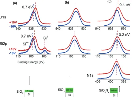
Figure 1. Si 2p, O 1s, and N 1s regions under+10 and-10 V dc bias for SiO2samples, one of them containing∼6-nm and the other ∼300-nm oxide layer together with a∼300-nm composite siliconoxynitride sample.
samples with intermediate compositions was accepted as evidence for the presence of SiO2and TiO2as separate phases.33,42The presence of SisOsTi, confirming the presence of a single phase containing both Si and Ti was also claimed by FT-IR spectra of SiO2, TiO2, and mixtures. However, the FT-IR data do not provide enough evidence for the formation of a single phase or separate phases in these samples,41and none of the previous approaches can provide indisputable evidence about the presence or absence of different domains or phases. As we will demonstrate below, our method, by controlling the charging capacity of different components in composite films, provides a clear experimental tool for differentiation of domains that are chemically/electrically distinct.
EXPERIMENTAL SECTION
A Kratos ES300 electron spectrometer with Mg KR X-rays (nonmonochromatic) was used for XPS measurements. In the standard geometry, the sample accepts X-rays at 45°and emitted photoelectrons at 90°with respect to its surface plane are analyzed. Samples were electrically connected to the sample holder, which was grounded or externally biased with a dc power supply.
Resolution of our spectrometer is slightly better than 0.80 eV as measured in the Ag 3d peaks. Since we extract binding energy differences by fitting the entire set of peaks, we estimate our error in measuring the binding energy differences to be better than 0.1 eV. FT-IR spectra of the samples were obtained using a Bruker Tensor FTIR system operating in the mid-infrared region, i.e., 400-4000 cm-1.
Silicon nitride films were deposited on p-type silicon wafer of orientation (100) using disilane (2% in nitrogen) and ammonia as reactant gases in a PECVD reactor (PlasmaLab 8510C) at a sample temperature of 350°C and a process pressure of 1000 mTorr under an applied rf power of 10 W. Afterward, the samples were annealed in air at 1100°C for 10 min. The composite SiOx+ TiOysample
was obtained by depositing a thin layer of titanium onto a silicon substrate.
RESULTS AND DISCUSSION
As we have shown in our previous publications, the silicon oxide dielectric layer develops an overall positive charge which is reflected in the Si 2p, O 1s, and SiKLLAuger peaks. This is best demonstrated in thin (<10 nm) oxide layers on a silicon wafer when both the silicon and silicon oxide Si 2p peaks are observable by XPS, and the measured binding energy difference between them exceeds the true chemical shift of 3.2 eV.1We have also shown that the measured difference can be controlled by an external bias as reproduced again in Figure 1a for a sample containing∼6-nm thermal oxide layer.22,24As can be gathered from the figure, the Si0peak is not influenced by the bias but both the Si4+and the O 1s peaks are affected by as much as 0.7 eV after altering the polarity of the bias. Under positive bias, more of the neutralizing low-energy electrons are attracted to the sample hence reducing the extent of the positive charge. For a thicker oxide sample, only the peaks of the oxide layer are accessible. As shown in Figure 1b, both the Si 2p and the O 1s peaks are broadened (due probably to enhanced charging), but again, both peaks display similar shifts under external bias as opposed to the case of the oxynitride sample of a comparable thickness as shown in (42) Brunet-Bruneau, A.; Fisson, S.; Gallas, B.; Vuye, G.; Rivory, J. Proc.
SPIE-Int. Soc. Opt. Eng.1999, 3738, 188-196.
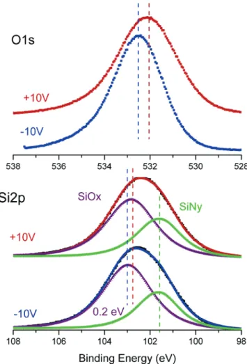
Figure 2. Si 2p and O 1s regions of XPS spectrum of composite siliconoxynitride sample upon annealing at 1100°C with+10 and -10 V external dc biases applied to the sample rod.
Figure 3. Part of the FT-IR spectra of the composite siliconoxyni-tride sample before and after annealing at 1100°C.
Figure 1c. Oxygen is present in all samples, but nitrogen is only present in the oxynitride sample and can be assigned to N3-.1In the oxynitride sample, we detect differences in the positions of both the Si 2p (0.2 eV) and the O 1s (0.4 eV) peaks, and no difference can be detected in the N 1s peak position, after changing the polarity of the bias. We take this as a spectral signature of the presence of at least two chemically different domains. One of the domains is probably pure silicon nitride, since the N 1s corresponds to that of the Si3N4. The other one cannot be assigned to pure oxide, since the shift in the Si 2p is only half of the shift in the O 1s. In order to gain more insight, we attempted to mathematically decompose the Si 2p peak into two components as shown in Figure 2: one belonging to pure nitride, and the other to the oxynitride to support our conclusion that these are the two chemically different domains (silicon nitride and silicon oxyni-tride). We should also stress that shifts observed in Figures 1 and 2 are measured only after the sample is annealed at 1100°C. The presence of different domains is also partially supported by FT-IR spectra of the silicon oxynitride film recorded before and after annealing as illustrated in Figure 3. Before annealing, the spectrum has a main absorption peaks around 870 cm-1and at 1068 cm-1, which are associated with the absorption peaks of Sis NO and SisO bonds, respectively.31After annealing, the absorp-tion peak shifts toward 840 cm-1, which is characteristic of the SisN bond.
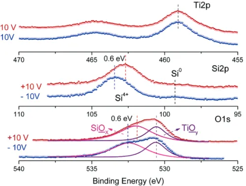
Ti 2p, Si 2p, and O 1s regions of the XPS spectra of the other composite film containing both titanium and silicon oxides on a silicon substrate, recorded when the sample is subjected to +10
and -10 V external bias, are shown in Figure 4. Whereas, no difference can be detected in Ti 2p upon reversal of the polarity of the bias, as much as 0.6 eV difference can be induced in the Si 2p peak. Accordingly, the O 1s peak can be successfully fitted to two components: one exhibiting no shift that can be assigned as titanium oxide domains, and the other, which exhibits 0.6 eV difference, to that of the silicon oxide domains. Hence, by controlling their charging capacity, we enforce domains to be separated and identified (charge contrast).
CONCLUSIONS
In this study, we demonstrate that by imposing a simple external voltage stress to the sample rod, while acquiring XPS data, we are able to control and measure the potential(s) developed as a result of charging in and on different domains. This simple charge-contrasting procedure introduces to XPS a capability to differentiate and determine the presence or absence of chemically/ electrically distinct domains in composite surface structures. ACKNOWLEDGMENT
This work was partially supported by TUBA (Turkish Academy of Sciences) and by TUBITAK (The Scientific and Technological Research Council of Turkey) through the Grant 105M094.
Received for review July 26, 2006. Accepted October 10, 2006.
AC0613683
Figure 4. Ti 2p, Si 2p, and O 1s regions of the XPS spectrum of a TiO2/SiO2composite sample recorded while applying-10 and+10 V external bias.