www.pss-rapid.com
pss
Silicon nanoparticle charge trapping
memory cell
Nazek El-Atab*, 1
, Ayse Ozcan2, 3
, Sabri Alkis2, 3
, Ali K. Okyay2, 3, 4
, and Ammar Nayfeh1
1 Institute Center for Microsystems – iMicro, Department of Electrical Engineering and Computer Science (EECS),
Masdar Institute of Science and Technology Abu Dhabi, United Arab Emirates
2 UNAM-National Nanotechnology Research Center, Bilkent University, 06800 Ankara, Turkey 3 Institute of Materials Science and Nanotechnology, Bilkent University, 06800 Ankara, Turkey 4 Department of Electrical and Electronics Engineering, Bilkent University, 06800 Ankara, Turkey
Received 3 April 2014, revised 7 May 2014, accepted 7 May 2014 Published online 12 May 2014
Keywords Si nanoparticles, ZnO, charge trapping memories, Al2O3, phonon-assisted tunneling, atomic layer deposition
* Corresponding author: e-mail [email protected]
© 2014 WILEY-VCH Verlag GmbH & Co. KGaA, Weinheim
1 Introduction Silicon nanoparticles (NPs) are con-sidered as good candidates for charge trapping and storage elements for future low voltage and high density nonvola-tile charge trapping memory devices [1–4]. In addition, it is validated recently that the use of ZnO leads through
promising low-cost memory device fabrications[5–7].
Ear-lier, we demonstrated a ZnO-based memory with 2 nm Si NPs embedded in a ZnO charge trapping layer [4]. The structure showed a large memory window at very low op-erating voltages. This was attributed to the Poole–Frenkel emission of charges at low electric fields. In this work, a memory structure with only 2 nm average size Si NPs and without ZnO charge trapping layer is investigated. Com-pared to Ref. [4], this structure enables a better understand-ing of the charge trappunderstand-ing characteristics of the 2 nm Si NPs. Also, the elimination of the ZnO layers reduces the gate stack thickness which would allow for further increas-ing the density of the memories. A diagram regardincreas-ing the fabricated memory device is given along with a
transmis-sion electron microscope (TEM) image of Si NPs and the effect of the Si NPs on the device performance is shown with electrical measurements. The emission mechanism is
determined by studying the Vt shift vs. electric field across
the tunnel oxide.
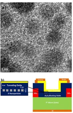
2 Fabrication Dispersed silicon nanoparticles of size 5–100 nm are first produced by applying a pulsed laser on a silicon target wafer which is submerged in de-ionized water. The femtosecond pulsed laser has a pulse duration of 200 fs, a wavelength λ = 800 nm, an average output power of 1.6 W, and a pulse repetition rate of 1 kHz which corresponds to an energy of 1.6 mJ. The Si NPs are then treated in an ultrasound bath for 200 min with an operating frequency of 40 kHz. Finally, filters with pore size of 100 nm are used to remove large parti- cles leaving a solution of Si NPs of predominately 2 nm
in size (ranging from 1–5.5 nm)[8]. A TEM image of
the synthesized Si NPs is depicted in Fig. 1a. The image A charge trapping memory with 2 nm silicon nanoparticles
(Si NPs) is demonstrated. A zinc oxide (ZnO) active layer is deposited by atomic layer deposition (ALD), preceded by Al2O3 which acts as the gate, blocking and tunneling oxide.
Spin coating technique is used to deposit Si NPs across the sample between Al2O3 steps. The Si nanoparticle memory
exhibits a threshold voltage (Vt) shift of 2.9 V at a negative
programming voltage of –10 V indicating that holes are emit-ted from channel to charge trapping layer. The negligible measured Vt shift without the nanoparticles and the good
tention of charges (>10 years) with Si NPs confirm that the Si NPs act as deep energy states within the bandgap of the Al2O3
layer. In order to determine the mechanism for hole emission, we study the effect of the electric field across the tunnel oxide on the magnitude and trend of the Vt shift. The Vt shift is only
achieved at electric fields above 1 MV/cm. This high field in-dicates that tunneling is the main mechanism. More specifi-cally, phonon-assisted tunneling (PAT) dominates at electric fields between 1.2 MV/cm < E < 2.1 MV/cm, while Fowler– Nordheim tunneling leads at higher fields (E > 2.1 MV/cm).
Figure 1 (a) TEM image of the synthesized silicon nanoparticles. (b) Cross-sectional illustration of the fabricated charge trapping memory with 2 nm Si nanoparticles.
shows that ultra-small and dispersed Si NPs are fabri- cated.
The bottom-gate memory cells are fabricated on a highly doped (10–18 mΩ cm) p-type (111) Si wafer. First,
a 360 nm thick SiO2 layer for device isolation is deposited
using plasma enhanced chemical vapor deposition
(PECVD). Then, the SiO2 layer is patterned by optical
lithography and etched using the buffered oxide etch (BOE) for 7 min. Using a Cambridge Nanotech Savannah 100 atomic layer deposition (ALD) system, a 15 nm thick
Al2O3 blocking oxide is deposited at 250 °C.
Next, Si NPs are delivered by spin coating the NPs solution at a speed of 700 rpm and an acceleration of
250 rpm/sec for 10 sec. A 4 nm thick Al2O3 tunneling
ox-ide and an 11 nm thick ZnO channel are then deposited by ALD. After patterning the ZnO channel by optical
lithog-raphy, it is etched in a solution of 98:2 H2O:H2SO4. The
source and drain contacts are created by thermally evapo-rating 100 nm Al followed by lift off. Lastly, rapid thermal
annealing (RTA) in forming gas (H2:N2 5:95) at 400 ºC
for 10 min is performed on the devices. The fabricated memory cell structure is depicted in Fig. 1b.
3 Experimental characterization The charging
effect of the Si NPs is analyzed by studying the Idrain–Vgate
curves of the programmed and erased states of memory devices with and without Si NPs. Using the Agilent-
Figure 2 (a) Id–Vg of the memory showing Vt shift with and
without Si nanoparticles. The memory is programmed by apply-ing Vg = –10 V for 5 sec. (b) Threshold voltage shift vs.
pro-gramming voltage with and without Si NPs. (c) Vt shift vs. time
extrapolated to 10 years with 2 nm Si nanoparticles.
Signatone B1505A device analyzer, the memory cells are programmed/erased by applying a gate voltage of –10 V/10 V for 5 sec. Then, the gate voltage is swept from
0 V up to 20 V with a drain voltage Vd of 10 V in order to
read the state of the cell. In fact, applying a negative gate voltage would program the memory and a positive gate voltage would erase it. This confirms that holes are emitted
into the Si NPs. The obtained Vt shift with Si NPs is 2.9 V
while it is negligible without NPs as shown in Fig. 2a. This
proves that Al2O3 of thickness up to 19 nm has a negligible
trapping density which makes this oxide an excellent can-didate for tunnel and blocking oxides. Assuming the shift in the threshold voltage is mainly due to the trapped charges in the trapping layer, the charge trap states density can be calculated by adopting Eq. (1) [9],
t Δ t , 2 C V Q q ◊ = ◊ (1)
where Ct is the capacitance of the charge trapping layer per
unit area, ΔVt is the Vt shift, and q is the elementary charge.
For a 2.9 V Vt shift, the charge trap states density is
rough-ly 7 × 1012 cm–2.
In addition, the erased state (also fresh state) of the memory with Si NPs is shifted to the right with respect to the eased state of the memory without NPs as shown in Fig. 2a. The right shift of the threshold voltage indicates that the 2 nm laser synthesized Si NPs are initially nega-tively charged. The value of the initial negative charge on the Si NPs can be calculated using Eq. (1) which results in
a charge density of 7 × 1012 cm–2. During the programming
operation, at a negative applied gate voltage, the Si NPs initial negative charge increases the electric filed across the tunnel oxide, thus enhancing the effect of hole injec- tion.
Additionally, the mean and standard deviation of the
measured Vt shifts at different programming voltages with
and without nanoparticles are shown in Fig. 2b. With Si
NPs, the Vt shift at a programming voltage of –8 V is
around 1.4 V. Figure 2b confirms that Si NPs act as charge trapping centers with high trapping density. Also, the
stand-ard deviation of the measured Vt shifts with Si NPs are
higher owing to the non-uniformity of the distribution of the Si NPs by spin coating in addition to the different number and size of the Si NPs creating the charge trapping layer of each memory cell.
Moreover, the retention characteristic of the Si NPs is
analyzed by plotting the Vt shift vs. time as shown in
Fig. 2c. The curve is extrapolated to 10 years where the
memory cell exhibits a noticeable Vt shift of 1.25 V, which
means a loss of 57% of the initial charge in 10 years. The retention of the memory cell is due to the good confine-ment of holes in the nanoparticles.
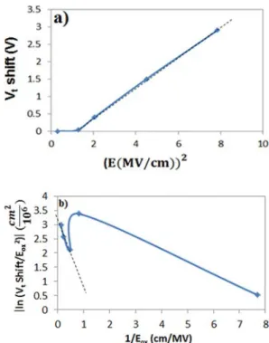
4 Analysis In order to determine the mechanism of
holes emission, Vt shift versus the square of the electric
field across the tunnel oxide is plotted in Fig. 3a. The elec-tric field is calculated using Synopsys Sentaurus Physics based TCAD simulations. The details of the TCAD model can be found in Refs. [10, 11]. In the simulations, size quantization effects are included by using the density gra-dient model. Also, the Lucent mobility model is used and
high-field saturation effects are accounted for. The Vt is
ex-tracted using the maximum transconductance method. The
linear relation depicted in Fig. 3a between Vt shift and the
square of the electric field confirms that phonon-assisted tunneling is the main mechanism for hole emission from the channel to the Si NPs charge trapping layer at electric fields higher than 1.2 MV/cm.
The emission rate in PAT increases exponentially with the square of the electric field intensity according to Eq. (2) [12, 13]: 2 2 c ( ) e , (0) E E e E e = (2)
Figure 3 (a) Vt shift vs. square of the electric field across the
tunnel oxide showing a linear dependence indicating phonon-assisted tunneling for emission. (b) The natural logarithm of the Vt shift over the square of the electric field is plotted vs. the
re-ciprocal of the electric field. The linear trend indicates that Fow-ler–Nordheim (F–N) is the dominant emission mechanism at an oxide electric field of 2.1 MV/cm.
where e(E) and e(0) are the thermal ionization probabilities
with and without electric field E, respectively, and Ec is the
characteristic field intensity. PAT is an inelastic tunneling mechanism where the holes in the channel gain enough en-ergy from phonons and tunnel through the tunnel oxide to the Si NPs. Another possible mechanism in PAT is that holes in the channel tunnel to a trap within the tunnel oxide, lose some energy by emitting a phonon, and tunnel again to the charge trapping layer. However, since the memory
without NPs showed negligible Vt shift, then the traps in
the Al2O3 are expected to be near the interface between
Al2O3 and the ZnO channel so that they do not trap charges
with a long retention time.
In addition, the linear trend shown in Fig. 3b, where
the natural logarithm of the Vt shift over the square of the
electric field across the tunnel oxide is plotted versus the inverse of the field, shows that at electric fields larger than 2.1 MV/cm, F–N tunneling is valid. However, since F–N tunneling has a stronger dependence than PAT on the elec-tric field, then the dominant mechanism at higher fields (E > 2.1 MV/cm) is F–N tunneling. F–N tunneling is con-sidered the tunneling mechanism which requires the high-est electric field across the tunel oxide to be applicable. Therefore, a triangular energy barrier is formed due to the high electric field, and holes are injected by tunneling into the valence band of the tunnel oxide through the formed triangular barrier and then are swept by the electric field
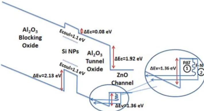
Figure 4 Energy band diagram of the Si NPs charge trapping memory at a negative applied bias. (1) Holes gain a thermal ener-gy and tunnel through the tunnel oxide through phonon-assisted tunneling (PAT), (2) holes tunnel through a triangular energy bar-rier by Fowler–Nordheim (F–N).
into the Si NPs. The emission rate of charges in F–N tun-neling follows Eq. (3) [14]:
2 ox 2 1 ox e , C E J=C E (3)
where J is the F–N tunneling current, Eox is the electric
field across the tunnel oxide, and C1 and C2 are constants
in terms of the effective mass and barrier height. Further-more, the negatively charged Si NPs enhance the electric field across the tunnel oxide allowing for PAT and F–N mechanisms to be applicable at lower electric fields.
Using the material properties of ZnO, Al2O3 [7, 15,
16], and 2 nm Si nanoparticles[17–19], the energy band
diagram of the memory cell with Si NPs is constructed and shown in Fig. 4. The changes in the electronic struc-ture of the Si NPs due to quantum confinement in 0-D [17] and to the increased charging energy are taken into account when constructing the energy band diagram. The Coulomb charging energy which represents the energy needed to add a single charge to the nanoparticle is given by Eq. (4), 2 , q E C = (4)
where q is the Coulomb charge and C is the capacitance of the nanoparticle given by 4πεR, where ε is the dielectric constant and R is the radius of the spherical nanoparticle.
The Coulomb charging energy of Si NPs of size 2 nm is calculated to be 1.1 eV and is shown in the energy band diagram plot. At 2 nm size scale, the “effective mass” for holes and electrons is similar, thus the increase in energy gap of the Si NPs from bulk silicon is partitioned and add-ed equally to both the valence band and conduction band [20]. Figure 4 shows that the conduction band offset
be-tween channel and tunnel oxide (ΔEc = 1.92 eV) is larger
than the valence band offset (ΔEv = 1.36 eV), which makes
the tunneling probability of holes through the tunnel oxide much higher than electrons probability of tunneling.
Additionally, because the electron affinity is reduced
as the size of the NPs shrinks[19], the conduction band
minimum of the Si NPs is above that of the adjacent Al2O3
by 0.08 eV which might prevent electrons storage, but the valence band minimum of the Si NPs is beyond that of the
adjacent Al2O3 by 2.13 eV so a quantum well is formed
where holes can be confined in. This analysis supports the observed hole trapping in the Si NPs. Figure 4 illus-trates the PAT and F–N mechanisms for hole emission from the channel to Si NPs. In the earlier work with the ZnO layer, lower operating voltage was achieved since the mechanism driving the emission was Poole–Frenkel effect (PFE). The electric field needed is less than 1 MV/cm since the ZnO layer adds available trap states to assist the emission [4].
5 Conclusion A Si nanoparticle charge trapping
memory is demonstrated. A 2.9 V Vt shift at –10 V
pro-gramming voltage is achieved with the Si NPs. This confirms that the laser-synthesized Si NPs behave as trapping centers with high trapping density. The domi- nant mechanism for hole emission is found to be PAT when 1.2 MV/cm < E < 2.1 MV/cm, and F–N when
E > 2.1 MV/cm. The negatively charged nature of the Si
NPs helps in increasing the electric filed across the tunnel oxide during the program function, allowing for an en-hanced hole injection through PAT and F–N. The results highlight the importance of the emission mechanism on the magnitude of the voltage needed to achieve the memory ef-fect. The good retention time of the memory allows for fur-ther scaling of the tunnel oxide without compromising the
Vt shift or retention. Finally, these results show that Si NPs
are a good candidate for charge trapping layers in future low-cost nonvolatile memory devices.
Acknowledgements We gratefully acknowledge financial
support for this work provided by the Advanced Technology Investment Company (ATIC) Grant 12RAZB7. This work was supported in part by TUBITAK Grants 109E044, 112M004, 112E052 and 113M815.
Supporting Information Available online at www.pss-rapid.com.
References
[1] N. Nedev, D. Nesheva, E. Manolov, R. Brüggemann, S. Meier, Z. Levi, and R. Zlatev, J. Phys. Conf. Ser. 113, 012034–012039 (2008).
[2] L. Wang, M. Ji, S. Zhu, H. Tu, and J. Du, J. Phys. Conf. Ser.
152, 012028–012033 (2009).
[3] H. H. I. Hanafi, S. Tiwari, and I. Khan, IEEE Trans. Elec-tron Devices 43, 1553–1558 (1996).
[4] N. El-Atab, A. Ozcan, S. Alkis, A. K. Okyay, and A. Nayfeh, Appl. Phys. Lett. 104, 013112–013115 (2014). [5] N. El-Atab, S. Alqatari, F. B. Oruc, T. Souier, M. Chiesa,
A. K. Okyay, and A. Nayfeh, AIP Adv. 3, 102119–102126 (2013).
[6] F. B. Oruc, F. Cimen, A. Rizk, M. Ghaffari, A. Nayfeh, and A. K. Okyay, IEEE Electron Device Lett. 33, 1714–1716 (2012).
[7] N. El-Atab, A. Rizk, A. K. Okyay, and A. Nayfeh, AIP Adv. 3, 112116 (2013).
[8] S. Alkis, A. K. Okyay, and B. Ortac, J. Phys. Chem. 116, 3432–3436 (2012).
[9] C. W. Liu, C. L. Cheng, S. W. Huang, J. T. Jeng, S. H. Shiau, and B. T. Dai, Appl. Phys. Lett. 91, 042107 (2007). [10] A. Alnuaimi, A. Nayfeh, and V. Koldyaev, J. Appl. Phys.
113, 044513–044519 (2013).
[11] J. Bu and M. H. White, Solid-State Electron. 45, 113–120 (2001).
[12] S. D. Ganichev, W. Prettl, and P. G. Huggard, Phys. Rev.
71, 3882–3885 (1993).
[13] S. D. Ganichev, I. N. Yassievich, W. Prettl, J. Diener, B. K. Meyer, and K. W. Benz, Phys. Rev. Lett. 75, 1590–1594 (1995).
[14] S. M. Sze, Nonvolatile Memory Devices, in: Physics of Semiconductor Devices, 3rd ed. (Wiley, 2007, New Jersey), chap. 6, s. 7, p. 353.
[15] M. L. Huang, Y. C. Chang, C. H. Chang, T. D. Lin, J. Kwo, T. B. Wu, and M. Hong, Appl. Phys. Lett. 89, 012903– 012906 (2006).
[16] G. D. Wilk, R. M. Wallace, and J. M. Anthony, J. Appl. Phys. 89, 5243 (2001).
[17] J. P. Proot, C. Delerue, and G. Allan,Appl. Phys. Lett. 61, 1948–1950 (1992).
[18] C. Delerue and G. Allan, Appl. Phys. Lett. 88, 173117–
173120 (2006).
[19] D. V. Melnikov and J. R. Chelikowsky, Phys. Rev. B 69, 113305–113309 (2004).
[20] O. M. Nayfeh, Ph.D. dissertation, EECS, MIT, Cambridge, MA (2009).