PLASMONICALLY ENHANCED HOT
ELECTRON BASED OPTOELECTRONIC
DEVICES
a dissertation submitted to
the graduate school of engineering and science
of bilkent university
in partial fulfillment of the requirements for
the degree of
doctor of philosophy
in
electrical and electronics engineering
By
Fatih Bilge Atar
June, 2015
PLASMONICALLY ENHANCED HOT ELECTRON BASED OPTOELECTRONIC DEVICES
By Fatih Bilge Atar June, 2015
We certify that we have read this thesis and that in our opinion it is fully adequate, in scope and in quality, as a dissertation for the degree of Doctor of Philosophy.
Assist. Prof. Dr. Ali Kemal Okyay(Advisor)
Prof. Dr. Mehmet Bayındır
Assoc. Prof. Dr. Hilmi Volkan Demir
Assoc. Prof. Dr. Mustafa Alevli
Assist. Prof. Dr. ˙Ibrahim Yılmaz
Approved for the Graduate School of Engineering and Science:
Prof. Dr. Levent Onural Director of the Graduate School
ABSTRACT
PLASMONICALLY ENHANCED HOT ELECTRON
BASED OPTOELECTRONIC DEVICES
Fatih Bilge Atar
Ph.D. in Electrical and Electronics Engineering Advisor: Assist. Prof. Dr. Ali Kemal Okyay
June, 2015
Hot electron based optoelectronic devices have been regarded as cost-effective candidates to their conventional counterparts. The efficiency of conventional optoelectronic devices that rely on semiconductor photo-absorbers are mainly limited by the energy bandgap of the semiconductor. On the other hand, hot electron devices can overcome this limitation via the “internal photoemission” mechanism. Absorbed photons give their energy to free electrons of the metal and these high energy (“hot”) electrons can be used to generate photocurrent in proper device configurations. High optical reflection from metals has remained as the main drawback of this photocurrent generation scheme but this problem has recently been addressed by the use of surface plasmons. Optical energy can be tightly confined to a metal layer or metal nanostructures in the form of surface plasmons, and the decay of surface plasmons in metals generates hot electrons.
In this work, we study mechanisms of surface plasmon excitation, surface plas-mon decay, hot electron generation and hot electron photoemission for photocur-rent generation. We demonstrate novel device architectures and plasmon excita-tion structures. We demonstrate the use of such layers for plasmon enhanced hot electron based photodetectors and photovoltaic devices. A metal-semiconductor Schottky junction diode structure is used as hot electron photodetector. A dou-ble metal-insulator-metal (MIM) architecture is proposed as a hot electron pho-tovoltaic device. Full wave electromagnetic simulations of these device structures are conducted to provide insight into the surface plasmon assisted hot electron generation process and give future directions in this field.
Keywords: Hot electron, surface plasmon, optoelectronics, internal photoemis-sion, photodetectors, photovoltaics.
¨
OZET
PLAZMON DESTEKL˙I SICAK ELEKTRON TABANLI
OPTOELEKTRON˙IK AYGITLAR
Fatih Bilge Atar
Elektrik ve Elektronik M¨uhendisli˘gi, Doktora Tez Danı¸smanı: Assist. Prof. Dr. Ali Kemal Okyay
Haziran, 2015
Sıcak elektron tabanlı optoelektronik aygıtlar geleneksel aygıtların d¨u¸s¨uk maliyetli alternatifleri olarak ilgi g¨orm¨u¸slerdir. Bilinen optoelektronik aygıtların verimi ¸co˘gunlukla ı¸sık so˘gurucu olarak kullanılan yarı-iletkenin enerji bant aralı˘gıyla limitlidir. ¨Ote yandan sıcak elektron aygıtları i¸c fotoemisyon mekaniz-ması ile bu limiti a¸sabilmektedirler. Bir metal i¸cerisinde emilen fotonlar sahip oldukları enerjiyi metalin serbest elektronlarına vererek elektronları daha y¨uksek enerji seviyelerine ¸cıkartırlar. Y¨uksek enerjiye sahip bu sıcak elektronlar uygun aygıt yapılarında fotoakım ¨uretmek i¸cin kullanılabilirler. Bu y¨ontemin ¨on¨undeki en b¨uy¨uk engel, metal y¨uzeylerin yansıtıcı ¨ozelli˘ge sahip olmalarıdır. Y¨uzey plaz-monlarının kullanılması bu engelin ¨onemli ¨ol¸c¨ude a¸sılmasını sa˘glamı¸stır. I¸sık en-erjisi, y¨uzey plazmonları halinde metal katmanlara veya metal nanopar¸cacıklara hapsedilerek metal i¸cerisindeki ı¸sık emiliminin artması sa˘glanır. Bu sayede metal i¸cerisindeki sıcak elektron olu¸sma hızı da artırılır.
Bu ¸calı¸smada y¨uzey plazmonlarının tetiklenme ve s¨on¨umlenme mekanizmaları, y¨uzey plazmonlarının s¨on¨umlenmesi ile sıcak elektron olu¸sumu ve sıcak elektron-ların fotoemisyonuyla fotoakım olu¸sumu incelenmi¸stir. ¨Ozg¨un aygıt mimarileri ve plazmon tetikleme yapıları ¨uzerine ¸calı¸sılmı¸s ve bu yapılarla plazmon destekli sıcak elektron tabanlı fotodedekt¨orler ve fotovoltaik aygıtlar g¨osterilmi¸stir. Metal-yarıiletken Schottky eklem diyot yapısı sıcak elektron tabanlı fotodedekt¨or olarak kullanılmı¸stır. C¸ ift katlı metal-yalıtkan-metal (MYM) mimarisi sıcak elektron tabanlı fotovoltaik aygıt olarak ¨onerilmi¸stir. Bu aygıtların tam dalga elektromanyetik simulasyonları yapılarak plazmon destekli sıcak elektron olu¸sma mekanizması a¸cıklanmı¸s ve bu alanda yapılacak ¸calı¸smalar i¸cin yol g¨osterici bul-gular sunulmu¸stur.
Anahtar s¨ozc¨ukler : Sıcak elektron, y¨uzey plazmonları, optoelektronik, i¸c fo-toemisyon, fotodedekt¨or, fotovoltaik.
Acknowledgement
I would like to start by expressing my deepest gratitude to Prof. Ali Kemal Okyay for his guidance and patience. He was an excellent supervisor and I am happy to be a member of his research team. I have learned a lot from him and I will always be grateful for everything he has done for me. Along with Prof. Okyay, I thank all Okyay Team members for the great time we have shared.
I would like to thank Prof. Mehmet Bayındır, Prof. Hilmi Volkan Demir, Prof. Mustafa Alevli and Prof. ˙Ibrahim Yılmaz for being members of my thesis committee and making this dissertation better with their valuable opinion.
I would like to acknowledge T ¨UB˙ITAK (The Scientific and Technological Re-search Council of Turkey) for providing me a Ph.D. scholarship and funding our research. I appreciate their generous support that enabled these studies. I have to thank The Department of Electrical and Electronics Engineering of Bilkent University and UNAM (National Nanotechnology Research Center) for providing the facilities and equipment for our research.
My 10-year-long stay in Bilkent has been an invaluable experience. I would like to thank Prof. ˙Ihsan Do˘gramacı, the founder of Bilkent University, and all Bilkent community for every joyful moment I spent in Bilkent. I also would like to thank all faculty members for the great education and inspiration they provided. Finally, I would like to express my gratitude to my family. Any success I may have achieved would not have been possible without their love and support. Along with them, I have to thank many great friends who have been another family to me and contributed to this dissertation in many different ways. Undoubtedly, this dissertation is dedicated to my family.
Contents
1 Introduction 1
2 Hot Electron Based Photodetection 9
2.1 Internal Photoemission . . . 9
2.2 Metal-Semiconductor (MS) Schottky Junction . . . 11
2.3 Metal-Insulator-Semiconductor (MIS) Junction . . . 13
2.4 MIS Solar Cells . . . 14
2.5 Conclusion . . . 18
3 Surface Plasmon Assisted Hot Electron Generation 19 3.1 Introduction . . . 19
3.2 Localized Surface Plasmon Resonances . . . 21
3.3 Plasmon Assisted Hot Electron Generation . . . 24
4 Plasmonic nanoantennas for sub-bandgap photodetection 29 4.1 Introduction . . . 29
4.2 Device Architecture . . . 30
4.3 Chemical Synthesis of Au Nanoparticles . . . 31
4.4 Random Au Nanoparticles with Thermal Annealing Method . . . 32
4.5 Device Fabrication . . . 33
4.6 Optoelectronic Characterization . . . 36
4.7 FDTD Simulations . . . 41
4.8 Conclusion . . . 46
5 Double MIM Photovoltaic Device 47 5.1 Introduction . . . 47
CONTENTS vii
5.2 Device Design . . . 49
5.3 Tunneling Through the Insulator . . . 51
5.4 FDTD Simulations . . . 52
5.5 Fabrication of Double MIM Structures . . . 54
5.6 Optoelectronic Characterization . . . 55
5.7 Modifications to the Double MIM Photovoltaic Device . . . 57
5.7.1 Surface Roughness . . . 57
5.7.2 Au Core-SiO2 Shell Nanoparticles . . . 58
5.7.3 Au Nanorods . . . 59
5.8 Conclusion & Future Directions . . . 61
6 Absorption Engineering in Double MIM Hot Electron Based Photovoltaic Device 65 6.1 Introduction . . . 65 6.2 Simulation Setup . . . 66 6.3 Simulation Results . . . 70 6.3.1 Au Top Metal . . . 70 6.3.2 Cr Top Metal . . . 74 6.3.3 Al Top Metal . . . 78 6.3.4 Ag Top Metal . . . 81
6.4 Surface Plasmon Modes in Double MIM Structure . . . 84
6.5 Conclusion . . . 87
List of Figures
1.1 Schematic view of a hot electron based photovoltaic device archi-tecture. Au nanoparticles are used to excite LSPR and TiO2 is
used to collect the generated hot electrons. . . 2 1.2 Comparison of two photographs taken with visible and SWIR
cam-eras. The effect of fog is significantly smaller in the image taken with the SWIR camera due to the reduced scattering of light at longer wavelengths. Copyright 2011 Society of Photo Optical In-strumentation Engineers. . . 3 1.3 (a) Energy band diagram of n-type Si showing the conduction and
valence bands. Absorption of an incident photon excites an elec-tron from the valence band to the conduction band, leaving a hole in the valence band (band-to-band absorption). Only photons with energies (hν) greater than the energy bandgap (Eg) of Si are
ab-sorbed (hν > Eg) and can create electron-hole pairs. (b) Energy
band diagram of ideal Au/n-Si Schottky junction where the work function of the metal is aligned with the Fermi level of the semi-conductor. Absorption of an incident photon excites an electron of the metal to higher energy levels and this highly energetic electron can be collected to the semiconductor over the Schottky barrier. Ideally the energy of the photon (hν) must be greater than the Schottky barrier height (ϕ), which is usually much smaller than the energy bandgap (Eg) of Si. In practice, even the photons with
energies smaller than the Schottky barrier height can contribute to the photocurrent. . . 4
LIST OF FIGURES ix
2.1 Energy band diagram of an Au/n-Si Schottky junction. Photons incident on the metal can excite the electrons of the metal to higher energy levels (hot electron generation) and these hot electrons can be emitted into the semiconductor to generate photocurrent (in-ternal photoemission). . . 10 2.2 Energy band diagrams of Au/n-Si Schottky junctions without the
work function pinning (a) and with work function pinning (b). The height of the Schottky barrier is directly affected by the pinning of the work function to another level. The shape of the Schottky bar-rier and other electrical properties are also affected by this change in the work function. . . 13 2.3 The energy band diagram of a metal-insulator-semiconductor
(MIS) junction (a) at flat-band condition and (b) under reverse bias. In the direct tunneling process (green arrows) the tunneling probability depends on the thickness and the height of the poten-tial barrier, and it is relatively independent of the bias voltage. For the electrons with sufficiently high energies, Fowler-Nordheim tunneling is observed (red arrow). The effective insulator thickness is reduced due to the bending of the energy bands with the high electric field. The tunneling probability depends on the electron energy and the bias voltage. . . 14 2.4 Energy band diagrams of two Schottky junctions with (a) highly
doped and (b) lowly doped semiconductors. Band bending is greater for the highly doped semiconductor (a) compared to the lowly doped semiconductor (b) due to the position of the Fermi level. The triangular shape of the barrier gets thinner as the band bending increases, resulting in an increase in the tunneling proba-bility of the hot electrons at these energy levels (Fowler-Nordheim tunneling). . . 15
LIST OF FIGURES x
2.5 Dark current mechanisms in a Schottky junction are shown on the energy band diagram of a forward biased metal-insulator-semiconductor (MIS) solar cell. The thermionic emission dark cur-rent, Jth, recombination-generation current, Jrg, injection-diffusion
current, Jd, and surface state current, Js, are depicted on the
en-ergy band diagram. The thermionic emission dark current has been reported as the dominating dark current component for most practical cases. . . 16 3.1 Propagating surface plasmon polaritons (SPP) and localized
sur-face plasmon resonances (LSPR) at metal dielectric intersur-faces. SPPs can be excited by using a prism or with corrugations on the surface, and they propagate along the metal-dielectric inter-face. LSPRs are non-propagating and can be excited on metallic nanoparticles or metallic gratings even under direct illumination. 20 3.2 Possible momentum values of hot electrons form a sphere in the
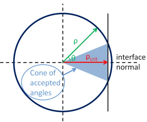
momentum space. The momentum of a hot electron should be such that its component normal to the metal-semiconductor interface should be larger than a critical value, ρcrit, which is defined by the
Schottky barrier height. This condition defines a cone of angles in the momentum space for which the hot electrons will be allowed to be emitted from the metal to the semiconductor. . . 26 3.3 (i) Incident light excites surface plasmons on Au nanoparticles.
(ii) Surface plasmons decay by giving their energy to the elec-trons of the metal, generating hot elecelec-trons. (iii) Hot elecelec-trons are injected from the metal to the semiconductor. Hot electron gener-ation and injection processes are completed within 50 fs. (iv) An electron must be replenished to the metal instead of the injected one so that the hot electron generation and injection from the metal nanoparticle can continue. The fastest reported timescales of charge regeneration process are in the order of 20 ns. . . 27
LIST OF FIGURES xi
4.1 (a) The schematic view of the hot electron based near infrared pho-todetector structure. n-type Si is used as substrate. Au nanopar-ticles on Si surface excite LSPR and generate hot electrons. An Aluminum-doped Zinc Oxide (AZO) layer forms the top contact. (b) Configuration for the optoelectronic characterization. Voltage across a resistor in series with the photodetector is used to measure the photocurrent. Biasing polarity of the device is shown on the figure. . . 31 4.2 Absorption spectrum of the Au nanoparticles synthesized by the
modified Turkevich method. The absorption spectrum is mea-sured with the Au nanoparticles in de-ionized water solution. Au nanoparticles exhibit absorption resonance at around 530 nm wave-length. Copyright 2013 Optical Society of America . . . 32 4.3 (a) SEM image of chemically synthesized Au nanoparticles coated
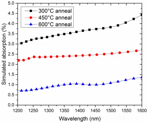
on quartz substrate. Dense and uniform nanoparticle distribu-tion could be achieved on quartz substrates. (b) SEM image of Au nanoislands formed with rapid thermal annealing of a thin Au layer on Si substrate. Instead of identical nanoparticles, elongated nanoislands with random shapes are obtained. The size distribu-tion of the nanoislands is much broader than that obtained with chemical synthesis. . . 33 4.4 SEM images of the samples annealed at 300◦C, 450◦C, and 600◦C.
The Au layer forms into a semi-continuous Au film when the an-nealing temperature is 300◦C. Increasing the annealing tempera-ture results in the separation of connected Au nanoislands to form smaller nanoislands or nanoparticles. . . 34 4.5 Particle size distribution histograms of SEM images in Fig. 4.4.
The histograms belong to samples annealed at 300◦C, 450◦C and 600◦C in order from left to right. The average nanoparticle sizes extracted from SEM images are 179 nm, 155 nm and 112 nm for samples annealed at 300◦C, 450◦C and 600◦C, respectively. The number of smaller particles is greater for the samples annealed at higher temperatures. . . 34
LIST OF FIGURES xii
4.6 Devices with different Au nanoparticle size and distribution are obtained by rapid thermal annealing of the samples at different temperatures: 300◦C, 450◦C and 600◦C. “AZO Reference” only has an AZO layer coated on Si substrate without Au nanoislands and “Au Reference” only has a flat Au layer on Si substrate without the AZO layer. . . 35 4.7 Schematic drawing of the photoresponsivity measurement setup.
A super continuum laser light is monochromated with an acousto-optic transmission filter (AOTF) and used as a monochromated light source. Laser beam is aligned with mirrors and focused on the device with an objective lens. Two beam splitters in the beam path are used to simultaneously illuminate the device with laser light and infrared LED light, and also to image the device surface with an IR camera for probing. The green arrows in the image show the path of the laser beam and the red arrows show the path of the IR illuminating beam that is imaged by the IR camera. . . 37 4.8 A photograph of the photoresponsivity measurement setup. The
acousto-optic transmission filter (AOTF), the custom designed op-tic setup and the probing system are shown in the image. . . 37 4.9 Dark current-bias voltage (I-V) measurement results of the
fab-ricated photodetectors. AZO Reference exhibits low dark cur-rent and good rectification. The other samples which have Au nanoislands and Au Reference have higher dark current due to the generation-recombination centers at the interface. . . 38 4.10 Measured photoresponsivity spectra of the fabricated
photodetec-tors. The photoresponse of the AZO Reference drops sharply for λ > 1200 nm. The Au Reference can exhibit photoresponse at these wavelengths with the internal photoemission process. Due to the excitation of surface plasmons, the devices with Au nanois-lands have significantly higher photoresponse compared to the Au Reference. The device annealed at 450◦C shows the highest pho-toresponsivity for λ < 1500 nm, and the device annealed at 300◦C shows the highest photoresponsivity for λ > 1500 nm. . . 40
LIST OF FIGURES xiii
4.11 Cross-sectional view of the 3-D simulation environment used in the first set of simulations. The structure consists of a Si substrate, Au nanoparticle and AZO top contact. Periodic boundary conditions are used for the x-axis (the horizontal axis in the images) and z-axis (perpendicular to the image plane). Perfectly matched layer (PML) boundary conditions are used for the y-axis (vertical axis in the images). . . 41 4.12 Simulated absorption spectra of the identical Au nanoparticles on
Si substrate covered by AZO layer. Surface plasmon resonance re-sults in an absorption peak at the NIR wavelengths and the wave-length of the resonance red-shifts as the nanoparticle size increases. 42 4.13 Cross-sectional view of the 3-D simulation environment used in the
second set of simulations. The structure consists of a Si substrate, randomly shaped Au nanoislands and AZO top contact. Perfectly matched layer (PML) boundary conditions are used for the z-axis (a). Periodic boundary conditions are used for the x-axis and y-axis (b). . . 43 4.14 Simulated absorption spectra of the randomly shaped Au
nanois-lands on Si substrate covered by AZO layer. The random shape of the Au nanoislands was obtained by importing a unit cell from the SEM images and assuming the unit cell to be periodic in x and y directions. Overall response of randomly shaped plasmonic res-onators results in a broad-band absorptivity spectrum. The device annealed at the lowest temperature (300◦C) has the largest aver-age nanoisland size hence shows the highest absorptivity at the NIR wavelengths and the absorption increases as the wavelength increases. . . 44 4.15 Calculated photoresponsivity spectra for the samples annealed at
300◦C, 450◦C and 600◦C. Photoresponsivity spectra are calculated as the product of the absorption spectra shown in Fig. 4.14 and the Fowler function. Fowler emission coefficient and the Schottky barrier height are used to fit the calculated absorption spectra to the experimental results. . . 45
LIST OF FIGURES xiv
5.1 (a) Surface plasmon excitation on the metal-air interface by using a prism in Kretschmann arrangement. (b) Use of Kretschmann arrangement to excite surface plasmons on the metal-air interface of an MIM photovoltaic device . . . 49 5.2 (a) The schematic view of the proposed hot electron based
pho-tovoltaic device architecture. Au-HfO2-Al layers (bottom MIM)
acts as a diode. Au NP-Al2O3-Au layers excite surface plasmons
under direct illumination and localize the electromagnetic field in the Au layer. (b) SEM image of the Au nanoparticles randomly distributed on the device surface. . . 50 5.3 The energy band diagram of the MIM diode with Au-HfO2-Al
lay-ers. The photoexcited hot electrons diffuse in random directions in the Au layer. The hot electrons that reach the junction with sufficient momentum normal to the Au-HfO2 interface can travel
over the potential barrier or tunnel through it and generate pho-tocurrent (internal photoemission). . . 51 5.4 Electric field intensity profiles at λ = 590 nm obtained by FDTD
simulations (a) Planar MIM structure without Au nanoparticles. Incident light is mostly reflected back and only a very small por-tion of the electromagnetic field can penetrate into the metal layer to be absorbed by the metal (b) MIM structure with Au nanopar-ticles on top. Au nanoparnanopar-ticles excite LSPRs and trigger SPP modes at metal-insulator interfaces, which significantly enhance the electromagnetic field in the Au layer. Scattering of light by these nanoparticles also excite the dark modes in the underlying MIM structure. . . 54
LIST OF FIGURES xv
5.5 Enhancement of the absorption in the Au layer due to the exci-tation of LSPRs on Au nanoparticles and exciexci-tation of SPPs on metal-insulator interfaces. Total absorption spectra in the metal layer are calculated with FDTD simulations for the two cases: (i) MIM device with Au nanoparticles (ii) bare MIM device (without Au nanoparticles). The absorption enhancement spectrum is cal-culated as the ratio of the simulated total absorption spectra of these two cases. . . 55 5.6 Measured photoresponsivity of the MIM device before and after
the spin coating of Au nanoparticles. The inset plots the ratio of the photoresponsivity spectra of two measurements. The device with Au nanoparticles shows resonant enhancement at around 700 nm wavelength. . . 57 5.7 Top view SEM images of completed MIM devices with spin coated
Au nanoparticles. Bottom metal (Al) was thermally evaporated on Si substrate at (a) 0.7 ˚A/s deposition rate (b) 5 ˚A/s deposition rate. . . 58 5.8 Measured photoresponsivity of the MIM device before and after the
spin coating of Au nanoparticles. The inset plots the ratio of the photoresponsivity spectra of two measurements. When the surface roughness is reduced, the plasmonic resonances make a blue-shift and the center frequency of the plasmonic resonance moves to 600 nm wavelength. . . 59 5.9 Measured photoresponsivity spectrum of the device before and
af-ter the spin coating of Au core-SiO2 shell nanoparticles. No
reso-nant photocurrent enhancement is observed. Absorption enhance-ment occurs below the resonance frequency of Au nanoparticles, at UV wavelengths. . . 60 5.10 TEM image of Au nanorods we have used in this study. Due to
their elongated shape, nanorods are expected to show red-shifted plasmonic resonances compared to spherical nanoparticles. . . 61
LIST OF FIGURES xvi
5.11 Measured photoresponsivity of the device before and after the spin coating of Au nanorods. The device with nanorods shows reso-nant enhancement at around 800 nm wavelength. The plasmonic resonances are red-shifted compared to the devices with spherical nanoparticles (Fig. 5.8). . . 62 5.12 Measured photocurrent of the MIM device before and after the
spin coating of Au nanorods. The device with nanorods shows resonant enhancement at around 800 nm wavelength. There are artificial photocurrent peaks due to the emission peaks of the Xe lamp that is used as the light source. Still the enhancement of the photocurrent by the excitation of localized surface plasmons on nanorods is clearly visible. . . 63 6.1 Schematic drawing of the double MIM structure. The bottom
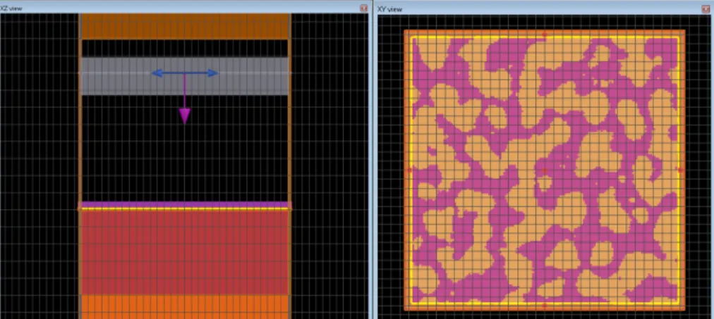
metal, the bottom insulator and the top metal layers form the bottom MIM, which will act as a diode in the actual device opera-tion. The top metal, the top insulator and the nanostructure form the top MIM, which is used to excite surface plasmon modes. . . 67 6.2 Simulation environment, depicting a unit cell of the double MIM
stack. A light source illuminates the double MIM stack from the top with direct incidence. Perfectly matched layer (PML) bound-ary conditions are used for the top and bottom boundaries (z-axis) and periodic boundary conditions are used for x and y axis. An absorption monitor covering the whole volume of the top metal is used to calculate the absorption spectrum. . . 69 6.3 Absorptivity spectrum of the Au top metal layer of the MIMIM
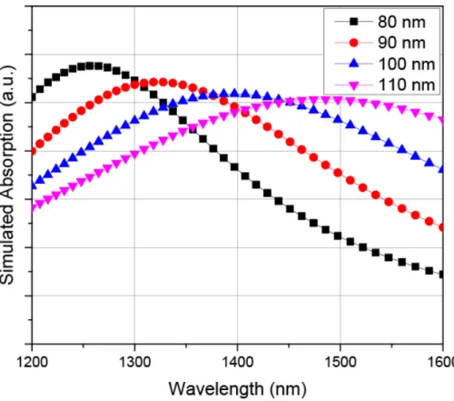
structure with 40-nm-thick top insulator and Ag nanoantenna. Simulated nanoantenna thicknesses are (a) 30 nm, (b) 50 nm, (c) 80 nm and (d) 100 nm. Different plots in each figure correspond to the reference structure and nanoantenna widths of 60 nm, 80 nm, 100 nm and 120 nm. . . 72
LIST OF FIGURES xvii
6.4 Absorptivity spectrum of the Au top metal layer of the MIMIM structure with 80-nm-thick top insulator and Ag nanoantenna. Simulated nanoantenna thicknesses are (a) 30 nm, (b) 50 nm, (c) 80 nm and (d) 100 nm. Different plots in each figure correspond to the reference structure and nanoantenna widths of 60 nm, 80 nm, 100 nm and 120 nm. . . 72 6.5 Absorptivity spectrum of the Au top metal layer of the MIMIM
structure with 40-nm-thick top insulator and Au nanoantenna. Simulated nanoantenna thicknesses are (a) 30 nm, (b) 50 nm, (c) 80 nm and (d) 100 nm. Different plots in each figure correspond to the reference structure and nanoantenna widths of 60 nm, 80 nm, 100 nm and 120 nm. . . 73 6.6 Absorptivity spectrum of the Au top metal layer of the MIMIM
structure with 80-nm-thick top insulator and Au nanoantenna. Simulated nanoantenna thicknesses are (a) 30 nm, (b) 50 nm, (c) 80 nm and (d) 100 nm. Different plots in each figure correspond to the reference structure and nanoantenna widths of 60 nm, 80 nm, 100 nm and 120 nm. . . 73 6.7 Absorptivity in the top metal (Cr) layer of Al-Al2O3-Cr-Al2O3
(MIM) device. Increasing the top insulator thickness red-shifts the absorptivity spectrum. . . 74 6.8 Absorptivity spectrum of the Cr top metal layer of the MIMIM
structure with 40-nm-thick top insulator and Ag nanoantenna. Simulated nanoantenna thicknesses are (a) 30 nm, (b) 50 nm, (c) 80 nm and (d) 100 nm. Different plots in each figure correspond to the reference structure and nanoantenna widths of 60 nm, 80 nm, 100 nm and 120 nm. . . 76 6.9 Absorptivity spectrum of the Cr top metal layer of the MIMIM
structure with 80-nm-thick top insulator and Ag nanoantenna. Simulated nanoantenna thicknesses are (a) 30 nm, (b) 50 nm, (c) 80 nm and (d) 100 nm. Different plots in each figure correspond to the reference structure and nanoantenna widths of 60 nm, 80 nm, 100 nm and 120 nm. . . 76
LIST OF FIGURES xviii
6.10 Absorptivity spectrum of the Cr top metal layer of the MIMIM structure with 40-nm-thick top insulator and Au nanoantenna. Simulated nanoantenna thicknesses are (a) 30 nm, (b) 50 nm, (c) 80 nm and (d) 100 nm. Different plots in each figure correspond to the reference structure and nanoantenna widths of 60 nm, 80 nm, 100 nm and 120 nm. . . 77 6.11 Absorptivity spectrum of the Cr top metal layer of the MIMIM
structure with 80-nm-thick top insulator and Au nanoantenna. Simulated nanoantenna thicknesses are (a) 30 nm, (b) 50 nm, (c) 80 nm and (d) 100 nm. Different plots in each figure correspond to the reference structure and nanoantenna widths of 60 nm, 80 nm, 100 nm and 120 nm. . . 77 6.12 Absorptivity spectrum of the Al top metal layer of the MIMIM
structure with 40-nm-thick top insulator and Ag nanoantenna. Simulated nanoantenna thicknesses are (a) 30 nm, (b) 50 nm, (c) 80 nm and (d) 100 nm. Different plots in each figure correspond to the reference structure and nanoantenna widths of 60 nm, 80 nm, 100 nm and 120 nm. . . 79 6.13 Absorptivity spectrum of the Al top metal layer of the MIMIM
structure with 80-nm-thick top insulator and Ag nanoantenna. Simulated nanoantenna thicknesses are (a) 30 nm, (b) 50 nm, (c) 80 nm and (d) 100 nm. Different plots in each figure correspond to the reference structure and nanoantenna widths of 60 nm, 80 nm, 100 nm and 120 nm. . . 79 6.14 Absorptivity spectrum of the Al top metal layer of the MIMIM
structure with 40-nm-thick top insulator and Au nanoantenna. Simulated nanoantenna thicknesses are (a) 30 nm, (b) 50 nm, (c) 80 nm and (d) 100 nm. Different plots in each figure correspond to the reference structure and nanoantenna widths of 60 nm, 80 nm, 100 nm and 120 nm. . . 80
LIST OF FIGURES xix
6.15 Absorptivity spectrum of the Al top metal layer of the MIMIM structure with 80-nm-thick top insulator and Au nanoantenna. Simulated nanoantenna thicknesses are (a) 30 nm, (b) 50 nm, (c) 80 nm and (d) 100 nm. Different plots in each figure correspond to the reference structure and nanoantenna widths of 60 nm, 80 nm, 100 nm and 120 nm. . . 80 6.16 Absorptivity spectrum of the Ag top metal layer of the MIMIM
structure with 40-nm-thick top insulator and Ag nanoantenna. Simulated nanoantenna thicknesses are (a) 30 nm, (b) 50 nm, (c) 80 nm and (d) 100 nm. Different plots in each figure correspond to the reference structure and nanoantenna widths of 60 nm, 80 nm, 100 nm and 120 nm. . . 82 6.17 Absorptivity spectrum of the Ag top metal layer of the MIMIM
structure with 80-nm-thick top insulator and Ag nanoantenna. Simulated nanoantenna thicknesses are (a) 30 nm, (b) 50 nm, (c) 80 nm and (d) 100 nm. Different plots in each figure correspond to the reference structure and nanoantenna widths of 60 nm, 80 nm, 100 nm and 120 nm. . . 82 6.18 Absorptivity spectrum of the Ag top metal layer of the MIMIM
structure with 40-nm-thick top insulator and Au nanoantenna. Simulated nanoantenna thicknesses are (a) 30 nm, (b) 50 nm, (c) 80 nm and (d) 100 nm. Different plots in each figure correspond to the reference structure and nanoantenna widths of 60 nm, 80 nm, 100 nm and 120 nm. . . 83 6.19 Absorptivity spectrum of the Ag top metal layer of the MIMIM
structure with 80-nm-thick top insulator and Au nanoantenna. Simulated nanoantenna thicknesses are (a) 30 nm, (b) 50 nm, (c) 80 nm and (d) 100 nm. Different plots in each figure correspond to the reference structure and nanoantenna widths of 60 nm, 80 nm, 100 nm and 120 nm. . . 83
LIST OF FIGURES xx
6.20 Bonding (a) and antibonding (b) interaction between two metal nanostructures standing next to each other on a substrate. The bonding mode can be excited with normal incidence and is called the bright mode. The antibonding mode can not be excited in this configuration and is called the dark mode. The MIM configuration allows the excitation of both the antibonding (c) and bonding (d) modes under normally incident light. . . 85 6.21 Simulated electric field profile of the double MIM structure at 550
nm wavelength for the same device configuration as Fig. 6.5. The thickness of the nanoantenna is 50 nm and the width of the nanoan-tenna is 100 nm. Electric field is mostly concentrated around the Au nanoantenna, outside the MIM structure, which indicates the strong scattering of the bright plasmon mode. . . 86 6.22 Simulated electric field profile of the double MIM structure at
840 nm wavelength for the same device configuration as Fig. 6.5. The thickness of the nanoantenna is 50 nm and the width of the nanoantenna is 100 nm. Electric field is strongly confined below the Au nanoantenna, within the MIM structure, which indicates the strongly absorptive behavior of the dark plasmon mode. . . . 87
List of Tables
6.1 The structural parameters of the simulated double MIM devices in each figure. The material of the top metal, the material of the nanoantenna and the thickness of the top insulator are given for each figure. . . 70
Chapter 1
Introduction
Hot electron based optoelectronic devices have recently appeared as intriguing candidates for photodetection, photovoltaics and photocatalytic applications. The extremely low cost that the hot electron based devices offer compared to their conventional counterparts seem to be their most prominent advantage. The recent advances in the field of plasmonics have successfully addressed some key problems related to the hot electron based device technology and enabled a myr-iad of new approaches for highly efficient hot electron based devices. This study focuses on near infrared (NIR) photodetection with hot electron based devices and photovoltaic applications of hot electron based devices with a strong emphasis on plasmonic effects in these device architectures.
Direct conversion of the energy of surface plasmons to electrical energy by the generation of hot carriers in metals has been explored as an alternative approach for a new type of solar cell. This new solar energy conversion scheme is con-sidered to have the potential to exceed the efficiencies of conventional devices and the fabrication costs are expected to be lower than single crystalline Si so-lar cells or amorphous thin film soso-lar cells [1]. Hot electron based photovoltaic device architecture as proposed by Zhao et al. is illustrated in (Fig. 1.1) as an example [2]. Localized surface plasmon resonances (LSPR) are excited on Au or Ag nanoparticles upon solar illumination. The decay of surface plasmons results
in the generation of hot carriers in the metal, which are generally collected to a wide bandgap semiconductor such as TiO2 or ZnO. The lost electrons of the
metal nanoparticles must be regenerated for the hot electron generation process to continue. The basic principles and main limitations of this solar energy con-version scheme and the recent efforts to overcome these limitations are explained in the following chapters.
Figure 1.1: Schematic view of a hot electron based photovoltaic device architec-ture. Au nanoparticles are used to excite LSPR and TiO2 is used to collect the
generated hot electrons.
Surface plasmon assisted hot electron generation has also been employed in low-cost NIR photodetectors by making use of the sub-bandgap photodetection process. Despite their high cost, conventional NIR photodetectors have found extensive use in spectroscopy and imaging for biotechnology and pharmaceutical applications [3, 4]. Use of NIR photodetectors for surveillance applications has also gathered interest due to the outstanding performance of short-wave infrared (SWIR) cameras [5]. SWIR cameras can give a better view compared to visible cameras and thermal imagers, and have the capability to operate full day-night. Fig. 1.2 shows two images taken with SWIR and visible cameras for comparison [6]. The image taken with SWIR camera is not obscured by the fog since the light at longer wavelengths encounters much less scattering in the atmosphere (Rayleigh scattering ∝ 1/λ4 ). SWIR image has a clearer view and shows more
of NIR photodetectors, reducing the fabrication cost and expanding their use have been a challenge.
Figure 1.2: Comparison of two photographs taken with visible and SWIR cam-eras. The effect of fog is significantly smaller in the image taken with the SWIR camera due to the reduced scattering of light at longer wavelengths. Copyright 2011 Society of Photo Optical Instrumentation Engineers.
For any commercial photodetector configuration, the integration of the sensor with Si CMOS read-out circuitry is essential and this integration brings extra cost for most NIR photodetectors since Si itself does not detect NIR light. Heteroepi-taxy of narrow-gap semiconductors such as Ge [7, 8] or the hybrid use of com-pound semiconductors become necessary [5]. These semiconductors have smaller bandgap energy compared to Si and they can absorb the near infrared light via band-to-band absorption process (Fig. 1.3(a)). Hot electron based photodetec-tion, on the other hand, is a simple and efficient way to obtain NIR photodetectors monolithically fabricated on Si substrates along with the read-out circuitry. A metal in contact with a semiconductor forms a potential barrier (Schottky bar-rier) and this metal-semiconductor junction (Schottky junction) operates as a diode. Schottky barrier diodes can detect photons with energies lower than the energy bandgap of the semiconductor by absorbing the light in the metal layer (Fig. 1.3(b)). Photons absorbed in the metal layer give their energy to the elec-trons of the metal, exciting them to higher energy levels and these high energy electrons are then injected to the semiconductor. This process is the fundamen-tal mechanism of hot electron based photodetection and is called the “internal photoemission process”. Near infrared photodetection with the internal photoe-mission mechanism have been extensively studied since its first demonstration in
the 1960s.
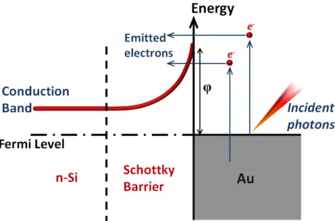
Figure 1.3: (a) Energy band diagram of n-type Si showing the conduction and valence bands. Absorption of an incident photon excites an electron from the valence band to the conduction band, leaving a hole in the valence band (band-to-band absorption). Only photons with energies (hν) greater than the energy bandgap (Eg) of Si are absorbed (hν > Eg) and can create electron-hole pairs. (b)
Energy band diagram of ideal Au/n-Si Schottky junction where the work function of the metal is aligned with the Fermi level of the semiconductor. Absorption of an incident photon excites an electron of the metal to higher energy levels and this highly energetic electron can be collected to the semiconductor over the Schottky barrier. Ideally the energy of the photon (hν) must be greater than the Schottky barrier height (ϕ), which is usually much smaller than the energy bandgap (Eg) of Si. In practice, even the photons with energies smaller than the
Schottky barrier height can contribute to the photocurrent.
In the internal photoemission process, the photons incident on a metal are absorbed by the metal and the absorbed photons transfer their energy to the electrons of the metal. The electrons of the metal are excited to the higher en-ergy levels in the metal with the enen-ergy they received from the absorbed photons and these highly energetic electrons are called “hot electrons”. Hot electrons travel with randomly oriented momenta in the metal and can be collected into a semiconductor to produce photocurrent in a metal-semiconductor Schottky junc-tion. The electrons are emitted over the Schottky barrier with the energy they have received from the absorbed photon, completing the internal photoemission process. Exploiting the hot electron generation mechanism in metals for detec-tion of sub-bandgap photons was demonstrated by Peters et al. in 1967 [9]. They
used an Au/n-Si Schottky barrier diode where the sub-bandgap photons were absorbed in the Au layer, generating hot electrons. The generated hot electrons are injected into the n-Si substrate and collected as photocurrent. Incident pho-ton to current conversion efficiency of this mechanism strongly depends on three factors: the absorption probability in the metal layer, the collection efficiency of the photogenerated hot carriers from the metal and the rate of regeneration of the lost electrons back to the metal. The collection efficiency of the hot electrons is mainly governed by the Schottky junction. The main mechanisms of the in-ternal photoemission process, the electrical properties of Schottky junctions and several factors that affect the charge collection mechanism at Schottky junctions are explained in Chapter 2.
Photodetection via the internal photoemission process has attracted great at-tention due to its simplicity, repeatability, low-cost and fabrication uniformity. However, the high reflection of metal surfaces has become the main drawback of this photodetection scheme. Electromagnetic waves at optical frequencies can-not properly penetrate into the metals used in Schottky barrier photodetectors. Hence, when photons are directly incident on a metal surface, a large portion of the incident photons are reflected back and only a small amount can propagate into the metal to be absorbed therein. Use of surface plasmons has emerged as a promising solution to this problem. In properly designed structures or optical configurations, surface plasmons can be excited on metal surfaces and the inci-dent optical energy can be tightly confined to the metal layer. Surface plasmons can then decay by giving their energy to the electrons of the metal, and excite the electrons to higher energy levels. This process is called surface plasmon assisted hot electron generation. Chapter 3 describes the use of surface plasmons for hot electron generation in Schottky barrier devices. The theory and applications of surface plasmon assisted hot electron generation process are discussed together with a brief review of surface plasmon literature.
Many researchers have worked on different approaches in order to make use of surface plasmon assisted hot electron generation and enhance the coupling of the incident light to the metal layer of the Schottky barrier devices. Akbari et al. used a metal stripe plasmonic waveguide on Silicon surface. A surface plasmon
polariton (SPP) mode, strongly confined to the metal semiconductor interface, is supported on this plasmonic waveguide [10, 11]. Knight et al. demonstrated optical nanoantennas on Silicon to collect the incident near infrared light and ex-cite surface plasmons to enhance the hot electron generation rate through surface plasmon decay [12]. Sobhani et al. achieved strongly resonant and narrowband photodetection in the infrared region of the spectrum with metallic gratings on Silicon [13]. The fabrication of the plasmonic structures used in such studies gen-erally requires high resolution photolithography techniques, which greatly limits the integration of this approach to commercial photodetectors. We form ran-domly distributed and ranran-domly sized Au nanoislands on Si substrate by rapid thermal annealing of a thin Au layer [14]. These nanoislands give broad-band plasmonic enhancement at the near infrared wavelengths and we demonstrate hot electron based photodetectors with photoresponsivity values on the same order as the narrow-band plasmonically tuned hot electron based photodetectors in the literature [12, 13]. Chapter 4 explains the device architecture of our hot electron based NIR photodetector and describes the experimental details including the de-vice fabrication, nanoisland formation, dark current–voltage measurements and photoresponsivity measurements. A theoretical analysis based on finite-difference time-domain (FDTD) simulations is also presented.
Use of Si substrates for hot electron based photodetection is preferred to achieve CMOS compatible fabrication of Schottky barrier photodetectors oper-ating at infrared wavelengths since the monolithic integration with the read-out circuitry is expected to substantially reduce the cost compared to the other in-frared detector devices based on InGaAs, HgCdTe or SiGe compounds. On the other hand, for photovoltaic and photocatalytic applications the use of single crys-talline Si substrates is still costly and limits large-area scalability. For hot electron based photovoltaic and photocatalytic applications, TiO2 appears to be the most
commonly used semiconductor material due to its large bandgap and high den-sity of states (DOS) in its conduction band, allowing fast electron injection [1]. Many studies have been conducted using Au or Ag nanoparticles combined with TiO2 semiconductors [15, 16, 17], and following these studies a variety of
nanotube arrays [18, 19], ZnO nanorods decorated with Au nanoparticles [20, 21], and coreshell SiO2–TiO2 nanoparticles decorated with Au nanoparticles [22]. On
the other hand, another approach utilizes metal-insulator-metal (MIM) junctions without incorporating any conventional absorber or semiconductor [23, 24]. In our hot electron based photovoltaic studies, we follow the second approach and focus on metal-insulator-metal (MIM) device architectures [25]. An MIM device can be fabricated on any substrate with a sufficiently flat surface such as glass; hence low-cost and wide-area fabrication is possible. Surface plasmon excita-tion on an MIM photovoltaic device was demonstrated in a study by Wang et al., where they used the Kretschmann configuration to excite surface plasmons at the MIM device fabricated on a prism and observed photovoltaic activity by increasing the absorption in one of the metal layers due to the highly localized surface plasmon mode [23]. The use of a prism for surface plasmon excitation is typically impractical for wide-area implementation of photovoltaic devices, hence different plasmon excitation schemes are necessary. In Chapter 5, we propose a double MIM structure for the excitation of plasmonic resonances under direct illumination. The device architecture is explained and the working principle of the device is supported with FDTD simulations and experimental results.
In addition to the use of surface plasmon excitation for hot electron based photodetection and photovoltaics, several groups have demonstrated the use of surface plasmon excitation on MIM structures for broad-band optical absorbers [26, 27, 28]. Nielsen et al. has shown that around 94% average optical absorption can be achieved in the visible wavelength range (400-750 nm) with an Au-SiO2
-Au stack [27]. Wadell et al. made an optical absorption engineering study with a nanodisc of Au-SiO2-Pd stack. They show that MIM plasmonic nanoantennas
incorporating Au as the metal layers can show strong resonance but this strong resonance alone is not enough for the efficient absorption of incident light. Hence they use an Au nanodisc to act as a plasmonic nanoantenna, which transfers the power to Pd nanodisc to be efficiently absorbed and dissipated [28]. An absorption engineering study is also possible for the double MIM device discussed in Chapter 5. We conduct FDTD simulations of this device architecture by using different metals and plasmonic structures, and investigate the optical absorption spectrum.
We show that careful design and material choice can allow the engineering of the absorption in such a structure. Narrow-band or broad-band resonances can be obtained and the optical absorption can be forced to occur mostly in the desired layer of the double MIM structure. The absorption spectrum can also be precisely tuned with the nanoantenna dimensions. The results of this absorption engineering study in double MIM structures are presented in Chapter 6.
Chapter 7 concludes this dissertation by briefly summarizing the results we have achieved with this study and gives future directions related to these topics.
Chapter 2
Hot Electron Based
Photodetection
2.1
Internal Photoemission
When a metal is in contact with a semiconductor surface, a potential barrier de-velops between the two materials and a Schottky junction is formed. The energy band diagram of a Schottky junction is shown in Fig. 2.1. The energy barrier formed at this junction is known as the Schottky barrier. In a hot electron based photodetection scheme, photoexcited electrons in the metal that can overcome this Schottky barrier are collected at the semiconductor. The collection of the photoexcited hot electrons at the semiconductor is the “internal photoemission process”.
The height of the Schottky barrier, ϕ, can be calculated as ϕ = ΦM − χ
where ΦM is the work function of the metal and χ is the electron affinity of
the semiconductor [9]. Hot electrons with energies greater than the Schottky barrier height, ϕ, can be emitted to the semiconductor if the required momentum condition is satisfied. Hot electrons with energies lower than the Schottky barrier height can still tunnel to the semiconductor but the probability of photoemission
Figure 2.1: Energy band diagram of an Au/n-Si Schottky junction. Photons incident on the metal can excite the electrons of the metal to higher energy levels (hot electron generation) and these hot electrons can be emitted into the semiconductor to generate photocurrent (internal photoemission).
is significantly reduced in such a case.
The photoemission current at a junction with Schottky barrier height ϕ can be expressed as [9]:
IS = A(hυ)2, hυ > ϕ + 3kT (2.1)
where h is the Plancks constant, υ is the frequency of the incident light and A is a constant that does not depend on υ. The Schottky barrier height can be deduced by plotting the square root of the photoemission current (IS) as a
function of photon energy (hυ) and extrapolating the linear region of the plot to the IS = 0 point. A fundamental study related to photoemission process was
conducted by Fowler [29]. The analysis in Fowlers study suggests that the change in different photoresponse spectra can be completely accounted for by the change of distribution of the electrons with the temperature. Namely, an electron with an initial energy Ex could be modeled as a “hot” electron with higher energy,
Ex+ hυ, after the photoexcitation of the electron by a photon with energy hυ.
This excess energy lets the electron travel in the metal with increased momentum and gives the electron the necessary energy to overcome the Schottky barrier if
the electron can reach the metal-semiconductor junction. If the electron cannot be injected to the semiconductor, the excess energy received from the absorbed photon is eventually lost to the lattice vibrations and dissipated as heat [23]. The maximum length that an electron can travel without losing its excess energy is named as “mean free path” and depends on factors like the metal type and the total energy of the hot electron [30, 31].
The efficiency of photodetection via the internal photoemission process is typi-cally low. Main limitations are the optical properties of metals (light penetration is low), the relatively short mean free path of hot electrons in metals (typically 10s of nms), the Schottky barrier height and the other electrical properties of the Schottky junction. These limitations bring an important design challenge that involves the thickness and optical properties of the metal, and requires careful optimization of the electrical properties of the Schottky junction.
2.2
Metal-Semiconductor (MS) Schottky
Junc-tion
The electrical properties of the Schottky junction are mainly governed by the electron affinity and Fermi level of the semiconductor and the work function of the metal. As shown in Fig. 2.1, at thermal equilibrium the work function of the metal and the Fermi level of the semiconductor are aligned at the same energy level. The energy difference between the electron affinity of the semiconductor and the work function of the metal has to be preserved at the metal-semiconductor junction and this difference sets the height of the potential energy barrier from the metal to the semiconductor (ϕ = ΦM−χ). Since the Fermi energy of the semiconductor
is smaller than the work function of the metal (EF < ΦM), alignment of the Fermi
level and the metal work function forces the energy bands of the semiconductor to be bent upwards at the junction, creating a built-in electric field from the bulk of the semiconductor to the metal. This electric field can be utilized to separate the electron-hole pairs that are generated in the semiconductor. Use of Schottky
diodes as photodetectors and solar cells rely on this mechanism to collect the photogenerated charge carriers in the semiconductor.
The choice of the direction of the built-in electric field has a crucial effect on the dark current performance of the Schottky diode. The majority carriers, in this case the electrons, of the n-type Si in Fig. 2.1 can not flow to the metal hence their contribution to the current is significantly reduced. This potential barrier is the main reason a voltage develops between the metal and the semiconductor upon optical illumination. When a metal with much smaller work function is in contact with the same semiconductor, the energy bands will bend downwards, resulting in a very small or no potential barrier, hence an ohmic contact. The dark current will substantially increase, making such a junction impractical for photodetection. Since there will be no potential barrier to stop the backflow of electrons, no voltage will build up upon optical illumination.
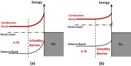
Ideally, one can engineer such electrical properties of a Schottky junction by choosing different types of metals and semiconductors. This simple approach, however, does not always give sufficiently correct results in practice. When a metal and a semiconductor are in contact with each other, the work function of the metal might be “pinned” to an energy level at the semiconductor junction (Fig. 2.2). The pinning level of the metal work function severely affects the Schottky barrier height and cannot be predicted by theoretical calculations [32]. Work function pinning can be avoided by using a very thin interlayer dielectric between the metal and the semiconductor [33]. The presence of such an interlayer dielectric layer has a significant effect on the electrical properties of the Schottky junction.
Figure 2.2: Energy band diagrams of Au/n-Si Schottky junctions without the work function pinning (a) and with work function pinning (b). The height of the Schottky barrier is directly affected by the pinning of the work function to another level. The shape of the Schottky barrier and other electrical properties are also affected by this change in the work function.
2.3
Metal-Insulator-Semiconductor (MIS)
Junc-tion
As well as changing the pinning of the work function, use of an interlayer dielec-tric will also directly affect the tunneling probability at the Schottky junction. The direct tunneling probability depends on the thickness of the interlayer di-electric and the height of the potential barrier introduced by the didi-electric ma-terial [34]. At high bias voltages, the energy bands will be bent at the Schottky junction and the potential barrier introduced by the dielectric layer will get a triangular shape at sufficiently high electron energies. This triangular shape of the potential barrier actually implies a thinner potential barrier for the electrons with higher energies and the tunneling process through such a potential barrier is called Fowler-Nordheim tunneling. The electron reaches the conduction band of the insulator by tunneling part of the potential barrier. The direct tunneling and Fowler-Nordheim tunneling mechanisms are depicted in Fig. 2.3 [35].
Figure 2.3: The energy band diagram of a metal-insulator-semiconductor (MIS) junction (a) at flat-band condition and (b) under reverse bias. In the direct tun-neling process (green arrows) the tuntun-neling probability depends on the thickness and the height of the potential barrier, and it is relatively independent of the bias voltage. For the electrons with sufficiently high energies, Fowler-Nordheim tunneling is observed (red arrow). The effective insulator thickness is reduced due to the bending of the energy bands with the high electric field. The tunneling probability depends on the electron energy and the bias voltage.
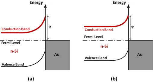
can greatly change the shape of the Schottky barrier. Effective thickness of the Schottky barrier changes due to the bending of the conduction and valence bands (Fig. 2.4). Tunneling probability of the hot electrons with energies smaller than the Schottky barrier is also affected by the change of the Schottky barrier shape. However, one must note that the tunneling current is almost negligible compared to the current generated by the internal photoemission over the Schottky barrier.
2.4
MIS Solar Cells
Schottky barrier diodes are also used in photovoltaic applications by making use of the built-in electric field to collect the photogenerated electron-hole pairs in the semiconductor. Usually an interlayer dielectric layer is used in order to avoid the work function pinning and to suppress the dark current. This section investigates the voltage development and dark current generation mechanisms at MIS solar
Figure 2.4: Energy band diagrams of two Schottky junctions with (a) highly doped and (b) lowly doped semiconductors. Band bending is greater for the highly doped semiconductor (a) compared to the lowly doped semiconductor (b) due to the position of the Fermi level. The triangular shape of the barrier gets thinner as the band bending increases, resulting in an increase in the tunneling probability of the hot electrons at these energy levels (Fowler-Nordheim tunneling).
cells to provide more insight into the electrical properties of Schottky junctions. In general, the power conversion efficiency of a solar cell can be expressed as:
η = IscVocF F Pina
(2.2) where Isc is the short circuit current, Voc is the open circuit voltage, F F is the
fill factor, Pin is the incident solar power density and a is the surface area of the
solar cell.
The open circuit voltage, Voc, of metal-semiconductor junction solar cells
suf-fers severe degradation due to high dark current and this seems to be the main bottleneck for the Schottky barrier solar cells. The total dark current density in a Schottky junction can be expressed as [36]:
JD = Jth+ Jrg + Jd+ Js (2.3)
where the dark current components are [36]:
emission of charge carriers into the metal.
2. The recombination-generation current density, Jrg current due to the
gen-eration of electron-hole pairs in the depletion layer of the semiconductor. It should be noted that a depletion layer may not be present depending on the doping concentration of the semiconductor and the work function of the metal.
3. The injection-diffusion current density, Jd injection/diffusion of minority
carriers into the semiconductor bulk.
4. The surface states current density, Js current due to charge exchange via
surface states between the metal and the semiconductor.
Figure 2.5: Dark current mechanisms in a Schottky junction are shown on the energy band diagram of a forward biased metal-insulator-semiconductor (MIS) solar cell. The thermionic emission dark current, Jth, recombination-generation
current, Jrg, injection-diffusion current, Jd, and surface state current, Js, are
depicted on the energy band diagram. The thermionic emission dark current has been reported as the dominating dark current component for most practical cases.
Fig. 2.5 demonstrates these dark current components on the energy band dia-gram of an MIS junction with p-Si semiconductor, where the holes are the major-ity carriers [36]. Among these dark current components, the thermionic emission dark current is the dominant component for most cases. An expression for Jth
can be written as [34]:
Jth= ΘA∗∗T2exp(−qφb/kT ) exp(qVj/nkT ) (2.4)
where Θ is the majority carrier tunneling coefficient, A∗∗ is the Richardson’s constant, q is the electron charge, φb is the barrier height at zero bias voltage,
k is the Boltzmann constant, T is the temperature and n is the ideality factor. In traditional intimate contact metal-semiconductor Schottky barrier diodes φb is
relatively small due to the pinning by the surface states at the interface and this results in very high Jth values that are not suitable for photovoltaic applications.
By introducing a thin insulator layer at the interface, the semiconductor surface states can be passivated and φb will be dictated by the work function of the
metal. This allows considerable reduction of the thermionic emission dark current by proper choice of metal type. Reducing the thermionic emission dark current by increasing the insulator thickness and reducing the majority carrier tunneling coefficient, Θ, is also possible. However, such an approach is likely to degrade the solar cell efficiency since the tunneling probability of photogenerated charge carriers will decrease as well [36].
Inevitably, there is a trade-off between the open circuit voltage and the short circuit current of the Schottky junction as the interlayer thickness changes, and this presents another parameter to optimize the Schottky junction [37].
In addition to an interlayer dielectric, several different metal layers can be used to obtain the desired optoelectronic properties at the Schottky junctions. Au is commonly preferred as the absorber layer for its optical properties and long mean free path of hot electrons in Au [10, 12, 30]. Commonly a thin adhesion layer such as Ti is deposited prior to Au evaporation. This layer improves the adhesion of Au to the underlying layer and helps the formation of a continuous Au layer [12]. The work function of the metal layer in contact with the semiconductor is mainly governed by this adhesion layer, resulting in Ti/Si Schottky barrier properties in
the electrical characterization instead of Au/Si Schottky barrier characteristics [12, 36]. Similarly, a barrier metal layer is used when there is need to control the Schottky barrier height by choosing a metal with desired work function. An additional metal layer (contact metal) with high conductivity can also be used on the barrier layer to get low resistance electrical contact to the metal layer of the Schottky junction.
2.5
Conclusion
Despite the challenges in optimizing the Schottky junction for specific optoelec-tronic applications, Schottky junctions have been successfully used in photodetec-tion due to their simple fabricaphotodetec-tion, ease-of-integraphotodetec-tion to Si CMOS technology, repeatability and large area uniformity [38, 39]. The response times of Schottky barrier diodes are also typically much shorter than p-n junction diodes due to the lack of minority carrier storage effects. Response times as low as 10−10 seconds were reported in the earliest demonstrations of Schottky barrier infrared photode-tectors [9]. Schottky diodes have also been used for photovoltaic applications to simply introduce a built-in electric field to Si and collect the photogenerated electron-hole pairs in Si. Up to 8% − 10% power conversion efficiencies have been reported with this approach [36, 40]. The main challenge, which has been investigated for over a decade, is the low optical absorption of metals for hot elec-tron based photodetection and photovoltaic schemes. Use of surface plasmons to address this issue is explained in Chapter 3.
Chapter 3
Surface Plasmon Assisted Hot
Electron Generation
3.1
Introduction
When a light wave is directed at the interface between a metal and a dielectric, the oscillations of the electrons at the surface of the metal may match the oscillations of the electromagnetic field if certain conditions are satisfied. The light wave resonantly interacts with the mobile electrons at the surface of the metal and this resonant interaction induces density waves of electrons which are called surface plasmons. The frequency of the surface plasmon wave is the same as the frequency of the incident light wave, but the wavelength of the surface plasmon is much shorter. Possible applications that could be enabled by this property of light, such as using nanoscale plasmonic interconnects to carry information in a processing unit, resulted in a continuously increasing interest in this field [41]. Use of surface plasmons to improve the efficiency of photodetectors, solar cells and light emitting diodes (LEDs) [42, 43, 44], or the medical applications that use the enhanced local electromagnetic field created by the surface plasmon resonances [45] were quickly demonstrated. With the advances in computational power and novel numerical methods scientist can now accurately simulate the complex electromagnetic fields
generated by plasmonic effects. Invention of novel methods for nanofabrication, imaging and characterization also greatly accelerated the development of this field of research.
In properly sized metallic nanoparticles, the free electrons of the metal can oscillate with the same frequency as the incident light and resonate with the op-tical wave. This resonance, which is called localized surface plasmon resonance (LSPR), may give rise to strong, highly localized electromagnetic fields. Propa-gating modes of surface plasmon polaritons (SPP) can also be triggered on metal dielectric interfaces with properly designed phase matching techniques (Fig. 3.1) [46]. SPPs are dispersive electromagnetic waves coupled to the electron plasma of the metal. LSPRs on the other hand are non-propagating and arise due the coupling of the electromagnetic wave to the conduction electrons of metal nanos-tructures [47].
Figure 3.1: Propagating surface plasmon polaritons (SPP) and localized surface plasmon resonances (LSPR) at metal dielectric interfaces. SPPs can be excited by using a prism or with corrugations on the surface, and they propagate along the metal-dielectric interface. LSPRs are non-propagating and can be excited on metallic nanoparticles or metallic gratings even under direct illumination.
Integration of plasmonic resonance schemes with conventional photodetectors and photovoltaic devices by making use of the optical trapping and field concen-trating properties of surface plasmons has been studied extensively [43]. Typi-cally, such nanostructures are used as optical nanoantennas by placing them on or very close to the active region of an optical device. Even more interestingly, re-cent studies have also showed that such metallic nanoparticles and nanostructures can be used to directly convert the energy of electromagnetic waves to electrical energy by generating hot electrons in the metal by the decay of surface plasmons
[1, 23].
3.2
Localized Surface Plasmon Resonances
The interaction of an electromagnetic field with a sub-wavelength nanoparticle of size d, can be solved with quasi-static approximation provided that the size of the nanoparticle is much smaller than the wavelength of the electromagnetic field (d λ). In quasi-static approximation the phase of the electromagnetic field is assumed to be constant over the particle volume. The problem is simplified to a particle in static electric field, and the harmonic time dependence can be added once the field distributions are solved for the static case. This approach has been used to model the optical properties of metals accurately for nanoparticle dimensions less than 100 nm [47].
Solving the Laplace equation for the potential, ∇2Φ = 0, for a nanoparticle
in static electric field, E0 = E0z, we can calculate the resulting electric fieldˆ
distribution E = −∇Φ. For the simple case of a spherical nanoparticle with the dielectric function ε(ω) and radius a, and a non-absorbing and isotropic sur-rounding medium with the dielectric constant εm, the potential distribution can
be solved as: Φin(r, θ) = ∞ X l=0 AlrlPlcos(θ) (3.1) Φout(r, θ) = ∞ X l=0 [Blrl+ Clr−(l+1)]Plcos(θ) (3.2)
where Φin(r, θ) and Φout(r, θ) are the electric potential distribution inside and
outside the spherical nanoparticle, respectively. Pl(cos θ) are the Legendre
Poly-nomials of order l, and θ is the angle between the position vector r and the z-axis. The coefficients Al, Bl and Cl can be found by imposing the boundary conditions
at r = a and r → ∞. The potentials can then be written as [47]: Φin = −
3εm
ε(ω) + 2εm
E0r cos θ (3.3)
Φout= −E0r cos θ +
ε(ω) − εm
ε(ω) + 2ε E0a
3cos θ
A very fundamental result of Eq. 3.4 is the interpretation of this potential as the superposition of the applied field and the field of a dipole located at the center of the nanoparticle. Basically, in addition to the potential due to the applied electric field, another potential arises since the applied field creates a dipole at the nano-sphere. Rewriting the potential Φout we can get an expression for the
dipole moment p.
Φout = −E0r cos θ +
p · r 4πε0εmr3 (3.5) p = 4πε0εma3 ε(ω) − εm ε(ω) + 2εm E0 (3.6)
We can then define polarizability function, α, by using the equation p = εmε0αE0.
α = 4πa3 ε(ω) − εm ε(ω) + 2εm
(3.7) polarizability function α has a complex value and is a measure of how strongly a dipole can be created at the nano-sphere under quasi-static approximation. The denominator of the polarizability function α gives the Fr¨ohlich condition Re[ε(ω)] = −2εm, which gives a resonant enhancement. This condition holds
when the imaginary part of the dielectric function of the nano-sphere, Im[ε(ω)], is small or a slowly varying function of frequency. This resonance condition also implies that the maximum value of the polarizability function α is mainly limited by the imaginary part of the dielectric function of the nano-sphere, Im[ε(ω)], which corresponds to the optical losses in metals [47].
Calculating the electric field distribution inside and outside the nano-sphere, we observe that resonant enhancement occurs for both fields. Electric fields both inside the nanoparticle and in close vicinity of the nanoparticle are enhanced by the localized surface plasmon resonances. More commonly, resonant enhancement of Eout is exploited in photodetectors, biological and chemical sensors [48], and
surface enhanced Raman scattering (SERS) [49] to obtain highly confined electric fields in the near field of a nano-sphere. On the other hand, if the nanoparticles were to be used as hot electron generation spots in a surface plasmon assisted hot electron device, the field inside the nanoparticle would gain more importance.
Ein =
3εm
ε(ω) + 2εm
Eout = E0+
3n(n · p) − p 4πε0εm
1
r3 (3.9)
Having obtained the field distribution for the electrostatic case, we can calculate the electromagnetic field radiated by the nano-sphere upon illumination with a plane wave, E(r, t) = E0e−iωt, by introducing a harmonic time dependence to the
dipole moment calculated by the quasi-static approach.
p = εmε0αE0e−iωt (3.10)
where α is the same polarizability function that is calculated for the electrostatic case. The radiation of this dipole represents the scattering of the plane wave by the nano-sphere and can be investigated as the radiation of a point dipole. The scattering cross section, Csca, and the absorption cross section, Cabs, can be
written as follows [50]: Csca = k4 6π|α| 2 = 8π 3 k 4a6| ε(ω) − εm ε(ω) + 2εm |2 (3.11)
Cabs = kIm[α] = 4πka3Im[
ε(ω) − εm
ε(ω) + 2εm
] (3.12)
These cross sections correspond to the efficiency of the metal particle for scatter-ing and absorption of light. It is also important to note that for nanoparticles much smaller than the wavelength, the efficiency of absorption scales with a3 and
dominates over the efficiency of scattering which scales with a6 [47].
This approach to calculate the polarizability of a nano-sphere under quasi-static assumption can be extended to ellipsoid nanoparticles and the effect of their extended shape on the polarizability can be investigated. It has been shown that the resonance on the longer axis of such structures exhibit a significant red-shift compared to a nano-sphere of the same volume [47]. For particles with larger dimensions, an electrodynamic approach is required since the phase of the incident field changes considerably over the volume of the particle. This approach is now known as the Mie theory and can completely describe the scattering and absorption of electromagnetic radiation by a sphere [47, 51].
The formulation of the polarizability of nanoparticles with spherical or ellipsoid shapes also leads us to decay mechanisms of surface plasmons. Two main decay