Differential evolution algorithm
based photonic structure design:
numerical and experimental
verification of subwavelength λ/5
focusing of light
E. Bor
1,2, M. Turduev
2& H. Kurt
1Photonic structure designs based on optimization algorithms provide superior properties compared to those using intuition-based approaches. In the present study, we numerically and experimentally demonstrate subwavelength focusing of light using wavelength scale absorption-free dielectric scattering objects embedded in an air background. An optimization algorithm based on differential evolution integrated into the finite-difference time-domain method was applied to determine the locations of each circular dielectric object with a constant radius and refractive index. The multiobjective cost function defined inside the algorithm ensures strong focusing of light with low intensity side lobes. The temporal and spectral responses of the designed compact photonic structure provided a beam spot size in air with a full width at half maximum value of 0.19λ, where λ is the wavelength of light. The experiments were carried out in the microwave region to verify numerical findings, and very good agreement between the two approaches was found. The subwavelength light focusing is associated with a strong interference effect due to nonuniformly arranged scatterers and an irregular index gradient. Improving the focusing capability of optical elements by surpassing the diffraction limit of light is of paramount importance in optical imaging, lithography, data storage, and strong light-matter interaction.
Light interaction with an absorption-free medium can experience reflection, refraction, diffraction, and coherent or incoherent scattering1. Conventional optical materials and structures manipulate light propagation with a limited capability. For example, total-internal reflection-based light guidance in fiber optic cable or integrated optical waveguides is only one type of light confinement mechanism deployed. It was only recently that multidi-mensional periodic variation of the refractive index with a strong contrast ratio provided an energy band gap con-cept similar to the electronic band gap occurring due to the interaction of electron movement with the periodic potentials of atoms in crystalline solids. The forbidden energy interval is closely linked with Bragg scattering. As a result, tailoring light propagation with a photonic band gap mechanism has resulted in photonic crystal wave-guides and photonic crystal fibers2.
Photonic crystals (PC) are periodically designed artificial structures that manipulate the flow of light, and their periodicity can be one, two, or even three dimensional2. PCs have many remarkable properties that make it indispensable to control the photon movement using structures such as waveguides3, cavities4, bio-chemical sensors5, flat lenses6, and low-threshold lasers7. Photons may also be trapped or emitted using a single defect8.
Even though there are various light manipulation scenarios, one of the widely targeted problems is to improve focusing characteristics of photonic structures. The wave nature of light dictates the limitation to focus light below a certain spot size smaller than half of the wavelength of light. A common way of focusing light requires either mirrors or lenses with curved surfaces and constant refractive indices1. Reflection and refraction are responsible for bringing light into focus in these cases. Meanwhile, one can use a diffraction mechanism to focus incident 1Department of Electrical and Electronics Engineering, TOBB University of Economics and Technology, Ankara,
Turkey. 2Department of Electrical and Electronics Engineering, TED University, Ankara, Turkey. Correspondence and
requests for materials should be addressed to E.B. (email: [email protected]) received: 14 April 2016
Accepted: 08 July 2016 Published: 01 August 2016
OPEN
or very small biological particles such as DNA, viruses, and proteins. A dielectric PC slab has been used to achieve canalization for focusing light at the subwavelength scale with a full width at half maximum (FWHM) value of 0.059λ022. In that study, the main purpose is to transport the focal point to long distances. However, the focusing property of the structure for short distances is not considered and there occurs strong reflection at the interface between air and structure. Hypergratings are demonstrated to obtain FWHM values between λ0/20 and λ0/5023. In ref. 24 planar anisotropic metamaterial with zone plates is introduced for the purpose of subwavelength focus-ing of light where the calculated FWHM value of focal point is equal to λ0/10. However, metamaterial structures suffer from high material absorption losses due to the imaginary part of the metalic material permittivity. In the case of the focusing by metamaterial structures, absorption also affects the focal point resolution that limits the subwavelength focusing performance of the structure. Additionally, off-axis focusing characteristic in subwave-length scale by nanoscale slits with metamaterial slab is reported where the FWHM value is equal to 22 nm at the operating wavelength of 365 nm. That corresponds to a FWHM value to be approximately 0.060λ025. In this case, because of the material losses inside the structure, the intensity of focused light is very low compared to the source light. The phase compensation mechanism is proposed for focusing the plane wave to a spot by construc-tive interference in a metamaterial with FWHM value of 0.14λ026. Also, an optical hyperlens system is proposed that has resolution capabilities better than λ0/227. An important question can be asked: what would happen if an optimization algorithm is utilized to design all dielectric structure to obtain subwavelength focusing of light?
Designing different and complex photonic structures based on theoretical knowledge and an intuition approach is limited. For this reason, a variety of optimization algorithms have been used to design efficient pho-tonic integrated structures. A genetic algorithm was used to design a spot size converter, lenses, a demultiplex coupler and a large photonic band gap structure13,28–30. The same algorithm was also used to generate different orders of Hermite–Gauss profiles31. In addition, topology optimization was applied to obtain a photonic band gap and design a waveguide bend, mode converter, and subwavelength focusing structure32–35. Another optimi-zation technique called particle swarm optimioptimi-zation was used to obtain directional emissions at the exit of the PC waveguide and engineer slow light parameters of a line defect waveguide36. An algorithm based on convex optimization was applied to design a wavelength demultiplexer37. Also, a nonlinear search algorithm was recently used to design a beam-splitter38, a gravitational search algorithm to design a nanophotonic cavity39, and the direct binary search algorithm to design optical diodes40,41.
In the present work, we introduce a differential evolution (DE) algorithm to design a subwavelength focusing PC structure composed of all dielectric scattering elements. As we demonstrate later, the transverse cross section of the input beam was shaped by the designed photonic structure. We achieved strong focusing of the beam with carefully controlled side lobe intensity levels. Microwave experiments were performed to verify the numerical results.
In the following parts of the paper, we outline the implementation of the DE algorithm to design a lens for subwavelength focusing. The distance between the dielectric rods was optimized to achieve strong light focusing. The results show that the proposed optimization strategy can be used to design a subwavelength focusing PC with desired beam properties via defining multiobjectives. The proposed approach possesses some advantages. For example, all dielectric materials are utilized. There are no metallic or exotic materials deployed in the design. As a result, the subwavelength focusing structure is inherently free from absorption loss and can work for a broad wavelength interval.
Definition of the problem and design approach of algorithm
The main aim of the proposed work was to find a desired photonic structure that resulted in subwavelength focus-ing of the illuminatfocus-ing wave. The relevant parameters for the most critical characteristics of a focusfocus-ing apparatus are the spatial size and the cross-sectional profile. These geometric properties are important for different applica-tions such as beam size shaping, high resolution imaging, and the high efficiency of light coupling. The size of the focal spot is characterized by the FWHM value, and for subwavelength focusing it should be smaller than λ /2 in air. While considering the strong light focusing below λ /2, one has to pay attention to the emergence of side lobes, which should not carry a large amount of the beam’s energy.
If a large amount of the energy is shared with the side lobes, then an undesired radiation pattern may emerge after propagating a certain distance, and the interaction of light with the medium at the focal spot would become weaker. When the side lobes of the focal point are reduced, the FWHM of the main lobe (focal spot) is usually increased. There is a trade-off to be solved in the present work. In order to consider not only a small FWHM
but also fairly suppressed side lobes compared to the main lobe, multiobjective optimization can be utilized as a possible solution.
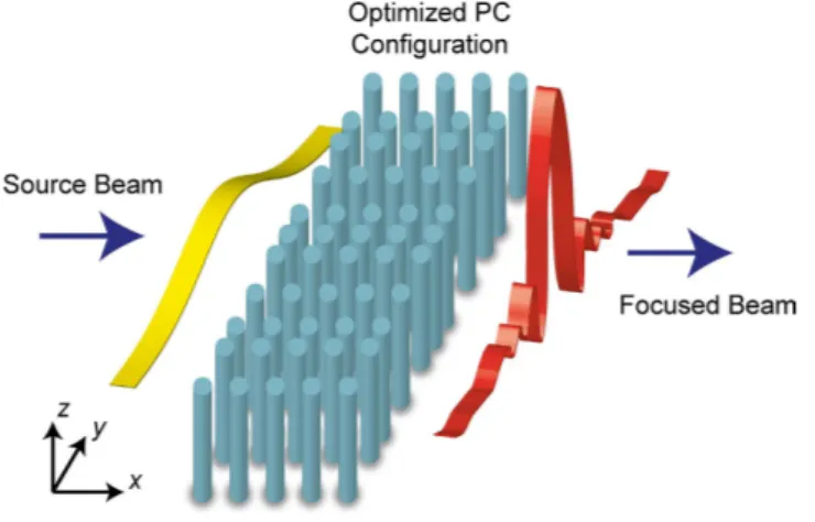
Figure 1 pictorially outlines the design approach implemented in the DE algorithm. The intensity profiles of the incident and transformed beams are figuratively presented. Our purpose is to use the DE algorithm to opti-mize the beam shaping structure.
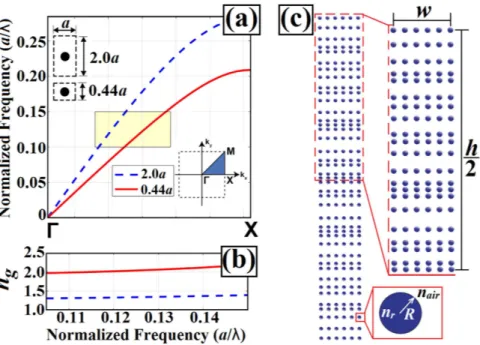
In this study, the filling ratio/effective index of the PC structure was modulated and optimized using the DE algorithm to obtain a strong focusing effect. Refractive index modulation can be achieved by engineering the PC parameters, such as gradually changing the material index, filling factor and/or lattice period42–44. Moreover, index modulation can also be accomplished by introducing different duty cycles that locally modulates the effec-tive index of refraction in subwavelength gratings45,46 and inhomogeneous grating structures with lensing effect47. In the current work, we utilized the last method, where size optimization of the PC unit cells was performed while keeping the material type and rod radii the same. The adjustment of the size of the PC unit cells resulted in a modulation of the effective index of refraction, which allowed the structure to manipulate phase fronts of the propagating wave. The radii of the PC rods were fixed at 0.20a, and their refractive indices were kept at n = 3.13. (The PC rods were considered alumina rods for the microwave experiment). The lateral dimension of the unit cells ranges from Δ y = 0.44a to Δ y = 2.0a according to the optimization. The lattice constant is represented by a. Moreover, the distance between rods along the propagation x-direction is fixed to 1a (i.e., the modulation of the effective index performed along only the transverse y-direction). Corresponding variations of cell sizes in trans-verse y-direction are depicted in the Fig. 2a as an inset. It should be noted that there is a restriction on the place-ment of dielectric rods. The maximum distance between the centers of PC rods in the same column is 2.0a. Since the diameter of each rod is 0.40a, the minimum distance between adjacent rods in y-direction should be greater than 0.40a so they do not touch each other. For this reason, the minimum distance was fixed at 0.44a. Using these structural parameters, we calculated the dispersion diagrams of PC unit cells with maximum and minimum lateral sizes by exploiting the plane wave expansion (PWE) method in the frequency domain48. The dispersion diagram is shown in Fig. 2a. The related bands move to higher frequencies while the unit cell size increases (the lateral dimension increases and the longitudinal dimension is kept constant). We should note that throughout all numerical analyses, only transverse magnetic (TM) polarization was employed, where the concerned nonzero electric and magnetic field components are Ez, Hx, and Hy, respectively. Additionally, we designed the photonic
structure operating in the first band.
The group indices of each band (ng) were extracted using the slope information of the relevant curves
pre-sented in Fig. 2a, and the result is illustrated in Fig. 2b. For the longer wavelengths in the first band, the curves are closely spaced and deviate in a linear manner with respect to the normalized frequency. The calculated group indices within the normalized frequencies a/λ = 0.10 to 0.14 cover values between 1.40 and 2.20. It can be con-cluded that different values of Δ y provide specific ng values within the spectral window.
After determining the initial conditions of the approach, the DE optimization algorithm was incorporated into the design for subwavelength focusing. DE is a metaheuristic method to provide a sufficiently good candi-date solution to multiobjective optimization problems. Since DE does not search the complete design space, the obtained solution is not the best solution but one of the efficient solutions that satisfy the intended conditions for the optimization problem under study. Cost function, which is part of DE and necessary for convergence, should be designed carefully in order to find a good solution49. In our designs, we applied the “best/1/bin” method of DE. At the beginning of the optimization, the algorithm randomly generated a population of a certain number of PC structures, called individuals. Each individual, with its own cost value, was made of a fixed number of parameters (i.e., the distances between PC rods). Individuals with better cost values were selected to generate the population of the next iteration. The algorithm ends when the defined cost value of any individual satisfies the desired termi-nation condition or when the maximum number of iterations which is defined at the beginning of the algorithm is reached.
As explained above, the DE was applied to optimize the distances between dielectric rods (i.e., the lateral size of the unit cell in a column). Since an objective of the proposed work was also to generate a compact and feasible Figure 1. Schematic representation of the strong light focusing problem. Dielectric PC rods with the constant refractive index nr = 3.13 are placed in an air background with the refractive index nair = 1.0.
PC structure, one should define the structural restrictions. Hence, the maximum distance between the centers of rods in the same column is 2.0a, and the minimum distance is 0.44a. To obtain the focal point at the optical axis, we used mirror symmetry with respect to the x-axis. As a result, the algorithm was run to generate only half of the structure, and that half was duplicated symmetrically to obtain the complete configuration. Moreover, the cost function was defined to minimize the FWHM value and suppress the intensity level of the maximum of side lobes (MSL) to stay under 20% of the normalized arbitrary value of the intensity profile at the focal point. We set the desired value for FWHM close to zero since the lowest possible FWHM value was targeted for subwavelength focusing. At the beginning of the algorithm, the number of columns and the normalized frequency were defined by the user. Furthermore, to see the effect of the longitudinal size of the optimized PC structure on focusing ability, we applied DE for a different number of columns as the values varied from 5a to 10a for each design frequency. One more important parameter is the distance between the focal point and back surface of the PC structure. In our optimization, we calculated the FWHM values at least 0.32a distance away from the end of the structure. The cost function is mathematically defined in equation (1):
α α
= − + −
f x y( , ) x x xd yy yd (1)
where xd and yd are the targeted FWHM and desired MSL values, respectively. Variables αx and αy are the
weight-ing factors that balance the effect of FWHM and MSL values to the value of the cost function.
Numerical Results
Numerical modeling of the optimized PC lens and its time-domain analysis were realized using the finite-difference time-domain (FDTD) method50,51. In all numerical simulations, the computational domain was restricted to a 2D spatial domain and the third dimension was taken to be uniform. To eliminate undesired back reflections, the boundaries of the computational domain were surrounded by perfectly matched layers52. A con-tinuous source with a Gaussian profile was utilized to calculate the spatial intensity distribution of the focusing effect of the optimized PC lens.
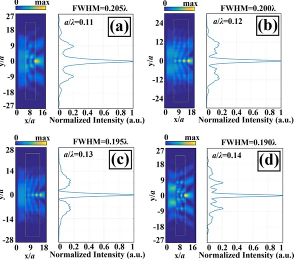
The algorithm was applied to design different structures for different normalized frequency values. For each normalized frequency, different numbers of columns were chosen to design photonic structures. The schematic view of the optimized PC structure is presented in Fig. 2c. An optimized PC lens with a better cost value was selected from among the structures designed with the same normalized frequency value. Therefore, the number of columns in selected PCs was varied independently from the normalized frequency values. In Fig. 3, intensity distributions and cross sections of the field at the focal point are given. Related figures of PCs with normalized frequency values a/λ = 0.11, 0.12, 0.13, and 0.14 are shown in Fig. 3a–d, respectively.
As the results show in Fig. 3, subwavelength focusing down to FWHM = 0.19λ was achieved. The other FWHM values were below 0.50λ as well. Also, it is clear that the side lobes were symmetrical with respect to the
x-axis. The FWHM and MSL values were calculated, and the results of the structures satisfy the desired conditions
of DE. In general, we obtained around λ/5 FWHM values and reduced maximum side lobe levels to under 20% of the maximum value of 1.0 for each PC. Moreover, the spot-size conversion ratio of each selected structure was calculated. The results are summarized in Table 1.
Figure 2. (a) Dispersion curves of rectangular cells with different dimensions. (b) Group index curves for the two extreme cases corresponding to the smallest and largest cells. (c) The DE generated two-dimensional photonic crystals.
We should point out that while subwavelength focusing was achieved with the suppressed side lobes, we strictly pushed the level of the side lobes to stay below a certain value. Moreover, the calculated values of the energy fraction of main lobe are given in Table 1. As it is seen from the results, around 40% of overall energy is concentrated within the main lobe of the focused beam.
For the four different designed structures which are presented in Fig. 3, FWHM values at different focal dis-tances are numerically calculated and FWHM dependence on focal disdis-tances is given as plots in Fig. 4. As can be seen from the figure, focal distances are varied from 0.32a to the 2.56a away from the structure with 0.32a steps for all four different structures. Furthermore, to show the transverse cross-sectional intensity profile variation in terms of focal distance values of 0.32a and 2.56, we included insets for each designed structure in Fig. 4a–d. As it is seen from Fig. 4, the variations of the FWHM values with increasing of focal distance values are nearly linear and FWHM values stay under the diffraction limit for greater values of focal distances increasing from 0.32a to 2.56a. Even though the level of side lobes increase as focal distance increases, MSL values stay suppressed under the 50% of the normalized intensity at each focal distance value.
One can argue that two physical mechanisms govern the strong focusing of light. The first one is the rather irregularly placed dielectric rods providing an index gradient. Although there is irregular spacing between dielec-tric locations, as shown in Fig. 2c, the overall density of dielecdielec-tric material is higher at the center of the structure Figure 3. Different photonic structures generated by implementing the algorithm. (a) Steady state intensity profiles at a/λ = 0.11 for the structure with 6 columns. Similar plots (b) at a/λ = 0.12 for 10 columns, (c) at
a/λ = 0.13 for 10 columns, and (d) at a/λ = 0.14 for 6 columns.
Normalized
Frequency (a/λ) Number of Columns FWHM Maximum Side Lobe Level Conversion RatioSpot-Size Fraction of Energy of Main Lobe
0.11 6 0.205λ 0.199 9.34 56.69%
0.12 10 0.200λ 0.168 12.08 41.35%
0.13 10 0.195λ 0.148 12.62 43.87%
0.14 6 0.190λ 0.199 12.95 39.79%
and decreases toward the edges. The indication of the index gradient can be seen in the phase front changes apparent in the intensity profiles, as shown in Fig. 3.
The other mechanism is based on the interference of light at structure places that have a wide distance between rods. These places guide light and promote multibeam interference. An electric field exists at the exit of each waveguide channel, and the interference of waves emanating from the N-channel provides a total scalar electric field in the form of the following expression:
∑
= ϕ ω = − ⋅ E U e e (2) sum i N i j j t k r 1 ( ) ( (i i i))In equation (2), the amplitude and phase of the field at the exit side of the waveguide are represented by Ui and φi, respectively. Also ω and N represent radial frequency of propagating wave and number of channels, respectively. Time harmonic dependency is assumed in the equation. The phase term contributing to the interference effect for each channel is determined by the dot product of the wave vector, ki, and the position vector, ri. The intensity profile is determined by (E Esum sum⁎ )/2 where Esum⁎ is complex conjugate of the total electric field. Obtaining a closed form expression for the intensity profile without any approximation or assumption for the above equation is not straightforward. However, we can point out that the parameters that play roles for the intensity profile are amplitude profiles, relative phase terms, and the number of interfered waveguides. A large N yields a narrower peak at the central part of the structure with a higher intensity value. In other words, as N increases, the central lobe concentrates more tightly due to the increased number of waveguide channels. The presence of the side lobes is also an indication of a multibeam interference effect. As a result of these two phenomena, strong focusing of the beam occurs at the outside of the structure. Since we do not know the phase difference between each fictitious channel and amplitudes of the wave at the exit of the structure, we do not attempt to derive an intensity distribu-tion profile at the back side of the structure. We solely share that equadistribu-tion in order to discuss the importance of the nonuniformly distributed amplitudes and phase variation at the end of the structure that plays role for the focusing effect.
Experimental Results
To verify the numerical results, we performed experimental realization at the microwave region. We used die-lectric alumina rods to generate the PC lens, as in the numerical calculations. Figure 5a shows the schematics and photographic illustration of the experimental setup. A vector network analyzer called Agilent E5071C ENA was used to generate a wave source and record the intensity field of the focused wave. To excite the structure and measure the steady-state intensity distribution, the horn and monopole antennas were employed, respectively. The operating frequency of the antennas ranges between 4 and 6 GHz.
We tried to carefully match the numerical and experimental excitation conditions by placing the source at the entrance of the PC lens in both cases. Additionally, microwave absorbers were placed around the structure to reduce possible back reflections. A TM polarized wave was launched to the designed PC lens. Using the monopole antenna, the intensity distribution was obtained by measuring the focused field intensity at the air background Figure 4. Plots of numerically calculated full width half maximum (FWHM) values depending on focal distance for four different structures that designed at the normalized frequency values equal to (a) a/λ = 0.11, (b) a/λ = 0.12, (c) a/λ = 0.13, and (d) a/λ = 0.14. For each plot, transverse cross-sectional profiles of intensity at the focal distance values of 0.32a and 2.56a are given as insets in the top-left and bottom-right corners, respectively.
focal plane of the structure. The monopole antenna was placed parallel to the rods (perpendicular to the x-y plane), and the tip of the antenna was placed at the half-height of the alumina rods. The studied structure is com-posed of cylindrical Alumina rods with a refractive index of n = 3.13 and a radii of rods are equal to r = 1.55 mm. The regarding lattice constant is then set to a = 7.75 mm. The steady state intensity field at the back focal plane was measured by moving the monopole antenna 300 mm in the y-direction and 25 mm in the x-direction with spatial steps of 2.5 mm. The upper part of Fig. 5b shows the superimposition of the cross-sectional intensity profile at the operating frequency of 5.42 GHz obtained from experiments (solid line) and that obtained from 2D numer-ical calculations (dashed line). As can be seen from the plot, a good match between the simulated models and experimental realization was achieved. The lower part of Fig. 5b presents the electric intensity field profile of the focused wave at the same operating frequency. The measured FWHM value from the experimental data is 0.21λ , and the MSL stays below the normalized intensity value of 0.30. If one compares the measured and calculated FWHM values, the mismatch between them is negligible (i.e., the difference between the calculated value and the measured one is 0.02λ ). Both numerical and experimental FWHM values at different focal distances are shown in Fig. 5c. In experiments, distance of 20 mm, along the x-axis is scanned. FWHM values are measured at distances from 2.5 mm to 20 mm with 2.5 mm steps. As it is seen, the experimental FWHM values at different focal lengths stay under the diffraction limit and agree well with the numerical values of FWHM. Moreover, the experimentally measured values of the energy fraction of main lobe of the focused beam are equal to 30.5% of overall energy at the focal point.
Since our lattice constant is a = 7.75 mm and operating normalized frequency is a/λ = 0.14 we can find that our operating wavelength equal to λ = 55.35 mm. As can be seen from Fig. 5(c) the subwavelength focusing with FWHM equal to 0.21λ emerges at focal distance equal to Δ F = 2.5 mm or Δ F = 0.0452λ and FWHM increases until 0.36λ while Δ F increases to Δ F = 0.3613λ. Therefore, strongly focused beam occurs between focal distances of 0.0452λ and 0.3613λ. In this case, one can deduce that the designed structure works as a subwavelength focus-ing lens in the near-field, i.e. light localization within the Δ F < λ/2 limit. It is widely known that near-field strong focusing of light is useful in various areas such as for bio-imaging, near-field lithography, optical memory stor-age, light harvesting, and spectral signal enhancing53. Moreover, near-field focusing properties are important to super-resolution applications including field localization, fabrication54,55, characterization, sensing and imaging56, near-field scanning optical microscopy57 and near field infrared spectrometry58.
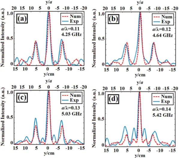
To show the effectiveness of the designed PC lens as a subwavelength focusing device within a wide range of operating frequency, we also performed experimental steps for the frequency range of 4.25 to 5.42 GHz, which can be presented as normalized frequencies of a/λ = 0.11 to 0.14. Figure 6a,b show the transmitted transverse cross-sectional intensity maps, plotted as a function of the incident wave carrier frequency of numerical and experimental results. Figure 6a shows the subwavelength focusing effect with FWHM values of 0.205λ , 0.200λ , 0.195λ , and 0.190λ at defined normalized frequencies of a/λ = 0.11, 0.12, 0.13, and 0.14, respectively. In Fig. 6b, the map of experimental cross sections shows that frequencies of 4.25, 4.64, 5.03, and 5.42 GHz provided the expected strong focusing effect with subwavelength FWHM values of 0.234λ , 0.230λ , 0.225λ , and 0.210λ , respec-tively. Even though the main features appearing in both cases are similar, there is a discrepancy between them due to the fact that microwave experiment with finite horn antenna apertures was conducted with finite step size (spatial resolution). In addition to that, it is fairly difficult to bring the receiver antenna very close to the end surface of the structure. As a result, we see some deviation between the experimental and numerical results presented in Fig. 6.
When we inspect the transverse intensity profiles of light at the four operating frequencies, we see subwave-length focusing of the beam as summarized in Fig. 7. The numerical and experimental results are consistent with Figure 5. (a) Schematic and photographic view of the experimental setup used to investigate the optimized PC lens (optimized at a/λ = 0.14 normalized frequency) at the microwave region. (b) The measured electric field and its transverse cross-sectional profile at 5.42 GHz with a 0.21λ FWHM value. (c) Plot of experimentally measured and numerically calculated FWHM values depending on focal distances.
each other. Moreover, it is clear from these figures that the focused waves have side lobe levels staying under 50% of the maximum intensity value. This result is also proof of the broadband nature of the designed photonic struc-ture. The subwavelength focusing of light is achieved at more than one frequency.
Figure 6. (a) Numerical and (b) experimental plot of the transverse cross section intensity map at the back focal plane of the PC lens at a distance of x = 2.5 mm from the structure for different operating frequencies ranging from a/λ = 0.11 to 0.14 and 4.25 to 5.42 GHz, respectively.
Figure 7. Transverse cross-sectional intensity profiles of the experimental (solid lines) and FDTD (dashed lines) results taken at (a) 4.25 GHz (a/λ = 0.11), (b) 4.64 GHz (a/λ = 0.12), (c) 5.03 GHz (a/λ = 0.13) and (d) 5.42 GHz (a/λ = 0.14) with FWHM values of 0.234λ (FDTD: 0.205λ), 0.230λ (FDTD: 0.200λ), 0.225λ (FDTD: 0.195λ) and 0.210λ (FDTD: 0.190λ), respectively.
Conclusion
In this paper, we proposed an optimization algorithm known as differential evolution (DE) to design a pho-tonic medium made of lossless dielectric circular elements. The aim was to find a phopho-tonic structure that pro-vides strong focusing of light. The algorithm was integrated into a finite-difference time-domain method, and multi-objectives such as narrow full width at half maximum and low-intensity side lobes were defined in the cost function. To the best of the authors’ knowledge, the optimization algorithm based on DE was utilized for the subwavelength focusing for the first time. FWHM values less than 0.25λ in air with low-intensity side lobes were demonstrated both numerically and experimentally. The subwavelength focusing of light is linked with the interference effect and irregular index gradient. Strong focusing of light may improve the resolution of optical imaging and lithography and increase the data storage capacity of optical media. The proposed DE algorithm can be applied to design other photonic structures for additional light manipulation techniques.
References
1. Hecht, E. Optics. (Addison-Wesley, 2001).
2. Joannopoulos, J. D., Johnson, S. G., Winn, J. N. & Meade, R. D. Photonic crystals: molding the flow of light 2nd ed. (Princeton University Press, 2008).
3. Lončar, M. et al. Waveguiding in planar photonic crystals. Appl. Phys. Lett. 77, 1937 (2000).
4. Akahane, Y., Asano, T., Song, B. & Noda, S. High-Q photonic nanocavity in a two-dimensional photonic crystal. Nature 425, 944–947 (2003).
5. Kurt, H. & Citrin, D. S. Photonic crystals for biochemical sensing in the terahertz region. Appl. Phys. Lett. 87, 041108 (2005). 6. Kurt, H., Colak, E., Cakmak, O., Caglayan, H. & Ozbay, E. The focusing effect of graded index photonic crystals. Appl. Phys. Lett. 93,
171108 (2008).
7. Lončar, M., Yoshie, T., Scherer, A., Gogna, P. & Qiu, Y. Low-threshold photonic crystal laser. Appl. Phys. Lett. 81, 2680 (2002). 8. Noda, S., Chutinan, A. & Imada, M. Trapping and emission of photons by a single defect in a photonic bandgap structure. Nature
407, 608–610 (2000).
9. Turunen, J. & Wyrowski, F. Diffractive optics for industrial and commercial applications. (Wiley-VCH, 1998).
10. Turduev, M., Giden, I. H. & Kurt, H. Design of flat lens-like graded index medium by photonic crystals: exploring both low and high frequency regimes. Opt. Comm. 339, 22–33 (2015).
11. Ishii, S., Kildishev, A. V., Shalaev, V. M., Chen, K. P. & Drachev, V. P. Metal nanoslit lenses with polarization-selective design. Opt.
Lett. 36, 451–453 (2011).
12. Chien, H. T. & Chen, C. C. Focusing of electromagnetic waves by periodic arrays of air holes with gradually varying radii. Opt.
Express 14, 10759–10764 (2006).
13. Sanchis, L., Håkansson, A., López-Zanón, D., Bravo-Abad, J. & Sánchez-Dehesa, J. Integrated optical devices design by genetic algorithm. Appl. Phys. Lett. 84, 4460 (2004).
14. Srituravanich, W. et al. Flying plasmonic lens in the near field for high-speed nanolitography. Nat. Nanotechnol. 3, 733–737 (2008). 15. Schuller, J. A. et al. Plasmonics for extreme light concentration and manipulation. Nature Materials 9, 193–204 (2010).
16. Gramotnev, D. K. & Bozhevolnyi, S. I. Plasmonics beyond the diffraction limit. Nature Photon. 4, 83–91 (2010). 17. Grier, D. G. A revolution in optical manipulation. Nature 424, 810–816 (2003).
18. Yang, A. H. J. et al. Optical manipulation of nanoparticles and biomolecules in sub-wavelength slot waveguides. Nature 457, 71–75 (2009).
19. Righini, M., Zelenina, A. S., Girard, C. & Quidant, R. Parallel and selective trapping in a patterned plasmonic landscape. Nature
Phys. 3, 477–480 (2007).
20. Grigorenko, A. N., Roberts, N. W., Dickinson, M. R. & Zhang, Y. Nanometric optical tweezers based on nanostructured substrates.
Nature Photon. 2, 365–370 (2008).
21. Gramotnev, D. K. & Bozhevolyni, S. I. Nanofocusing of electromagnetic radiation. Nature Photon. 8, 13–22 (2014).
22. Jin, Y. & He, S. Canalization for subwavelength focusing by a slab of dielectric photonic crystal. Phys. Rev. B. 75, 195126 (2007). 23. Thongrattanasiri, S. & Podolskiy, V. A. Hypergratings nanophotonics in planar anisotropic metamaterials. Opt. Lett. 34, 890–892
(2009).
24. Ren, G. et al. Subwavelength focusing of light in the planar anisotropic metamaterials with zone plates. Opt. Express. 18, 18151–18157 (2010).
25. Ren, G., Wang, C., Zhao, Z., Tao, X. & Luo, X. Off-axis characteristic of subwavelength focusing in anisotropic metamaterials. J. Opt.
Soc. Am. B 29, 3103–3108 (2012).
26. Ma, C. & Lu Z. A super resolution metalens with phase compensation mechanism. Appl. Phys. Lett. 96, 183103 (2010).
27. Jacob, Z., Alekseyev, L. V. & Narimanov, E. Optical hyperlens: far-field imaging beyond the diffraction limit. Opt. Express 14, 8247–8256 (2006).
28. Marqués-Hueso, J., Sanchis, L., Cluzel, B., De Fornel, F. & Martínez-Pastor, J. P. Genetic algorithm designed silicon integrated photonic lens operating at 1550 nm. Appl. Phys. Lett. 95, 071115 (2010).
29. Hakansson, A. & Sánchez-Dehesa, J. Inverse designed photonic crystal de-multiplex waveguide coupler. Opt. Express 13, 5440–5449 (2005).
30. Preble, S., Lipson, M. & Lipson, H. Two-dimensional photonic crystals designed by evolutionary algorithms. Appl. Phys. Lett. 86, 061111 (2005).
31. Gagnon, D., Dumont, J. & Dubé, L. J. Beam shaping using genetically optimized two-dimensional photonic crystals. J. Opt. Soc. Am.
A 29, 2673–2678 (2012).
32. Jensen, J. S. & Sigmund, O. Topology optimization for nano-photonics. Laser Photon. Rev. 5, 308–321 (2011). 33. Sigmund, O. & Hougaard, K. Geometric properties of optimal photonic crystals. Phys. Rev. Lett. 100, 153904 (2008).
34. Jensen, J. S. & Sigmund, O. Systematic design of photonic crystal structures using topology optimization: low-loss waveguide bends.
Appl. Phys. Lett. 84, 2022 (2004).
35. Frandsen, L. H. et al. Topology optimized mode conversion in a photonic waveguide fabricated in silicon-on-insulator material. Opt.
Express 22, 8525–8532 (2014).
36. Kumar, M. S., Menabde, S., Yu, S. & Park, N. Directional emission from photonic crystal waveguide terminations using particle swarm optimization. J. Opt. Soc. Am. B 27, 343–349 (2010).
37. Piggott, A. Y. et al. Inverse design and demonstration of a compact and broadband on-chip wavelength demultiplexer. Nature
Photon. 9, 374–377 (2015).
38. Shen, B., Wang, P., Polson, R. & Menon, R. An integrated-nanophotonics polarization beamsplitter with 2.4 × 2.4 μ m2 footprint.
Nature Photon. 9, 378–382 (2015).
39. Saucer, T. W. & Sih, V. Optimizing nanophotonic cavity designs with the gravitational search algorithm. Opt. Express 21, 20831–20836 (2013).
40. Shen, B., Polson, R. & Menon, R. Integrated digital metamaterials enables ultra-compact optical diodes. Opt. Express 23, 10847–10855 (2015).
(2009).
54. Guo, W. et al. Near-field laser parallel nanofabrication of arbitrary-shaped patterns. Appl. Phys. Lett. 90, 243101 (2007).
55. Wang, Z. B. et al. Optical near-field distribution in an asymmetrically illuminated tip-sample system for laser/STM nanopatterning.
Appl. Phys. A 89, 363–368 (2007).
56. Wang, Z. B. et al. Optical virtual imaging at 50 nm lateral resolution with a whitelight nanoscope. Nat. Commun. 2, 218 (2011). 57. Betzig, E., Lewis, A., Harootunian, A., Isaacson, M. & Kratschmer, E. Near Field Scanning Optical Microscopy (NSOM). Biophys. J.
49, 269–279 (1986).
58. Pollock, H. M. & Smith, D. A. Handbook of vibrational spectroscopy, Vol. 2 (eds Chalmers, J. M. & Griffiths, P. R.) 1472–1492 (Wiley, 2006).
Acknowledgements
H.K. acknowledges partial support from the Turkish Academy of Sciences. M.T. gratefully acknowledges the support of the TED University Scientific Research Project with Project No: 15A301. The authors would like to thank H. Caglayan from Abdullah Gul University for fruitful discussions.
Author Contributions
E.B., M.T. and H.K. contributed to the discussions, concept development, and analysis of the numerical and experimental results, data processing, writing and reviewing of the manuscript.
Additional Information
Competing financial interests: The authors declare no competing financial interests.
How to cite this article: Bor, E. et al. Differential evolution algorithm based photonic structure design: numerical and experimental verification of subwavelength λ/5 focusing of light. Sci. Rep. 6, 30871; doi: 10.1038/ srep30871 (2016).
This work is licensed under a Creative Commons Attribution 4.0 International License. The images or other third party material in this article are included in the article’s Creative Commons license, unless indicated otherwise in the credit line; if the material is not included under the Creative Commons license, users will need to obtain permission from the license holder to reproduce the material. To view a copy of this license, visit http://creativecommons.org/licenses/by/4.0/