SCANNING HALL PROBE MICROSCOPY (SHPM)
USING QUARTZ CRYSTAL AFM FEEDBACK
A THESIS
SUBMITTED TO DEPARTMENT OF PHYSICS AND THE INSTITUTE OF ENGINEERING AND SCIENCE
OF BILKENT UNIVERSITY
IN PARTIAL FULFILLMENT OF THE REQUIREMENTS FOR THE DEGREE OF
MASTER OF SCIENCE
By Koray Ürkmen September, 2005
ii
I certify that I have read this thesis and that in my opinion it is fully adequate, in scope and in quality, as a thesis for the degree of Master of Science.
___________________________________ Assoc. Prof. Dr. Ahmet Oral (Supervisor)
I certify that I have read this thesis and that in my opinion it is fully adequate, in scope and in quality, as a thesis for the degree of Master of Science.
____________________________________ Prof. Dr. Alexander Stanislaw Shumovsky
I certify that I have read this thesis and that in my opinion it is fully adequate, in scope and in quality, as a thesis for the degree of Master of Science.
______________________________________ Dr. Tarık Reyhan
Approved for the Institute of Engineering and Science:
______________________________________ Prof. Dr. Mehmet Baray
iii
ABSTRACT
SCANNING HALL PROBE MICROSCOPY (SHPM)
USING QUARTZ CRYSTAL AFM FEEDBACK
Koray Ürkmen M.S. in Physics
Supervisor: Assoc. Prof. Dr. Ahmet Oral September, 2005
Scanning Hall Probe Microscopy (SHPM) is a quantitative and non-invasive technique for imaging localized surface magnetic field fluctuations such as ferromagnetic domains with high spatial and magnetic field resolution of ~50nm & 7mG/ Hz at room temperature. In the SHPM technique, Scanning Tunneling Microscope (STM) or Atomic Force Microscope (AFM) feedback is usually used for bringing the Hall sensor into close proximity of the sample. In the latter, the Hall probe has to be integrated with an AFM cantilever in a complicated microfabrication process. In this work, we have eliminated the difficult cantilever-Hall probe integration process; a cantilever-Hall sensor is simply glued at the end of Quartz crystals, which are used as a force sensor. The sensor assembly is dithered at the resonance frequency and the quartz force sensor output is detected with a Lock-in and PLL system. SHPM electronics is modified to detect AFM topography and the phase, along with the magnetic field image. NIST MIRS (Magnetic Referance Sample) (Hard Disk) sample, 100 MB high capacity zip disk and Garnet sample are imaged with the Quartz Crystal AFM feedback and the performance is found to be comparable with the SHPM using STM feedback. Quartz Crystal AFM feedback offers a very simple sensor fabrication and operation in SHPM. This method eliminates the necessity of conducting samples for SHPM.
Keywords: Scanning Tunneling microscopy, Atomic Force Microscopy, Scanning
iv
ÖZET
KUARS KRİSTALİ KULLANILARAK AKM GERİ
BESLEMELİ TARAMALI HALL AYGITI
MİKROSKOPİSİ
Koray Ürkmen Fizik Yüksek Lisans
Tez Yöneticisi: Doç. Dr. Ahmet Oral Eylül, 2005
Taramalı Hall Aygıtı Mikroskopisi (THAM), ferromanyetik malzemelerdeki manyetik alanlar gibi lokalize yüzey manyetik alanlarını yüksek uzaysal çözünürlükle (~50nm ) ve oda sıcaklığında bile 7mG/ Hz manyetik alan çözünürlüğü ile etkileşimsiz ve nicel olarak ölçmek için kullanılan bir tekniktir. THAM tekniğinde, Hall aygıtını yüzeye yaklaştırmak için genellikle Taramalı Tünelleme Mikroskobu (TTM) veya Atomik Kuvvet Mikroskobu (AKM) geribeslemesi kullanılır. AKM geribeslemesi için Hall aygıtının karmaşık bir mikrofabrikasyon yöntemi kullanılarak AKM yayı ile entegre edilmesi gerekir. Bu çalışmada zor olan yay-Hall aygıtı entegrasyonunu gereksiz hale getirdik. Hall aygıtını kuvvet algılayıcısı olarak kullanılan bir kuvars kristali üzerine yapıştırdık. Algılayıcı rezonans frekansında titreştirildi, ve kuvars kristalinin çıktısı Lock in veya PLL sistemleri ile incelendi. THAM elektroniği AKM topografyasını ve faz değişimini manyetik alan bilgisiyle beraber alabilecek biçimde değiştirildi. NIST MIRS (Sabit Disk), 100 MB yüksek kapasiteli ZIP diski ve Demir-Garnet örnekleri Kuvars Kristali AKM geri beslemesi ile görüntülendi ve performansı TTM geri beslemesi kullanılan THAM ile karşılaştıralabilir bulundu. Kuvars Kristalli AKM geribeslemesi THAM için çok basit algılayıcı üretimini ve kullanımını vaad etmektedir. Bu metod THAM uygulaması için örneklerin iletken olması gereksinimini ortadan kaldırmaktadır.
Anahtar sözcükler: Taramalı Tünelleme Mikroskopisi, Atomik Kuvvet
Mikroskopisi, Taramalı Hall Aygıtı Mikroskopisi, Temassız AKM, Kuvars Kristali Çatalları.
v
Acknowledgement
I would like to express my deep gratitude to my supervisor Assoc. Prof. Dr. Ahmet Oral, for his invaluable help and guidance.
I also want to thank to Mehrdad Atabak, Münir Dede, Muharrem Demir, Sevil Özer, Göksel Durkaya, Özgür Güngör, Ayşegul Erol, and especially Özge Girişen for their valuable help, useful remarks and for cheering me up. When I needed help, they were always there for me.
I dept special thanks to Assoc. Prof. Dr. Ceyhun Bulutay, Assoc. Prof. Dr. Lütfi Özyüzer for their friendly attitudes, remarkable help and motivation.
I also would like to express my special thanks to my parents Tacettin and Münevver Ürkmen, my second family Kutay, Bahar and Zeynep Ürkmen, all my brothers, my friends Emre Koçana, Tamer Başer, and Özlem Balkan enhancing my life. They never allowed me to become lonely in my life or during my work.
vi
CONTENTS
1 Introduction ··· 1
1.1 Scanning Tunneling Microscopy (STM) ··· 2
1.2 Atomic Force Microscopy (AFM)··· 5
1.3 Scanning Hall Probe Microscopy (SHPM)··· 12
1.4 Scanning Probe Microscopy (SPM) scanning technique ··· 17
2 Experimental Set-up··· 23
3 SHPM Probe Fabrication ··· 29
4 Scanning Hall Probe Microscopy (SHPM) experiments with STM feedback ··· 39
5 Quartz Tuning fork as a force sensor ··· 46
5.1 Force detection techniques ··· 49
5.1.1 Lock-in Amplifier··· 51
5.1.2 PLL··· 53
5.2 Historical background of the experimental set-up ··· 56
5.2.1 Preparation for High magnetic fields ··· 56
5.2.2 Different diameters for AFM tips ··· 58
vii
5.2.4 Different dither voltages for AFM tips ··· 63
5.2.5 Images at different temperatures··· 67
6 SHPM with AFM feed-back ··· 69
6.1 Lift-off mode SHPM imaging with AFM feed-back··· 89
6.2 Tracking mode SHPM imaging with AFM feed-back ··· 93
7 Conclusion··· 101
viii
List of Figures
Figure 1.1: Schematic view of a dimensional tunneling barrier··· 3
Figure 1.2: Schematic picture of the tunneling geometry. ··· 4
Figure 1.3: Interatomic force vs distance··· 6
Figure 1.4: The basic AFM set-up with beam deflection method. ··· 8
Figure 1.5: AFM cantilevers··· 8
Figure 1.6: A basic 4 quadrant photo detector for beam-deflected AFM set-up. ·· 9
Figure 1.7: Schematic SHPM scan mechanism ··· 13
Figure 1.8: Hall Probe with 50nm effective area ··· 13
Figure 1.9: Schematic description of Hall Effect··· 14
Figure 1.10: Schematic diagram of SPM ··· 17
Figure 1.11. Schematic view of scanner tube ··· 20
Figure 1.12: Sharpness dependent resolution ··· 21
Figure 1.13: Electrochemical etch setup for AFM applications ··· 21
Figure 1.14: SEM image of electrochemically etched W wire. The gray points on the tip are the carbon atoms which are deposited by the graphite electrode. (K.Urkmen and L.Ozyuzer, Izmir Institute of Technology, 2002)··· 22
Figure 1.15: STM image with 8µm x 8µm scan area on 6µm period grating sample at 4.2K, as an example of shadow effect of dual tip. ··· 22
Figure 2.1: Low Temperature Scanning Hall Probe Microscope. ··· 23
Figure 2.2: Low Temperature Scanning Hall Probe Microscope in details.··· 24
Figure 2.3: Slider part contents and the scanner head of LT-SHPM system. ··· 25
ix
Figure 2.5: Available SPM probes: a) STM holder, b) Quartz Tuning Fork AFM
probe, c) SHPM probe.··· 27
Figure 2.6: Our homemade cryostat system which is directly inserted to the liquid nitrogen tank. ··· 28
Figure 3.1: Pseudomorphic High Electron Mobility Transistor P-HEMT wafer and its specifications that is used for Hall Probe fabrication ··· 29
Figure 3.2: Hall Probe with integrated STM tip ··· 30
Figure 3.3: Photolithography process ··· 31
Figure 3.4: Difference of negative and positive resists ··· 31
Figure 3.5: Etch process after photolithography ··· 32
Figure 3.6: Hall Probe definition with photoresist coating, after develop··· 33
Figure 3.7: Hall Probe definition after RIE etch ··· 34
Figure 3.8: Mesa Etch by RIE ··· 35
Figure 3.9: Recess Etch by HCl··· 35
Figure 3.10: Metallization development. ··· 37
Figure 3.11: Doped Au layer after RTP process on Hall Probe contacts ··· 37
Figure 3.12: Finished Hall Probe without STM Tip. ··· 38
Figure 3.13: B-H curves of Hall probes that are fabricated during this thesis work. ··· 38
Figure 4.1: Hall Probe with STM Tip.··· 39
Figure 4.2: Alignment angle for SHPM operation. ··· 40
Figure 4.3: Schematic of alignment mechanism. ··· 41
Figure 4.4: Images of the hall probe and its reflection from the sample surface: a) from the first side after get parallel to the surface, b) from the second side after get parallel to the surface, c) after the tilt angle is given.··· 41
Figure 4.5: Schematic SHPM scan mechanism ··· 42
Figure 4.6: Room temperature SHPM images of NIST magnetic reference sample over 40µm x 40µm area with 128 x 128 pixels resolution, 100 µm/sec scan speed, Lift Off Voltage=2.5V,Hall current= 3 µA, ··· 42
x
Figure 4.7: Room temperature SHPM image of NIST magnetic reference sample
over 40µm x 40µm area with 128 x 128 pixels resolution, 100 µm/sec scan speed, Lift Off Voltage=2.5V,Hall current= 3 µA, (Image shows unprocessed average of
10 fast scan SHPM images)··· 43
Figure 4.8: Low temperature (77K) SHPM image of Zip magnetic storage sample over ~17.6 µm x 17.6 µm area with 256 x 256 pixels resolution, 100 µm/sec scan speed, Lift Off Voltage=5V ( 0.43 µm ), Hall current= 20 µA, (Image shows unprocessed average of 4 fast scan SHPM images ··· 44
Figure 4.9: Room Temperature tracking mode image of Iron-Garnet sample over 54µm x 54µm scan area, with 2 µm/sec scan speed, 2 µA Hall current and RH = 0.1960 Ohm/Gauss Hall coefficient [16]··· 45
Figure 5.1: Resonance curve of 32 kHz Quartz Tuning Fork crystal in its own shield, calculated Q-factor is 102,710 ··· 47
Figure 5.2: 32 kHz Quartz tuning forks sizes, where each small interval is 1/100 inches. ··· 47
Figure 5.3: 100 kHz Quartz tuning fork sizes, where each small interval is 1/100 inches. ··· 48
Figure 5.4: 32 kHz Quartz tuning fork without original shield. ··· 48
Figure 5.5: Resonance and phase curve of a tip attached quartz tuning fork. ··· 50
Figure 5.6: Resonance and phase shift of quartz crystal with applied force.··· 50
Figure 5.7: The connection scheme of the lock-in and SPM electronic system ·· 52
Figure 5.8: AFM image of 6µm period grating at room temperature with lock-in amplifier, over 52 µm x 52 µm area with 1 µm/s speed··· 52
Figure 5.9: AFM image of 6µm period grating at low temperature with lock-in amplifier, over 8 µm x 8 µm area with 1 µm/s speed··· 52
Figure 5.10: Quartz AFM image of Morexalla bacteria over 2µm x 3µm area with 1µm/s speed, by using lock-in amplifier··· 53
Figure 5.11: The connection scheme of the PLL and SPM electronic system ···· 53
Figure 5.12:PLL circuit design ··· 54
xi
Figure 5.14: The connections of the PLL card with feedback circuit and spare
ADC circuit··· 55
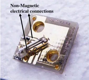
Figure 5.15: Old type of AFM probe with magnetic materials. ··· 56 Figure 5.16: New type of AFM probe with non-magnetic electrical connections57 Figure 5.17: AFM image of 6 µm period grating, taken at 10 K, under 3.5 Tesla
magnetic field with the new type quartz tuning fork AFM probe by using lock-in system and Quantum Design’s PPMS system. ··· 57
Figure 5.18: AFM image of 6 µm period grating, taken at 10 K, under 7 Tesla
magnetic field with the new type quartz tuning fork AFM probe by using lock-in and Quantum Design’s PPMS system. ··· 57
Figure 5.19: Old type of AFM probe with 125 µm thick etched Tungsten tip ···· 58 Figure 5.20: New type of AFM probe with 50 µm thick etched Tungsten tip··· 58 Figure 5.21: Old type of AFM probe with 0,125 mm tungsten tip, 0.5 Vrms dither
voltage, 29,360 Hz Resonance Frequency and 326 Q-Factor ··· 59
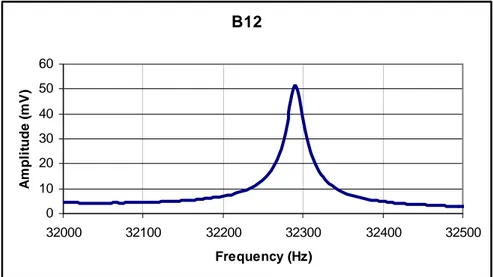
Figure 5.22: New type of AFM probe with 0.5 Vrms dither voltage, 32,290 Hz
Resonance Frequency and 6,458 Q-Factor ··· 59
Figure 5.23: Error signal (force gradient) image of 3µm period grating with
125µm diameter Tungsten wire obtained using PLL ··· 60
Figure 5.24: Phase shift signal image of 3µm period grating with 125µm diameter
Tungsten wire obtained using PLL··· 60
Figure 5.25: Feed-back signal image of 3µm period grating with 125µm diameter
Tungsten wire obtained using PLL··· 60
Figure 5.26: Cross section of feedback image of 3µm period grating with 125µm
diameter Tungsten tip··· 61
Figure 5.27: Error signal (force gradient) image of 6µm period grating with 50µm
diameter Tungsten tip, by using PLL system··· 61
Figure 5.28: Phase shift signal image of 6µm period grating with 50µm diameter
Tungsten tip, by using PLL system ··· 61
Figure 5.29: Feed-back signal image of 6µm period grating with 50µm diameter
xii
Figure 5.30: Cross section of feedback image of 6µm period grating with 50µm
Tungsten tip ··· 62
Figure 5.31: Resonance frequency change with temperature··· 63 Figure 5.32: Q-factor change with temperature ··· 63 Figure 5.33: AFM imaging with 40 mV RMS dither amplitude, 4µm/s scan speed,
100µs Lock-in time constant ··· 64
Figure 5.34: AFM imaging with 4 mV RMS dither amplitude, 3.5µm/s scan
speed, 100µs Lock-in time constant, ··· 65
Figure 5.35: AFM imaging with 2 mV RMS dither amplitude, 3.5µm/s scan
speed, 100µs Lock-in time constant, ··· 65
Figure 5.36: AFM imaging with 1 mV RMS dither amplitude, 3.5µm/s scan
speed, 100µs Lock-in time constant, ··· 66
Figure 5.37: AFM imaging with 0.5 mV RMS dither amplitude, 3.5µm/s scan
speed, 100µs Lock-in time constant ··· 66
Figure 5.38: AFM feedback data at 300K, over 21 µm x 21 µm area with 128 x
128 pixels resolution and 1 µm/sec speed. Image shows a 6 µm x 6 µm square periodic arrays with 4 µm squares and 2 µm spacing (Processed images) taken with Lock-in.··· 67
Figure 5.39: AFM feedback data at 4.2K, over ~17.6 µm x 17.6 µm area with 256
x 256 pixels resolution and 0.15 µm/sec speed. Image shows a 6 µm x 6 µm square periodic arrays with 4 µm squares and 2 µm spacing (Processed images) taken with Lock-in. ··· 68
Figure 6.1: Microfabricated piezoresistive SHPM combined AFM cantilevers,
[27, 28]··· 70
Figure 6.2: Microfabricated piezoresistive SHPM combined AFM cantilevers,
[27, 28]··· 70
Figure 6.3: Fabrication process schematic SHPM integrated AFM cantilevers.
[27, 28]··· 71
Figure 6.4: Piezoelectric feedback mechanism for SHPM with two piezo plates
xiii
Figure 6.5: Quartz Tuning Fork AFM guided Scanning Hall Probe ··· 72 Figure 6.6: Forward of 6µm period grating with the corner of a dummy Hall
Probe chip ··· 73
Figure 6.7: Quartz Tuning Fork AFM guided Scanning Hall Probe ··· 74 Figure 6.8: Quartz Tuning Fork AFM guided Scanning Hall Probe with two free
prongs ··· 75
Figure 6.9: Getting glued one of the prongs of the quartz tuning fork to avoid the
broken symmetry problem.··· 75
Figure 6.10: Quartz tuning fork, prong and crystal sizes ··· 79 Figure 6.11: Measured resonance curve for a full Hall Probe attached 100 kHz
quartz tuning fork between 5,000 Hz and 35,000 Hz ··· 80
Figure 6.12: Measured resonance curve for a full Hall Probe attached 100 kHz
quartz tuning fork between 35,000 Hz and 70,000 Hz··· 80
Figure 6.13: Measured resonance curve for a full Hall Probe attached 100 kHz
quartz tuning fork between 9,000 Hz and 13,000 Hz with fixed prong. ··· 81
Figure 6.14: Resonance curve of the quartz tuning fork with ¼ sized Hall probe.
··· 82
Figure 6.15: AFM topography by using the corner of the dummy chip ··· 82 Figure 6.16: Photographs of Hall Probe definition and mesa corner of the used
dummy Hall Probe for the feed-back tracking experiment ··· 83
Figure 6.17: Resonance tune between 5,000 and 100,000 Hz of 100 kHz Quartz
crystal with dummy Hall Probe··· 84
Figure 6.18: Resonance and the phase curve of 100 kHz Quartz crystal with
dummy Hall Probe that is used for experiment··· 84
Figure 6.19: Results of AFM topography imaging by using corner of Mesa (1)
over 20µm x 20µm area with ∆ƒ =15 Hz, 1µm/s ··· 85
Figure 6.20: Results of AFM topography imaging by using corner of Mesa (2)
over 15µm x 15µm area with ∆ƒ=8 Hz, 1µm/s ··· 86
Figure 6.21: Results of AFM topography imaging by using corner of Mesa (1)
xiv
Figure 6.22: Results of AFM topography imaging by using Mesa corner (3), over
20µm x 20µm area with ∆ƒ =25 Hz, 2µm/s ··· 88
Figure 6.23: Vacuuming pump for both insert shield and cryostat. ··· 89 Figure 6.24: SHPM image of the data tracks on the 100 MB ZIP media obtained
in the lift-off mode ··· 90
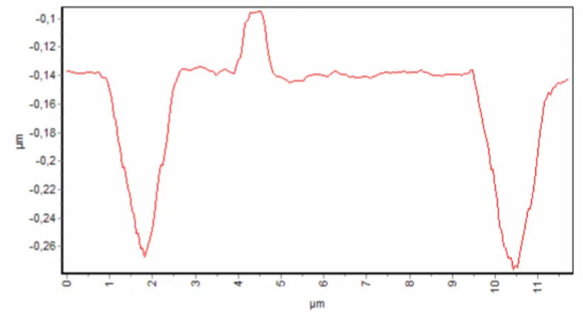
Figure 6.25: Cross section of the data tracks ··· 90 Figure 6.26: SHPM image with Quartz AFM feedback, at 77K by using 5V
lift-off voltage ··· 91
Figure 6.27: Cross section path on image and graph of cross section of the data
tracks··· 91
Figure 6.28: Cross section path on image and graph of cross section of the data
tracks in Gauss scale ··· 93
Figure 6.29: Resonance curve of the Hall Probe attached quartz tuning fork, at
300K. ··· 94
Figure 6.30: Tracking mode SHPM image with Quartz AFM feedback, at 300K.
··· 94
Figure 6.31: Cross section path on image and graph of cross section of domains
··· 95
Figure 6.32: Resonance curve of the Hall Probe attached to quartz tuning fork, at
300K. ··· 95
Figure 6.33: Quartz AFM feedback tracking mode, force, phase and feedback
data at 77K. ··· 96
Figure 6.34: Quartz AFM feedback tracking mode SHPM image at 77K.··· 96 Figure 6.35: Cross section path on image and graph of cross section of domains
··· 96
Figure 6.36: Quartz AFM feedback tracking mode, force, and phase and feedback
images at 77K.··· 97
Figure 6.37: Tracking mode SHPM image with Q-AFM feedback, at 77K (2). · 97 Figure 6.38: Filtered and enhanced color tracking mode SHPM image with
xv
Figure 6.39: Cross section path on image and graph of cross section of the
domains (2) ··· 98
Figure 6.40: Quartz AFM feedback tracking mode, force, phase and feedback
data at 77K. ··· 99
Figure 6.41: Tracking mode SHPM image with Quartz AFM feedback, at 77K.(3)
··· 99
Figure 6.42: Cross section path on image and graph of cross section along the
xvi
List of Tables
Table 6-1: Sizes of one prong of 32 kHz quartz tuning fork and density of quartz ··· 76 Table 6-2: Sizes and density of Hall probe ··· 76 Table 6-3: Sizes of one prong of 100 kHz quartz tuning fork and density of quartz ··· 78 Table 6-4: Prong sizes, spring constants and calculated resonance frequencies of
1
Chapter 1
Introduction
Perhaps the most important ability of the humanity is developing tools and using them in the daily life. Although human beings are not strong enough to survive in nature, the tough we are one of the strongest creatures by using these tools. This ability can also be named as intelligence. Nowadays, the tools are still being developed to achieve a more comfortable and easier life for humanity. Nanotechnology and especially nanotechnology related tools are very important to achieve more functionality in gadgets for this purpose.
Humanity had to have a chance to investigate and understand a new world at atomic scales with the invention of the Scanning Tunneling Microscope (STM) by Gerd Bining and Heinrich Rohrer, at IBM laboratories, in 1981. This invention, which effectively started the nanotechnology, brought a Nobel Prize in physics to its inventors in 1986. With this invention, the researches focused on nanotechnology and new imaging techniques at nano-scale. In 1985, the invention of Atomic Force Microscopy (AFM) followed the STM. These new Scanning ProbeMicroscopy (SPM) techniques, as AFM, increased measurement ability and enlarge the knowledge at this nano-scale with wider range of sample types and surface properties. With increasing interest to these systems, it is succeed to made
atom manipulation and nano-lithography. These developments also allowed scientists to fabricate nano-scale mechanical and electronic devices. In their first applications, SPMs were used mainly for measuring 3D surface topography. Although 3D surface topography is still their primary application, they can now be used to measure many other surface properties as surface magnetic or electrical properties.
Magnetic imaging with Scanning Hall Probe Microscopy (SHPM) provides quantitative and non-invasive magnetic measurements at nanometer scale. SHPM technique is very important way of the understanding magnetic properties and magnetic behavior of magnetic and superconducting materials. In this thesis two of these tools AFM and SHPM are combined to a new, simple and cheaper solution to magnetic imaging of non-conducting materials. I will first describe the theory of STM. Then the thesis will continue with the theory of AFM and SHPM. Then a brief summary of superconductivity will be given. Experimental set-up and its history will be described. At the end with the results, conclusion and the future work will be summarized.
1.1 Scanning Tunneling Microscopy (STM)
One of the best known difference between classical and quantum mechanic is the quantum tunneling phenomena. In classical mechanics, if a ball is thrown into a wall, there is no doubt to be reflected back. But in quantum mechanics, there is a probability of tunneling of the ball, depending on the wall thickness and its kinetic energy. So according to the quantum mechanics an electron can penetrate through a potential barrier. In this forbidden region the wave function, ψ, of the electron decays exponentially. [1]
h z E m z) (0)exp 2 ( ) ( =ψ − φ− ψ (1.1)
Where m is the mass of the particle (electron) and =1.05×10⁻³⁴
h Js.
Figure 1.1: Schematic view of a dimensional tunneling barrier
This is a very simple theory to explain the tunneling phenomena. The most successful theory was developed by Tersoff and Hamann in 1983. Tersoff and Hamann modeled the tip as a spherical potential well, as illustrated in Figure 1.2 [2]. Here R is the local radius of curvature of the tip and d is the distance of the nearest approach to the surface.
By using the first order perturbation theory, the tunneling current can be written as, ) ( ) ( 1 )[ ( ) / 2 ( π µν f Eµ f Eν eV Mµν 2δ Eµ Eν I = h
∑
− + × − (1.2)Here, f (E) is the Fermi function, V is the bias voltage, Mµν is the tunneling
matrix element between states ψµ of the probe and ψν of the surface, and E is µ
the energy of state ψµ in the absence of tunneling. For the small voltages and temperatures, the equation takes the following form,
Figure 1.2: Schematic picture of the tunneling geometry. ) ( ) ( ) / 2 ( 2 2 F F E E E E M V e I = π h
∑
µν µν δ ν − δ µ − (1.3)where EF is the Fermi level. Here the main problem is the calculation of the
tunneling matrix. Bardeen [3] was found a solution for this as,
) ( ) 2 / ( 2 ⋅ ∗∇ − ∇ ∗ =
∫
µ ν ν µ µν m dS ψ ψ ψ ψ M h (1.4)To evaluate theMµν, Tersoff and Hamann expand the surface wave function µ
ψ and tip wave function
ψ
ν into Bloch states. Finally, one can calculate the tunneling matrix with this method as;) ( Re 4 ) 2 / ( 2 1 1/2 0 → − −Ω = m k k r Mµν h π t kRψν (1.5)
where Ω is the probe volume,t
2 / 1 1(2 )− − = mϕ
k h ,ϕ is the work function and 0 →
r
is the center of curvature of the tip. So tunneling current can be expressed as, Tip
) ( ) ( ) ( 32 2 0 2 4 2 2 2 1 3 F kR F t E R k e r E E D V e I = ×
∑
− → − − ν ν ν δ ψ ϕ π h (1.6)where Dt(EF) is density of states at the Fermi level at the tip. Finally the tunneling can be found as, [4]
) , ( 0 F t r E → ∝ρ σ (1.7) where, ) ( ) ( ) , ( 2 0 E r E E r F =
∑
Ψ − → → ν ν ν δ ρ (1.6)is the local density of the states at position →r and the energy E, for the surface.
Then it can be said that if the tip is not modified during the experiment and the distance is large enough, the STM data corresponds by charge density corrugation on the sample. The theory is only valid for the small s distances.
1.2 Atomic Force Microscopy (AFM)
In 1986, during the STM experiments it was seen that the barrier height between the tip and the surface dropped to zero at small separations. Coombs and Pethica [5] suggested that this small barrier height was caused by the repulsive force interaction between the tip and the sample. With this prediction the AFM was introduced by Binnig, Quate and Gerber. In this method, the force interaction between a sharp tip and the surface is measured with the help of a sensitive force detector, instead of tunneling current and utilized to scan the surface at a constant
height. Because this technique does not depend to the tunneling current during the experiment, it also provides the imaging of the non-conducting samples. This capability brings Scanning Probe Microscopy (SPM) technique to work in a wider sample range. This can be taken as the main advantage of the AFM.
The atomic forces near by the surface can be divided two parts as the long range van der Waals forces and short range chemical forces. Short range chemical forces arise from the overlap of electron wave functions and from the repulsion of the ion cores. Therefore, the range of these forces is comparable to the extension of the electron wave functions, less than one nanometer [1].
The short range forces can be modeled with the Morse potential. The Morse potential describes (1.7) a chemical bond with bonding energyEbond, equilibrium
distanceσ , and a decay lengthκ. While the Morse potential can be used for a qualitative description of chemical forces, it lacks an important property of chemical bonds: anisotropy. Another model used widely is the Lennard-Jones potential (1.8). [6]
) 2 ( −κ(−σ)− −2κ(−σ) − = z z bond Morse E e e V (1.7) ⎟⎟ ⎠ ⎞ ⎜⎜ ⎝ ⎛ − − = − 12 12 6 6 2 σ σ z z E
VLennard Jones bond (1.8)
On the other hand, van der Waals forces are dipole-dipole forces. They are caused by the fluctuations in the electric dipole moment of atoms and their mutual polarization. They always exist and they are always attractive. In short ranges van der Waals forces decays as 1 r/ 7
F ∝ , where as beyond r ≈ 5nm this power
reduces to 1 r/ 8
F ∝ [1]. There are two ways for calculating van der Waals forces.
In first one the molecular forces are summed up for each geometry with assuming that they are pair wise additive. But the best way to calculate them is the Lifshitz theory. [1]
For the AFM experiments, force interaction between the surface and the tip can be measured by using tunneling detection, capacitance detection [7], beam deflection method [8] and piezoresistive measurement [9], piezoelectric [17] and interferometer [30].
In the first AFM, tunneling detection method is used to measure the cantilever deflection. STM tip is simply positioned behind the AFM cantilever and the change at the tunneling is measured between the STM tip and the back surface of the AFM cantilever. Although this method seems very sensitive for the force measurement, there are several problems as thermal drift and the surface roughness of the cantilever.
In the capacitive detection of the AFM, the back side of the cantilever is used simply as one of the electrode of a capacitor. An electrode is located at the back side of the cantilever as the second electrode of the capacitor. The air barrier between these two electrodes acts as dielectric. The capacitance change between
the AFM cantilever and the fixed electrode is observed to see the changes in applied force. With the capacitance change, feed-back circuit can track the force change easily.
The most common method for the force measurement in AFMs is the optical beam deflection method. In this method, the backside of the cantilever is used as a mirror for a laser beam (Figure 1.6). A laser beam is focused onto the cantilever and deflected beam is collected at a quadrant photo detector. The schematic of a 4 quadrant photo detector is given in Figure 1.7.
Figure 1.4: The basic AFM set-up with beam deflection method.
With the help of a micro-positioner or piezo drivers the optical beam is located at the middle of the detector. The applied force causes the angle change at the deflection of the optical beam. With this angle change, the optical beam is shifted and of the optical power incident on the quadrants of the photo detector changes. The corresponded signal is measured by the photo detector. Using OPAMPs, this signal is used as an input for the feed-back loop. The feed-back loop works to recover the input signal to its beginning value by moving the sample up and down. The feed-back mechanism is also examined in the next part of this thesis. Almost all commercial room temperature ambient AFMs are based on this measurement technique. Although it is a very effective technique, limitations and practical design problems occurs for the special condition AFM microscopes as ultra high vacuum and low temperature conditions. The sensitivity of this technique can be as low as 2×10⁻⁴Å
Hz
/ .
Figure 1.6: A basic 4 quadrant photo detector for beam-deflected AFM set-up. Another method for force measurement is the piezoresistive measurement. In this method, the AFM cantilever is fabricated by using piezoresistive materials or the back side of the cantilever can be coated with the piezoresistive materials like Si or GaAlAs [10]. The resistance of the piezoresistive element changes with the applied force to the cantilever. One can measure the tip-sample force measuring the resistance change by using a Wheatstone bridge. This technique does not require optical alignment and extra elements, and therefore it is very effective for low temperature applications, where the working area is limited.
A B
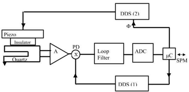
Piezoelectric cantilevers, such as quartz tuning forks, can also be used for force detection. In this method the cantilevers are dithered mechanically at the piezoelectric cantilevers resonance frequency with the help of a dither piezo. Piezoelectric cantilevers generate a voltage proportional to mechanical vibration amplitude. When a force is applied to the cantilever, the generated signal is changed. This change can be measured by comparing the shifted signal with initial resonance frequency. Then the changes are used as inputs for the feed-back mechanism.
AFM can be run basically in three modes: contact mode, non-contact mode and tapping (intermittent contact mode).
In contact mode, short range repulsive chemical forces play a role in measurement. In this mode, tip is gently touching to the surface. In this mode tip and the sample are damaged sligthly during the experiment. In contact mode harder materials are used for tip material as SiO2 or SiN instead of Si tips. In
contact mode, forces that are used to record data are grater than 10-9 N. Ferrante and Smith [11] have calculated the adhesive forces for several metals. According to these, the force of a single atom tip must be reduced to 10-10 N to avoid the deformation of the surface.
In non-contact mode, the cantilever is driven at its resonance frequency with an AC signal with the help of a dither piezo. And the resonance shift is measured by the system. So, in this method the force gradientF'=−∂Fz /∂z is measured
instead of force. In this mode, short range repulsive chemical forces loose their effect. Van der Waals forces, electrostatic forces and magnetic forces can be measured by this method. The effective spring constant of the cantilever in this method can be written as,
'
F k
keff = − (1.9)
Here, k is the spring constant of the cantilever in the absence of tip-surface force interaction. So it can be seen that an attractive force interaction between tip and surface (positive 'F ) soften the effective spring constant and the repulsive
force interaction between tip and surface (negative 'F ) strengthens the effective
spring constant. The change in effective spring constant cause a frequency shift, w. This relationship can be explained as,
2 / 1 0 2 / 1 2 / 1 2 / 1 2 / 1 ' 1 ' 1 ' ⎟ ⎠ ⎞ ⎜ ⎝ ⎛ − = ⎟ ⎠ ⎞ ⎜ ⎝ ⎛ − ⎟ ⎠ ⎞ ⎜ ⎝ ⎛ = ⎟ ⎠ ⎞ ⎜ ⎝ ⎛ − = ⎟⎟ ⎠ ⎞ ⎜⎜ ⎝ ⎛ = k F w k F m k m F k m k w eff (1.10)
Where m is the effective mass and w is the resonance frequency of the 0
cantilever. If F is small relative to k the equation can be re-written as, ' ⎟ ⎠ ⎞ ⎜ ⎝ ⎛ − ≈ k F w w 2 ' 1 0 (1.11) and, k F w w 2 ' 0 − ≈ ∆ (1.12)
So, the attractive force causes a decrease at the resonant frequency where the repulsive force cause increase at resonant frequency. On the other hand the relation between shift in the resonant frequency and the cantilever oscillation A can be written by using the perturbation theory as,
ϕ ϕ π ϕ π cos ) cos ( 2 2 0 0 A z F d kA w w + = ∆
∫
(1.13)Where the integration is over the one oscillation cycle and z is the time averaged position of the tip. To achieve to good resolution in the non-contact force detection, we need a cantilever with soft spring constant, high resonance frequency and high quality factor. High quality factor increase the sensitivity measurement of the system and soft spring constant increase the deflection of the cantilever with force interaction. [12].
1.3 Scanning Hall Probe Microscopy (SHPM)
The surface examination of the materials is not limited only with the surface topography. The magnetic properties of the materials are very important. There are number tools for the magnetic measurement and imaging. Magnetic Force Microscopy (MFM) is the one of the best known magnetic imaging technique. It is a modified AFM technique. It measures magnetic force between magnetized tip and sample. The tip of the cantilever is coated with magnetic materials and magnetized. As the tip is scanned above the surface, magnetic forces acting to the tip deflect the cantilever. Although this is the best known and common magnetic imaging technique with a high spatial resolution, it is invasive and its magnetic field resolution is ill defined. Alternatively Superconducting Quantum Interference Devices’ (SQUID’s) can also be used for the magnetic measurement and magnetic imaging. SQUID’s are known as the most sensitive magnetic flux sensors in the world. Their magnetic field resolutions can be up to 10-16 Tesla and they are also non-invasive measurement systems. But unfortunately their spatial resolution is limited to ~ 1µm and the noise increases while decreasing the effective area of the circuit to have a better spatial resolution. The Scanning Hall Probe Microscopy (SHPM) has a better spatial resolution than SQUID’s and
better magnetic resolution then MFM and non-invasive. The SHPM technique uses the Hall Effect in semiconductors. In SHPM, the properties of Hall Probe material determine the magnetic field resolution where the size of the active area determines the spatial resolution. It is reported that the best achieved spatial resolution is the 50nm with a bismuth Hall probe with an active area of 50nm x 50nm as shown in Figure 1.9 [13].
Figure 1.7: Schematic SHPM scan mechanism
The measurement only takes a place at the small square active area between the arms of the probe. A Hall current is passed between the opposite two arms, and the produced voltage, by the perpendicular magnetic field, is measured.
The Hall Effect is first observed by Edwin Herbert Hall in 1879. When a current flows along a conductor in a magnetic field perpendicular to the direction of the current, a Hall voltage is created across the conductor and perpendicular to the magnetic field and the current. Physically, the magnetic field causes the charge carriers to deviate from their original path and swerve towards the side. The Lorentz force (1.14) causes the deflection of the charge carriers.
→ → → × =q B F υ (1.14)
Figure 1.9: Schematic description of Hall Effect
If the carriers are electrons the forces directions will be as in the Figure 1.10. The Lorentz force Fm
→
and the force Fe
→
which caused by the accumulation of the electrons will cancel each other and an equilibrium is established.
→
B
+ + + + --
--
-
e F → m F → t L wI
VH→ → = e m F F (1.15) → → → = × −q(υd B) qE (1.16) B E =−υd (1.17)
If we assume Q is the total moving charge with the drift velocityυd,
nwtLq
Q= (1.18)
Where n is the free carrier density. Then the transition time to pass through the way L is,
d L υ
τ = (1.19)
And the current that pass through the way L an be found as,
d d twnq L twnLq Q I υ υ τ = = = / (1.20)
If we now re-written the Equation 1.17,
w V wtqn IB E =− = H (1.21)
tqn IB
VH =− (1.22)
And the Hall constant can be found as,
qn
RH =− 1 (1.23)
So if we measure the Hall voltage generated for the applied magnetic fields, we can calculate the Hall coefficient RH. Then, using this Hall coefficient it is
possible to measure the unknown magnetic fields just above the surfaces. For a calculated RH and known magnetic field one can easily calculate the free carrier
density using Equation 1-23. Alternatively, if we know RH, the applied magnetic
field can be measured easily by using the measured Hall voltage by using relation 1.23.
H H
H I GBR
V = (1.24)
1.4 Scanning Probe Microscopy (SPM) scanning
technique
Figure 1.10: Schematic diagram of SPM
Scanning probe microscopy is the general name of the STM, AFM and similar techniques. The scanning mechanism of all the SPM techniques is similar each other. The sensor/tip is brought very close to the surface, using a coarse approach mechanism, and then it is scanned across the surface, acquiring data at each x-y point.
Because of the very fine movements are necessary for the SPM techniques, piezoelectric materials are used for scanners. The scanner range is typically between 1-100 µm in xy and 0.1-10 µm in z direction. In piezoelectric effect, an applied voltage between two electrodes of the material causes a change in stress and strain. By using this effect, a well controlled extension can be provided at the material. The reversible piezoelectric is also available. An applied stress or strain
Feedback Control X-Y Scan Control
Data Acquisition X Y Z Sample Tunneling current ( Iα z/ z0 e− ), Atomic Force, Capacitance, Magnetic force, Adhension, V bias
causes an electric field to develop in the material. The extension that is caused by the applied electric field properties depends on the dimensions and geometry of the material. The resultant displacement coefficient for a PZT tube (2 inch long, 0.5 mm thick, 6.35 mm in diameter) is in a few thousands Å per volt in x-y directions. Therefore with a fine voltage source and with a good choice of piezoelectric material, extensions in Å scale is possible. These properties of piezoelectric materials are used for both coarse approach in z direction and fine scanning on x-y-z plane.
Although the piezoelectric material provides sub-Å scale movements, their maximum extension ranges are limited in µm scale. Therefore another, approach mechanism is needed for the coarse approach. A step motor can be used for this purpose. The important point here, the each step of the stepper should be less than scanner range in z. Otherwise the probe can be crashed to the surface. Generally an automatic approach procedure is established for the coarse approach process. This automatic approach routine first searches the probe-surface interaction is found or not by extending the z piezo. If the interaction (tunnel current, force, etc...) is not found, the sensor/tip is pulled back and a step is made with the coarse positioner. Because the steps of the coarse approach mechanism are smaller than the range of the fine approach there is no chance to crash the probe to the surface. Another example for the coarse approach mechanism is the slip-stick mechanism which is also used in our experimental setup. A metal slider puck is fixed on quartz tube, which is glued to a piezo tube, with the help of a leaf spring. When the quartz tube moves forward slowly and then pulled back suddenly, the slider puck can not overcome its inertia and slides with respect to the quartz tube.
After the coarse approach, the second most important part in SPM is the scanning mechanism. The probe is moved on the surface on a controlled manner with the help of piezoelectric materials which controls the movement in x-y plane. For each x-y-z direction coordinate, the data is recorded during the scan and
stored in a matrix. So the images are 3D in SPM techniques where there is a surface properties measurement data for each x-y coordinate. This surface property data can be height data for STM and AFM techniques or can be a magnetic field strength for SHPM technique. Generally we can talk about two methods for the scanning process. The first one is known as constant height mode. In this mode, the z position of the probe does not change during the scan. Only the change in the interaction (force, tunneling current, magnetic field etc…) is recorded. This technique is simpler and the more dangerous one. If there is a point on the surface, which is higher than the distance between the probe and the surface, the probe can be crashed onto the surface. On the other hand the probe can be too far from the surface, and then the interaction will be lost. To avoid these disadvantages, constant current/interaction mode, can be used. In this mode, the distance between the probe and surface is kept constant with the help of the feedback loop driving piezoelectric scanner. In STM the tunneling current, in AFM the force is kept constant for this purpose. A simple feed-back loop is utilized to achieve this. Feed-back loop moves the sensor towards the sample when the probe current/force is decreased and moves the sensor away if the interaction is increased. So the distance between the probe and surface is kept constant during the scan process. The voltage applied to the z-piezo, is logged as the data for the surface topography. Because the voltage change at piezo is mostly linear with the distance change between the surface and probe, the feedback data is smoother and more reliable from the direct measurement data especially for the STM operation. On the other hand, the scan is done slowly, line by line. Typically, the data are taken for two times, one for forward movement and another one reverse movement. This also provides a verifying mechanism for the reliability of the measurement.
A 4 quadrant scanner piezoelectric tube is usually used for scans in x-y plane and fine movement in z direction. The working mechanism can be explained below.
Figure 1.11. Schematic view of scanner tube
Here, with applying different voltages to the different quadrants of the scanner tube cause different extensions at each quadrant. By using this mechanism the scan process can be supplied as in Figure 1.11. Movement in x-y plane is limited with 56 µm where the length of the scanner piezo is 2 inch. So we can ignore the angle that cased by crimping. If we apply to all quadrants the scanner tube extends or retracts.
It is also possible to extend or retract the tube in the z direction at the same time when scanning it to x and y directions with applying voltages with different values. The z-voltage is simply added to the 4 quadrants using high voltage amplifiers.
Other important parameter for the SPM techniques is the quality. This depends on probe quality and responsible from the resolution in x-y plane. This resolution is named as “spatial” resolution. To increase the spatial resolution the sharpness of the tip for STM and AFM processes and the active area of the probe for SHPM probe are important (Figure 1.12). The common way to get sharper tips to increase the spatial resolution can be given as the electrochemical etching
process. A tungsten wire can be etched with the typical values of 7 V and with a typical 2M NaOH or KOH solution for the AFM tips (Figure 1.13). Because the tungsten wire gets oxidized quickly, the Pt-Ir tips are commonly preferred for the STM operations. The Pt-Ir tips can be also etched electrochemically in NaCl or can be cut for the STM [14,15]. For the micro fabricated device probes as SHPM probes, the size of the effective active area determines the resolution.
Figure 1.12: Sharpness dependent resolution
Figure 1.13: Electrochemical etch setup for AFM applications Image
Scan Area Image
b)
Scan Area
Figure 1.14: SEM image of electrochemically etched W wire. The gray points on the tip are the carbon atoms which are deposited by the graphite electrode.
(K.Urkmen and L.Ozyuzer, Izmir Institute of Technology, 2002)
Figure 1.15: STM image with 8µm x 8µm scan area on 6µm period grating sample at 4.2K, as an example of shadow effect of dual tip.
23
Chapter 2
Experimental Set-up
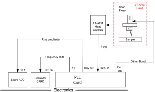
As a main part of our experimental setup we used Nanomagnetics Instruments’ commercial Low Temperature Scanning Hall Probe Microscope (LT-SHPM) system [31]. This LT-SHPM system includes mainly two parts as microscope (Figure 2.1 and 2.2) and SPM control electronics.
Figure 2.2: Low Temperature Scanning Hall Probe Microscope in details. The microscope is composed of the scanner piezo, slider piezo, slider, sample holder and electrical connections. Scanner piezo is used for the scan with resolution in Å scale and fine approach. Probe head fixes the probe with the help of 2 screws and provides the electrical connections of the Hall probe and STM tip. Slider piezo is used for the coarse approach and coarse x-y movement. The scan range of the scanner piezo tube of our system is ~ 56µm x 56µm on the x-y plane and the extension range is ~ 4.8 µm at room temperature. The piezo constants change with the temperature. Piezo constants decrease by factor of 3.8 when the system is cooled from room temperature to 77K.
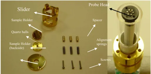
In LT-SHPM system, the probe is simply screwed to the probe head which is just located on the scanner piezo (Figure 2.3). The sample is fixed to the sample holder with silver paint to carry bias voltage to the sample. Front and back sides of the sample holders are screwed to each other. Screw does not fix the sample holder to the slider. A spring is located on screws to fix the sample holder to the slider part. This provides coarse moving of sample on the slider puck. High
Probe head Scanner Piezo tube Slider Piezo tube Probe Slider Quartz tube
voltage pulses applied to the appropriate electrodes of slider piezo to extend it on x-y directions to provide this coarse movement of sample holder. The quartz balls that are located between the sample holder parts and slider puck make this x-y movement with less friction. The slider puck can be fixed to the main part of the slider with using spacers for normal AFM and STM operations. In AFM and STM operations, angle between the probe and the sample is not critical. For SHPM operations the angle between the probe and sample plays an important role. Because of this, slider puck is fixed with alignment springs as shown in Figure 2.3.
Figure 2.3: Slider part contents and the scanner head of LT-SHPM system. After the slider part get ready, the slider is fixed on the quartz tube of the microscope with the help of a leaf spring. It can move with a powerful pulse with using stick-slip movement. The bias voltage cable is connected to the related part of the slider. The movement of the slider part is controlled firstly by hand and then by sending high voltage pulses to the slider piezo. After all, the shield is located around the microscope head to avoid noise and to safe guard the microscope.
The operation is controlled by the SPM Control Electronics (Figure 2.4). The software and computer are also used as user interface for inputs and outputs. The software also collects data, converts it to image, processes and saves images. All
Slider Sample Holder Sample Holder (backside) Spacer Alignment springs Screws Quartz balls Probe Head
other features, as feed-back control, are controlled by the SPM Control Electronics. For our experimental set-up, the electronic cards that we need, are listed below,
Figure 2.4: SPM control electronic.
Power Supply Card: Supplies the power to pre-amplifier, electronics and the microscope. The pre-amplifier of the microscope is connected to this card by using a D9 connector.
Micro A/D Card: Establishes the connection between the SPM Control Electronic and the computer. It uses serial and parallel interfaces for computer connection. It also includes a microprocessor inside to run the time critical function
High Voltage Card: Provides the high voltage for the scanner piezo. If there is no separated dither part of the scanner piezo, dither voltage should be entered this card externally to dither the scanner piezo for the AFM experiments. Each electrodes of the 4 quadrant scanner tube are connected the output channels of this card by using BNC connectors.
Controller Card: is responsible from the feed-back. It also collects the data from both tunneling input and external input channels. Tunneling input contains a logarithmic amplifier. It can run feed-back mechanism by using tunneling input or external input according to the users’ choice.
Slider Card: Provides the exponential high voltage pulses to the slider piezo for the coarse movements. It also provides LED signal for an IR-LED which is
located at the slider part of the microscope to excite the carriers of the Hall Probe in low temperatures.
HP Card: Provides the Hall current between -1mA and 1mA to the Hall Probe, amplifies and measures the Hall voltage.
PLL Card: Provides the AC signal with 4 mHz resolution and with amplitude up to 20 Vpp. The main job of this card is to set the system into oscillation and
measure resonance frequency shifts signal of the AFM sensor. This card also has a second feed-back loop inside for the measurement of the dissipation energy changes.
Scan DAC Card: Controls the scan process during the scanning.
DAC Card: Supplies various voltages for various purposes using 4 off 16 bit DACs.
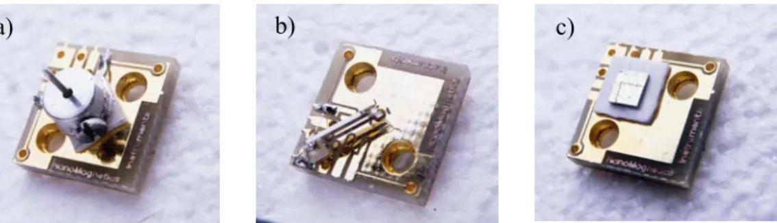
Our experimental setup also can work in three modes with three different SPM probes: STM, AFM and SHPM. (Figure 2-5)
Figure 2.5: Available SPM probes: a) STM holder, b) Quartz Tuning Fork AFM probe, c) SHPM probe.
Another part of our experimental setup is a homemade cryostat system that was build by our under-grad student Duygu Can (Figure 2.6). This cryostat system is used for the controlled cooling down and warming up processes. Temperature changing rate is very critical for the LT-SHPM system because of the piezoelectric materials and quartz tube. The cooling rate should be smaller
b)
than 2K/minute. It is also possible to fix the temperature at specific point and fix the temperature change rate with the help of the Oxford Research System’s ITC 601 controller. This controller is programmed by Objectbench software.
Figure 2.6: Our homemade cryostat system which is directly inserted to the liquid nitrogen tank.
Chapter 3
SHPM Probe Fabrication
The Hall Probes are micro fabricated devices. As it is discussed in Chapter 1, they are based on Hall Effect on a cross effective area which is limited with the 4 arms of the probe. To observe a Hall Effect on the material, the material should be conductive. The high carrier concentration decreases the Hall coefficient and the sensitivity of the probe. The high mobility enables one to pass current without heating the sensor. Then for an optimum measurement, semiconductors are used to fabricate the Hall Probes. Thin semiconductor films on insulating wafer or 2DEG wafers can be used. Other advantages of using thin films or 2DEG wafers are limiting the measurement area on the z direction. Otherwise the measurement takes the average of the magnetic field that penetrates to the probe. In this thesis work, a P-HEMT wafer was used for probe fabrication. The structure and the specifications of this wafer are given in Figures 3.1 and 3.2.
9 Å AlAs 1000 Å N+ (1013cm-2) 9 Å Undoped AlAs 230 Å Undoped AlGaAs Si Pulse (4.4 1012) 20 Å Undoped AlGaAs 20 Å Undoped InlGaAs 4500 Å SLB Pseudomorphic layer Substrate with Low DX centers
Figure 3.1: Pseudomorphic High Electron Mobility Transistor P-HEMT wafer and its specifications that is used for Hall Probe fabrication
Photolithography and e –beam lithography are commonly used for fabrication of Hall Probes. These techniques are based on masking the samples and etching or making metallization using lift-off process after this.
Figure 3.2: Hall Probe with integrated STM tip
Photolithography is the process of “writing” on a surface using light. The process is extremely simple and consists of only a few steps. The initial step in photolithography is to cover a substrate with a polymer photoresist that changes its properties upon exposure to certain wavelength of light. First, the resist is dissolved in a liquid solvent. Second, the resist is placed drop wise onto the substrate surface and spun at speeds between 1,000-10,000 rpm. This process, called spin coating, allows for control of resist thickness of the substrate by varying the rotation speed. The higher the rotation rate the thinner the resist layer. Third, the substrate is baked on a hot plate to force off the solvent leaving behind a resist layer. This resist layer is adsorbed to the surface by a weak interaction arising from Van der Waals forces. This weakness is advantageous for a couple reasons: one, using a polymer that would chemically bond to the substrate surface could change or damage desired surface features; two, it is advantageous for the process to be easily reversible, allowing for a complete stripping of the resist from the substrate by a solvent wash called a developer.
STM Tip Part
Effective Area
Figure 3.3: Photolithography process
The resist layer is then irradiated through a pattern mask that is either in contact with the resist layer or held at a significant height above the surface. The photoresist exposed to radiation undergoes a structural change, and its solubility changes as a result. If the exposed resist becomes soluble to the developer, it is referred to as the positive resist; if it becomes less soluble, it is called the negative resist.
Figure 3.4: Difference of negative and positive resists
After exposure to radiation, a pattern is left on the resist layer consisting of the altered polymers. The entire resist layer is then treated with a developer that
removes either the exposed or unexposed resist material depending upon the solubility of the resist used. The substrate below the resist layer is thus exposed.
The exposed substrate material is then treated with some processes such as etching, metal deposition, or ion implantation that does not interact with the resist material. Finally, the resist material is completely stripped away with another solvent wash, typically acetone. This process can be repeated several times to build layers of features onto the substrate surface.
Figure 3.5: Etch process after photolithography
There are various ways of etching the wafer by different methods. Most preferred method is a physical etching, which is done by reactive ion bombardment of the surface called reactive ion etching (RIE). This technique gives possibility to etch the wafer from the surface to inside very uniformly and precisely to a desired value. The high energy ion bombardment can cause etching on the undesired regions of the wafer, moreover it consumes various enchant gases. Therefore we do the etching process by means of chemical etch using an acidic solution that is called wet etching technique. In this technique, the chemicals etch the surface. Although the chemical etch is simpler, the side etch problem occurs during the etching, because of the etching through the crystallographic directions. During etching process, the pattern, that we do not want to etch are protected by the photoresist material.
In our case, the first step is the Hall Probe definition with using these two techniques. For this purpose, first our wafer is cut into (5mm x 5mm) pieces with the help of a diamond scriber. To avoid the damage the surface of our wafer, the wafer can be coated with a thick layer of photoresist before this process. After the wafer is cut; the pieces, that will be used, are washed first with acetone and then with propanol-2. Then the wafer is dried with dry N2 gas
without giving permission to propanol-2 dry naturally. This drying process avoids the defects that can be caused by the residues of the chemicals. After the cleaning process the wafer is coated with photoresist (AZ5214) by spinning at 10,000 rpm. Then it is baked at 110 ºC for 50 seconds by using a hotplate, which is known as soft bake. In the next step the wafer is placed under the mask at the mask aligner (Karl Suss, MJB 3). After a good alignment with the mask aligner, the powerful UV light with 5mW is exposed to the surface for about 35 or 40 seconds. Then the wafer is developed by watching the color changes at the surface. When the fast color change is finished the wafer is washed in a fresh de-ionized water to remove the developer chemical on it. The development process takes about 15 second for the given photoresist thickness and exposure time.
Figure 3.6: Hall Probe definition with photoresist coating, after develop
The Hall Probe definition that coated with photoresist is examined under a powerful optical microscope. If developed pattern is satisfactory, the etching chemicals or the RIE is getting prepared. For the chemical wet etching, the
usual chemicals for the Hall Probe definition are H2SO4, H2O2 and H2O. The
mixture is prepared by using these chemicals with the ratio 1:8:320, respectively. But in this thesis work, a problem is occurred during wet etching process which is what we think caused by the wafer quality. Then for a second choice, we used Reactive Ion Etching (RIE) system for the Hall Probe definition with 20 sccm CCl2F2. The parameters can be given as 30 second for gas condition time and 74
W in 4x10⁻³ mbar pressure. To measure the etch rate, an unused part of the sample is used. The etch rate is determined as 15.7Å/sec. Then our developed wafers are etched for 2 min and 10 second (~200 nm) to pass the 2DEG layer which is located about 180 nm down from the wafer surface.
Figure 3.7: Hall Probe definition after RIE etch
As the second step in Hall Probe fabrication the mesa etch is done with using same procedure. By this step, we separate the Hall Probes on the wafer with sharp edges. This is also important for this thesis work where the corner of the mesa is used as the sharp tip for the AFM feed-back. In this time, parameters are changed as 6,000 rpm for the spin, and 20 minutes for the mesa etch time with RIE for 1.8µm. A very important point for this step is the alignment. The mesa mask should be located precisely aligned with respect to the Hall Probe definition. The mesa mask hides the Hall probe definitions to protect from the light, and then a real challenge is occurred at this step. For this reason the turns of the micrometer screws of the mask aligner is recorded carefully for the
alignment in x and y directions and then alignment is done blindly just with these records.
Figure 3.8: Mesa Etch by RIE
For the third step of Hall probe fabrication the recess etch is done similarly. This step is done to avoid the shorting of the sample and the Hall Probe’s electrical connections during the SHPM experiment. So the edges close to the sides of the Hall probes is etched about 50-60 µm deep in this step. For the lithography part the wafer is spun at 6,000 RPM again, and exposed for 60 seconds. To avoid the undercut etch, a mask is used with gear tooth like edges. The sides of the mask are aligned carefully to locate the Hall Probes at the centre of the light protective area. After development the sides of the wafer is cleaned by acetone with help of a Q-tip and an extra photoresist drop is applied on the centre of the wafer over the thick photoresist layer that left after development. Because the etch depth is so high, the HCl is used with ratio 4 HCl, 10 Hydrogen peroxide, 55 DI water for 1 hour period.
The last step in Hall Probe fabrication for this thesis work is the metallization. In order to have an ohmic contact behavior of the contact of metal and GaAs, the metal should be defused or alloyed into the GaAs wafer. Ohmic behavior means linear dependence of the current passing through the contact on the voltage applied across the contact. A good ohmic contact possesses low resistance, long endurance in time and high stability against temperature. The common technique used for the ohmic contact is to coat metal film through exposed and developed sample the photolitogrpahed sample, lift-off photo resist and unwanted metals and alloy the metal into GaAs by Rapid Thermal Processing (RTP).
For this purpose the wafer is again coated with AZ 5214 resist by spinning at 10,000 RPM. The metallization mask is carefully aligned as in mesa step. In this step, Hall Probe part and the ways between the connection paths are protected by the mask. Then the photoresist is removed only from the connection paths after development. After these preparations are finished, we metallize the whole wafer by using the box-coater (Leybold, LE 560). Box-coater thermally evaporates the material in the high vacuum and deposits its vapor into the wafer surface. The used vacuum condition is about 10-6 mbar and the wafer is hold about 20 cm above the metal boats. Our process involves multilayered metal deposition with Ge dopant included in between layers. Ge will play the role for obtaining ohmic behavior of the contact after the layers are alloyed into GaAs. Ni and thin Au layers are deposited to help Ge penetrating into GaAs. 1,500A0 Au layer is deposited for increasing the conductivity for and easy bonding. For next step after the metallization of Ti, Au and Ge layers, photoresist is lifted-off with the metals on it. Metallized wafer is put into acetone to dissolve PR (photoresisit). Since PR is dissolved in the acetone the metal parts on PR become free and float in the acetone where the metal parts of the bare wafer stay. This procedure is called the lift off. At the end, the desired patterns are obtained on the surface of GaAs wafer. Ohmic contact formation
after photolitography as mentioned before a cleaning process is essential before passing the next step which is RTP. Cleaning is performed by the previously described washing with acetone and propanol-2 method. RTP is generally named annealing or rapid thermal annealing RTP. This is thermal process in which the wafer can be annealed by blackbody radiation of a filament.
Figure 3.10: Metallization development.
Figure 3.11: Doped Au layer after RTP process on Hall Probe contacts
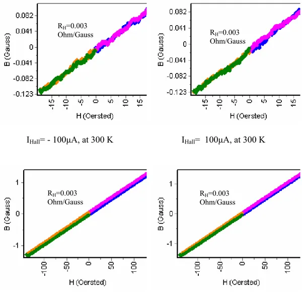
For the STM feed-back SHPM Hall Probes, the tip metallization can be done before the final cutting step. But for this thesis we ignore this step. The finished Hall probe’s photograph is given in Figure 3.12 and B-H curves are given in Figure 3.13.
Figure 3.12: Finished Hall Probe without STM Tip.
IHall= - 100µA, at 300 K IHall= 100µA, at 300 K
IHall= - 100µA, at 77 K IHall= - 100µA, at 77 K
Figure 3.13: B-H curves of Hall probes that are fabricated during this thesis work. RH=0.003 Ohm/Gauss RH=0.003 Ohm/Gauss RH=0.003 Ohm/Gauss RH=0.003 Ohm/Gauss
39
Chapter 4
Scanning Hall Probe Microscopy
(SHPM) experiments with STM
feedback
In SHPM, a micro-fabricated Hall sensor is positioned very close to the surface for measuring very small magnetic field data. It is known that the magnetic field strength is decreasing with 1/r3, where r is the distance between the probe and the surface. So the distance between the surface and the probe is very important for not losing the field strength.
Figure 4.1: Hall Probe with STM Tip. STM Tip
Therefore SHPM technique should be combined with other SPM techniques as STM or AFM. The STM tracking mechanism is the simpler one for this purpose. A STM tip or in other words a gold coated mesa corner for tunneling can be located near the SHPM probe as given in Figure 4.1. Because this gold coated mesa corner is used for STM feedback mechanism in our system, the sample should be given an angle about 1.25º to make the STM tip closest to the surface than anything else (Figure 4.2). The sample must be conductive STM tracking SHPM. For the non-conductive samples, 10 or 20 nm thick Au layer can be coated on the sample surface.
Figure 4.2: Alignment angle for SHPM operation.
To give the correct angle between the probe and the surface, a careful alignment procedure is employed. The sample is fixed to the slider puck with three springs for this purpose. One of these springs is located to the end corner of the SHPM probe just to align the angle as shown in Figure 4.2. First of all, using the three screws, the probe is made parallel to the surface. Then using the screw at the bottom is loosened to give desired tilt angle.
Sample
PCB Hall Probe
1-1.25° Bond Wires
Figure 4.3: Schematic of alignment mechanism.
Figure 4.4: Images of the hall probe and its reflection from the sample surface: a) from the first side after get parallel to the surface, b) from the second side after
get parallel to the surface, c) after the tilt angle is given.