NOVEL OPTICAL ANTENNAS INSPIRED
BY METAMATERIAL ARCHITECTURES
A THESIS
SUBMITTED TO THE DEPARTMENT OF ELECTRICAL AND ELECTRONICS ENGINEERING
AND THE GRADUATE SCHOOL OF ENGINEERING AND SCIENCES OF BILKENT UNIVERSITY
IN PARTIAL FULLFILMENT OF THE REQUIREMENTS FOR THE DEGREE OF
MASTER OF SCIENCE
By
Veli Tayfun Kılıç
August 2011
I certify that I have read this thesis and that in my opinion it is fully adequate, in scope and in quality, as a thesis for the degree of Master of Science.
Assoc. Prof. Dr. Hilmi Volkan Demir (Supervisor)
I certify that I have read this thesis and that in my opinion it is fully adequate, in scope and in quality, as a thesis for the degree of Master of Science.
Assoc. Prof. Dr. Vakur B. Erturk
I certify that I have read this thesis and that in my opinion it is fully adequate, in scope and in quality, as a thesis for the degree of Master of Science.
Prof. Dr. Sencer Koc
Approved for the Graduate School of Engineering and Sciences:
Prof. Dr. Levent Onural
ABSTRACT
NOVEL OPTICAL ANTENNAS INSPIRED BY
METAMATERIAL ARCHITECTURES
Veli Tayfun Kilic
M.S. in Electrical and Electronics Engineering
Supervisor: Assoc. Prof. Dr. Hilmi Volkan Demir
August 2011
The spatial resolution of conventional optical systems is commonly constrained by the diffraction limit. This is a fundamental problem important for various high-tech applications including density limitation in data storage devices (CD, DVD, and Blue-ray discs), crosstalk in detectors, and blurred images in microscopy. To overcome this limit, different types of optical antennas have been investigated to date. However, these antennas either do not exhibit a maximum level of field intensity enhancement that can be achieved via field localization using plasmons or they have large field intensity enhancement at the cost of complicated three-dimensional architectures or very sharp tips, which are hard to fabricate. In this thesis, to address this problem, we investigate a new class of planar optical antennas inspired by metamaterial architectures including E-shape and comb shape. We found that the field intensity enhancements inside the gap regions of such comb-shaped nanoantennas were significantly increased compared to the single or array of dipoles, despite operating across an electrical length significantly reduced with respect to their resonance wavelength. We also showed that the field intensity localization of a single dipole nanoantenna can be at least doubled using single ring resonator with the same gap size by decreasing field radiations from end points and obtaining continuous current flow. These results indicate that comb-shaped planar nanoantennas hold great promise for strong field localization.
Keywords: Optical antennas, split ring resonator, comb-shape, dipole,
ÖZET
METAMALZEME MİMARİLERİNDEN
ESİNLENİLEREK OLUŞTURULAN ORİJİNAL OPTİK
ANTENLER
Veli Tayfun Kılıç
Elektrik ve Elektronik Mühendisliği Bölümü Yüksek Lisans Tez Yöneticisi: Doç. Dr. Hilmi Volkan Demir
Ağustos 2011
Geleneksel optik sistemlerin çözünürlükleri genellikle kırılım limiti ile sınırlıdır. Bu; bir çok yüksek teknoloji uygulamalarında CD, DVD ve mavi ışın diskleri gibi veri depolayıcı aletlerin kapasitelerinin sınırlı olması, dedektörlerdeki sinyal karışmaları, bulanık mikroskopik görüntüler gibi önemli sorunlara neden olur. Bu problemin üstesinden gelebilmek amacıyla günümüze dek bir çok farklı türde optik anten çalışılmıştır. Ancak, bu antenler ya plazmonların ışığı odaklaması ile elde edilebilecek en yüksek dalga şiddetine sahip değiller ya da üretimi zor olan karmaşık 3 boyutlu yapılara veya çok sivri uçlara sahiplerdir. Bu tezde bu probleme karşılık olarak metamalzeme mimarilerinden esinlenilerek oluşturulan E ve tarak şekilleri kullanan yenilikçi düzlemsel optik antenleri çalıştık. Rezonans dalga boyuna kıyasla elektriksel uzunluğu önemli ölçüde küçük olmasına rağmen, bağlı tarak şeklindeki nanoantenlerin boşluklarında odaklanan ışığın şiddetinin tek veya sıra halindeki dipollerin boşluklarında odaklanan ışığın şiddetinden önemli ölçüde fazla olduğunu bulduk. Ayrıca, dipol nanoantendeki odaklanan ışığın şiddetinin aynı boşluğa sahip tek halka rezonatör şeklindeki anten ile uç noktalardan yayılan ışığı azaltmak ve akımın kesintisiz akmasını sağlamak suretiyle iki katından fazlasına çıkarılabileceğini gösterdik. Bu sonuçlar şunu göstermektedir ki tarak şeklindeki düzlemsel nanoantenler ışığın güçlü bir şekilde odaklanması açısından büyük umut vaat etmektedir.
Anahtar Kelimeler: Optik antenler, yarık halka resonatörler, tarak şekli, dipol,
Acknowledgements
I would like to express my deepest gratitude to my supervisor Assoc. Prof. Dr. Hilmi Volkan Demir for his guidance and support throughout my M.S. study. He was always helpful and kind to me and I am indebted to him for allowing time whenever I need, even if he was very busy.
I would like to thank Assoc. Prof. Dr. Vakur B. Erturk for his contributions and guidance during my research efforts. He was like my second supervisor. I am indebted to him for giving very useful comments and suggestions during our meetings.
I would also like to thank Prof. Dr. Sencer Koc for reading and commenting on this thesis and for being a member of my thesis committee on this hot August day.
I am very proud to dedicate my thesis to my mother; Necla Kilic, my father; Samet Kilic and my brother; Ismail Kilic for their endless love and endless supports in my whole life. The words are not enough to describe my love and acknowledgement to them.
I would like to thank Tubitak (The Scientific and Technological Research Council of Turkey) for their financial support during my M.S. study.
I would also like to thank Bilkent University EE Department and especially Ihsan Dogramaci the founder of our University (I pray for him) for their contributions and providing such good circumstances during both my undergraduate and graduate study.
I would like to thank former and recent members of Demir Research Group. I would especially like to thank Mustafa Akin Sefunc, Ugur Karatay, Ozan Yerli, Emre Unal, Ozgun Akyuz, Sayim Gokyar, Kivanc Gungor, Hatice Ertugrul, Can Uran, Talha Erdem, Burak Guzelturk, Ahmet Fatih Cihan, Shahab Akhavan, Yusuf Kalestemur, Sedat Nizamoglu, Evren Mutlugun, Emre Sari, Nihan Kosku Perkgoz, Urartu Seker, Pedro L. Hernandez, Onur Akin and Refik Sina Toru for their friendship and collaborations.
Lastly, I cannot pass without mentioning some of my colleagues` names. I am really grateful to my office friends; Ismail Uyanik, Ali Nail Inal, Deniz Kerimoglu, Naci Saldi, Gunes Bayir, Mahmut Yavuzer, Samet Guler for our wonderful late night studies and also to my friends from department; M. Kenan Ozel, Hasan Hamzacebi, Cagri Goken for their support and good friendship.
Table of Contents
ACKNOWLEDGEMENTS ... VII
TABLE OF CONTENTS ... IX
LIST OF FIGURES ... XI
LIST OF TABLES ... XVI
1. INTRODUCTION ... 1
2. FUNDAMENTALS OF PLASMONICS ... 7
2.1BRIEF HISTORY ... 8
2.2SURFACE PLASMON POLARITONS ... 10
2.3LOCALIZED SURFACE PLASMONS ... 22
2.4PLASMONICS IN OPTICAL ANTENNAS ... 23
2.5FINITE-DIFFERENCE TIME-DOMAIN (FDTD)METHOD AND SIMULATION TOOL LUMERICAL ... 26
3. FIELD ENHANCEMENT AND SURFACE CURRENT RELATIONS ... 29
3.1METHOD AND GEOMETRY ... 30
3.2SIMULATION RESULTS AND DISCUSSION ... 32
3.2.1SINGLE DIPOLE ... 32
3.2.2DOUBLE DIPOLES (WITH S =100 NM CENTER-TO-CENTER DISTANCE) ... 38
3.2.3DOUBLE C-SHAPE (WITH S =100 NM CENTER-TO-CENTER DISTANCE)
... 39
3.2.4SPLIT RING RESONATOR (SRR)SHAPE (CONNECTED DOUBLE C-SHAPES) (WITH S =100 NM CENTER-TO-CENTER DISTANCE) ... 44
3.3CONCLUSION ... 57
4. PARAMETRIC STUDIES OF DIPOLE ANTENNAS VS. SRR- AND COMB-SHAPED ANTENNAS ... 60
4.1DIPOLE ANTENNA VS.SRR-SHAPED ANTENNA ... 61
4.1.1METHOD AND GEOMETRY ... 61
4.1.2SIMULATION RESULTS AND DISCUSSIONS... 62
4.1.3CONCLUSION ... 69
4.2VARIOUS ANTENNA ARCHITECTURES FROM A SINGLE DIPOLE TO COMB -SHAPED ANTENNA... 70
4.2.1METHOD AND GEOMETRY ... 70
4.2.2SIMULATION RESULTS AND DISCUSSIONS... 72
4.2.3CONCLUSION ... 84
5. CONCLUSIONS ... 86
List of Figures
Figure 1.1: (a) Light focusing by a positive converging lens, (b) Energy distribution of focused light (Airy disk) (the images were taken from “http://www.wikipremed.com/” and “http://spie.org/”, respectively). ... 1 Figure 2.1: The Lycurgus Cup in British museum without direct illumination (left) and under direct illumination (right) (photos were taken from “http://www.britishmuseum.org/explore/highlights/highlight_objects/pe_ml a/t/the_lycurgus_cup.aspx”). ... 8 Figure 2.2: Simple metal-dielectric boundary. ... 13 Figure 2.3: Surface plasmon polaritons for TM modes (captured from
“http://ralukaszew.people.wm.edu/new_projects.htm”). ... 18 Figure 2.4: Refraction of light at a boundary. ... 19 Figure 2.5: General relative permittivity vs. angular frequency for metal and
dielectric. ... 21 Figure 2.6: Dispersion relations of SPPs. ... 21 Figure 2.7: Simple dipole antenna geometry. ... 24 Figure 2.8: Simulated localized surface plasmons and field radiations (left),
along with the cross-section of dipole antenna (right). ... 25 Figure 2.9: A screenshot taken from our simulations showing Lumerical
software user interface. ... 27 Figure 3.1: Single dipole antenna geometry. ... 31 Figure 3.2: Single dipole antenna geometry. ... 32 Figure 3.3: Field intensity enhancement with respect to optical wavelength. ... 32 Figure 3.4: Magnetic field component intensities at 765 nm on constant x
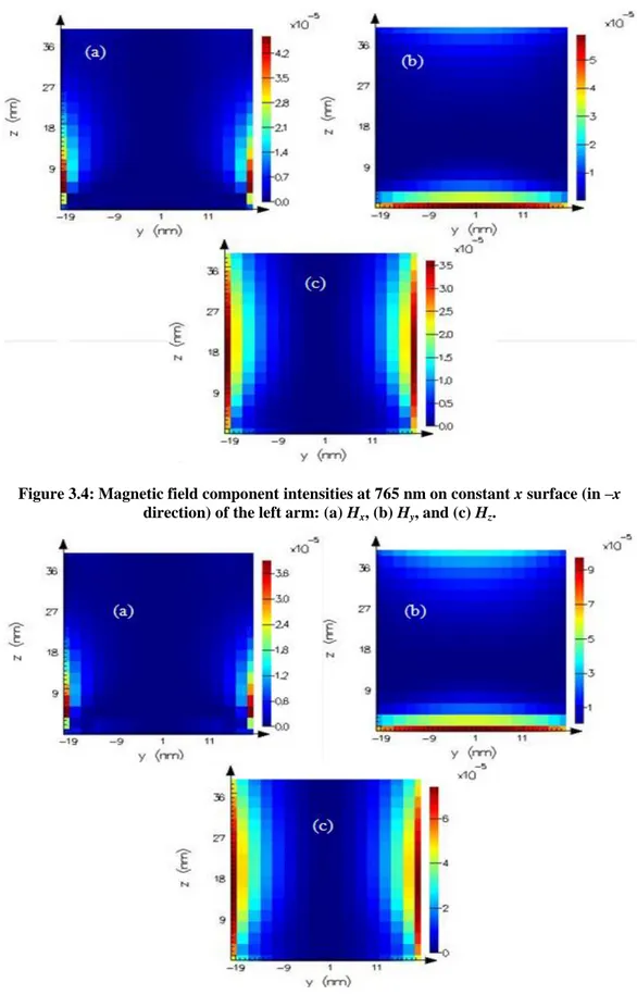
surface (in –x direction) of the left arm: (a) Hx, (b) Hy, and (c) Hz. ... 34
Figure 3.5: Magnetic field component intensities at 765 nm on constant x surface (in +x direction) of the left arm: (a) Hx, (b) Hy, and (c) Hz. ... 34
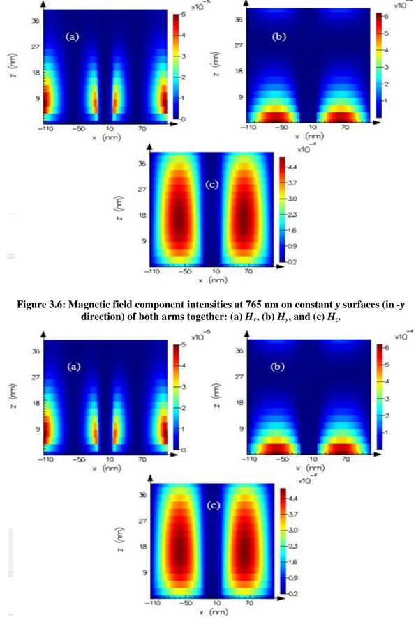
Figure 3.6: Magnetic field component intensities at 765 nm on constant y surfaces (in -y direction) of both arms together: (a) Hx, (b) Hy, and (c) Hz. 35
Figure 3.7: Magnetic field component intensities at 765 nm on constant y surfaces (in +y direction) of both arms together: (a) Hx, (b) Hy, and (c) Hz.
... 35
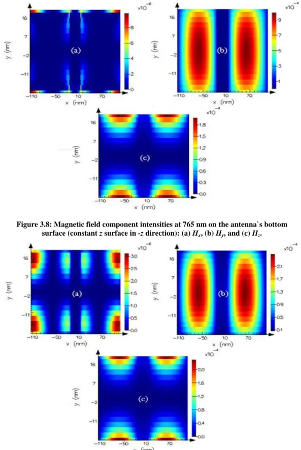
Figure 3.8: Magnetic field component intensities at 765 nm on the antenna`s bottom surface (constant z surface in -z direction): (a) Hx, (b) Hy, and (c) Hz. ... 36
Figure 3.9: Magnetic field component intensities at 765 nm on the antenna`s top surface (constant z surface in +z direction): (a) Hx, (b) Hy, and (c) Hz. ... 36
Figure 3.10: Dominant tangential magnetic fields on the surfaces of the dipole arm. ... 37
Figure 3.11: Double dipoles with s=100 nm center-to-center distance. ... 38
Figure 3.12: Field intensity enhancement of the double dipoles. ... 38
Figure 3.13: Double C-shape antenna structure (with s=100 nm center-to-center distance and w=40 nm width). ... 40
Figure 3.14: Field intensity enhancement of double C-shape pair. ... 40
Figure 3.15: Top perspective of our double C-shape antenna. ... 41
Figure 3.16: Dominant tangential field components. ... 43
Figure 3.17: Surface current flows on double C-shaped antenna (on right part) (J= nxH). ... 43
Figure 3.18: SRR-shaped antenna structure. ... 44
Figure 3.19: Field intensity enhancement of SRR. ... 44
Figure 3.20: Top view of our SRR-shaped antenna. ... 45
Figure 3.21: Magnetic field component intensities at 2160 nm on constant x=15 nm surface of antenna part 1 right arm: (a) Hx, (b) Hy, and (c) Hz. ... 46
Figure 3.22: Magnetic field component intensities at 2160 nm on constant y=30 nm surface of antenna part 1: (a) Hx, (b) Hy, and (c) Hz. ... 47
Figure 3.23: Magnetic field component intensities at 2160 nm on constant y=70 nm surface of antenna part 1: (a) Hx, (b) Hy, and (c) Hz. ... 47
Figure 3.24: Magnetic field component intensities at 2160 nm on constant z=0
nm (bottom) surface of antenna part 1: (a) Hx, (b) Hy, and (c) Hz. ... 48
Figure 3.25: Magnetic field component intensities at 2160 nm on constant z=40
nm (top) surface of antenna part 1: (a) Hx, (b) Hy, and (c) Hz. ... 48
Figure 3.26: Magnetic field component intensities at 2160 nm on constant x=75
nm surface of the right connection part: (a) Hx, (b) Hy, and (c) Hz. ... 50
Figure 3.27: Magnetic field component intensities at 2160 nm on constant
x=115 nm surface of the right connection part: (a) Hx, (b) Hy, and (c) Hz. 50
Figure 3.28: Magnetic field component intensities at 2160 nm on constant z=0
nm (bottom) surface of the right connection part: (a) Hx, (b) Hy, and (c) Hz.
... 51 Figure 3.29: Magnetic field component intensities at 2160 nm on constant z=40
nm (top) surface of the right connection part: (a) Hx, (b) Hy, and (c) Hz. ... 51
Figure 3.30: Magnetic field component intensities at 2160 nm on constant y=-30
nm surface of antenna part 2: (a) Hx, (b) Hy, and (c) Hz. ... 53
Figure 3.31: Magnetic field component intensities at 2160 nm on constant y=-70
nm surface of antenna part 2: (a) Hx, (b) Hy, and (c) Hz. ... 53
Figure 3.32: Magnetic field component intensities at 2160 nm on constant z=0
nm (bottom) surface of antenna part 2: (a) Hx, (b) Hy, and (c) Hz. ... 54
Figure 3.33: Magnetic field component intensities at 2160 nm on constant z=40
nm (top) surface of antenna part 2: (a) Hx, (b) Hy, and (c) Hz. ... 54
Figure 3.34: Surface currents on SRR-shaped antenna (only its half shown due to the symmetry). ... 56 Figure 4.1: Optical antenna architectures based on split ring resonator (SRR) (a) and single dipole structure (b). ... 62 Figure 4.2: Computed field intensity enhancement profiles for the SRR (a) and
the dipole (b). In (a) the results of SRR for l=190, 150 and 110 nm are represented starting from the top to the bottom, respectively, with their zero levels shifted for clarity. ... 63 Figure 4.3: Resonance wavelength shift of the SRR antenna (a) with length s in
Figure 4.4: (a) Maximum field enhancement dependency on antenna geometries and (b) resonant wavelength shift with the current path length (L) in the
SRR antenna architecture. ... 65
Figure 4.5: (a) Maximum field enhancement level and (b) resonance wavelength shift as a function of the dipole antenna length d. ... 67
Figure 4.6: Maximum field enhancement vs. resonance wavelength for single dipole and SRR antennas. ... 68
Figure 4.7: Improvement factor vs. wavelength for our SRR antenna with respect to single dipole antenna. ... 68
Figure 4.8: Architecture of single connected comb antenna with 2 teeth. ... 71
Figure 4.9: Single dipole antenna geometry. ... 72
Figure 4.10: Double dipoles with s=100 nm center-to-center distance. ... 73
Figure 4.11: Double C-shape antenna structure (with s=100 nm center-to-center distance). ... 73
Figure 4.12: SRR shape antenna structure (with s=100 nm center-to-center distance). ... 74
Figure 4.13: Double dipoles with s=200 nm center-to-center distance. ... 74
Figure 4.14: Double C-shape antenna structure (with s=200 nm center-to-center distance). ... 75
Figure 4.15: SRR shape antenna structure (with s=200 nm center-to-center distance). ... 75
Figure 4.16: Triple dipoles with s=100 nm center-to-center distances. ... 76
Figure 4.17: Double E-shape antenna structure (with s=100 nm center-to-center distance). ... 76
Figure 4.18: Single connected double E-shape antenna structure (with s=100 nm center-to-center distances). ... 77
Figure 4.19: Double connected double E-shape antenna structure with a single gap at the end (with s=100 nm center-to-center distance). ... 77
Figure 4.20: Double connected double E-shape antenna structure with a single gap at the center (with s=100 nm center-to-center distances). ... 78
Figure 4.22: Double E-shape antenna structure (with s=200 nm center-to-center distances). ... 79 Figure 4.23: Single connected double E-shape antenna structure (with s=200 nm
center-to-center distances). ... 80 Figure 4.24: Double connected double E-shape antenna structure with a single
gap at the end (with s=200 nm center-to-center distances). ... 80 Figure 4.25: Double connected double E-shape antenna structure with a single
gap at the center (with s=200 nm center-to-center distance). ... 81 Figure 4.26: Connected comb antenna geometry with 3 teeth (with s=100 nm
center-to-center distances). ... 82 Figure 4.27: Connected comb antenna geometry with 4 teeth (with s=100 nm
center-to-center distances). ... 82
List of Tables
Table 1.1: Physical parameters and storage capacities of optical disc systems in chronological order [2]. ... 2 Table 4.1: Peak field enhancement and resonance wavelength inside the gap
region of the single dipole antenna. ... 73 Table 4.2: Peak field enhancement and resonance wavelength inside the gap
regions of the double dipole antennas (with s=100 nm). ... 73 Table 4.3: Peak field enhancement and resonance wavelength inside the gap
regions of the double C-shape antenna (with s=100 nm). ... 73 Table 4.4: Peak field enhancements and resonance wavelengths inside the gap
region of the SRR shape antenna (with s=100 nm). ... 74 Table 4.5: Peak field enhancement and resonance wavelength inside the gap
regions of the double dipole antennas (with s=200 nm). ... 74 Table 4.6: Peak field enhancements and resonance wavelengths inside the gap
regions of the double C-shape antenna (with s=200 nm). ... 75 Table 4.7: Peak field enhancements and resonance wavelengths inside the gap
region of the SRR shape antenna (with s=200 nm). ... 75 Table 4.8: Peak field enhancements and resonance wavelengths inside the gap
regions of the triple dipoles antenna (with s=100 nm). ... 76 Table 4.9: Peak field enhancements and resonance wavelengths inside the gap
regions of the double E-shape antenna (with s=100 nm). ... 76 Table 4.10: Peak field enhancements and resonance wavelengths inside the gap
regions of the single connected double E-shape antenna (with s=100 nm). ... 77 Table 4.11: Peak field enhancements and resonance wavelengths inside the gap
region of the double connected double E-shape antenna with a single gap at the end (with s=100 nm). ... 78
Table 4.12: Peak field enhancements and resonance wavelengths inside the gap region of the double connected double E-shape antenna with a single gap at the center (with s=100 nm). ... 78 Table 4.13: Peak field enhancements and resonance wavelengths inside the gap
regions of the triple dipoles antenna (with s=200 nm). ... 79 Table 4.14: Peak field enhancements and resonance wavelengths inside the gap
regions of the double E-shape antenna (with s=200 nm). ... 79 Table 4.15: Peak field enhancements and resonance wavelengths inside the gap
regions of the single connected double E-shape antenna (with s=200 nm). ... 80 Table 4.16: Peak field enhancements and resonance wavelengths inside the gap
region of the double connected double E-shape antenna with a single gap at the end (with s=200 nm). ... 81 Table 4.17: Peak field enhancements and resonance wavelengths inside the gap
region of the double connected double E-shape antenna with a single gap at the center (with s=200 nm). ... 81 Table 4.18: Peak field enhancements and resonance wavelengths inside the gap
regions of the connected comb shaped antenna with 3 teeth (with s=100 nm). ... 82 Table 4.19: Peak field enhancements and resonance wavelengths inside the gap
regions of the connected comb-shaped antenna with 4 teeth (with s=100 nm). ... 83
Chapter 1
Introduction
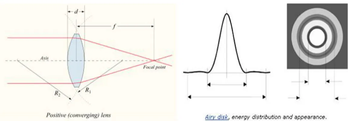
The spatial resolution of a conventional optical system is constrained by the diffraction limit of λ/2NA given the operating optical wavelength λ and the numerical aperture NA of the system [1]. Figure 1.1 illustrates the focusing of light through a lens and shows energy (or intensity) distribution of the focused light.
Figure 1.1: (a) Light focusing by a positive converging lens, (b) Energy distribution of focused light (Airy disk) (the images were taken from “http://www.wikipremed.com/” and
This diffraction limit gives rise to important problems in a number of applications including limited density in data storage, blurred images in microscopy and crosstalk in detectors. Since the diffraction limit is directly proportional to the wavelength of light, to cope with these limits, shorter and shorter wavelengths are being used as the associated technologies improve over time. For instance, to increase capacity of the data storage devices blue wavelength lasers are taking place of old CD lasers today. This development in optical data storage devices is tabulated in Table 1.1. However, despite using shorter and shorter wavelength, the fundamental limit is not overcome in such conventional optical systems.
System Year λ [μm] N0 λ/N0 [μm] Capacity [GB/layer] Diameter [cm] Playing time [min.] Video long play 1978 0.633 0.40 1.56 4.5 30 30-60 Laser disc 1983 0.785 0.50 1.57 4.5 30 60 Compact disc 1983 0.785 0.45 1.74 0.65 12 74 DVD 1995 0.650 0.60 1.08 4.7 12 135 HD-DVD 2006 0.405 0.65 0.62 16 12 135 Blu ray 2006 0.405 0.85 0.48 23 12 135
Table 1.1: Physical parameters and storage capacities of optical disc systems in chronological order [2].
However, the production and handling of such blue ray lasers are difficult and costly. In addition, since the diffraction limit is approximately half of the wavelength, light focusing is still constrained within a size of 100 nm`s. Therefore, another technique is required to confine light in a region far beyond the diffraction limit.
Plasmonics offers a solution to meet this requirement. Today it is one of the leading topics in the area of nanophotonics. In terms of physics, we can understand plasmons as collective charge oscillations or free electron gases in metals. Plasmonics investigates how the electromagnetic field can be confined in a region smaller than the wavelength [3,4].
The interaction between radiating electromagnetic fields and conduction electrons on metallic surfaces leads to a field localization. Such plasmonic interactions are of fundamental importance as they allow for confining fields beyond the diffraction limit [4-6]. As a result,today plasmonics is exploited in a wide range of applications including plasmon waveguides, subwavelength apertures for enhanced optical transmission, optical nanoscale antennas, plasmon enhanced Raman scattering, surface-plasmon-polariton-based sensors and plasmonic integrated circuits [4-7].
Although plasmonic applications such as transmission apertures and waveguides help us to confine light in a region smaller than the diffraction limit, the low intensity field may pose a problem. Typically, the resultant electromagnetic excitations die out very quickly as we move farther. Therefore, obtaining higher field intensity is a necessity for plasmonic applications. Plasmonic structures such as optical nanoantennas accomplish this demand by obtaining field spots with very high intensities in a region beyond the diffraction limit [8]. Consequently, they offer a wide variety of important applications including scanning near field optical microscopy, ultra-high density data storage and very sensitive optical detectors.
To this end, different types of optical antennas have been widely investigated [9-27]. Among them dipole and related architectures have been studied most extensively thanks to their simple geometries [10-18]. Their spectral response, tuned by the material parameters (metal, substrate, medium) as well as the geometrical parameters (antenna length, gap size, etc.), have been numerically
computed and experimentally observed. Unfortunately, the field enhancement obtained in these dipole antennas has not reached the largest possible levels that can be achieved using such plasmonic interactions unless very sharp tips, which are difficult to fabricate, are used. Also, nanoantennas of different shapes such as spherical [19-21] and elliptical [20-22] antennas have been reported. For example, three-dimensionally V-shaped structures [23] have been shown to lead to higher enhancement levels. However, while this kind of three-dimensional architectures are capable of providing larger peak field intensity in their localized regions, they are unfavorably harder to fabricate due to their relatively complex construction. Consequently, challenging fabrication of sharp tips or 3D structures hindered the application of large field enhancement in practical architectures. Therefore, there is now a strong need to enable high field enhancement levels while sustaining relatively simple, planar fabrication at the same time.
To address this problem, in this thesis, we study and demonstrate planar optical antennas based on split ring resonator (SRR) architectures. Although various forms and variants of SRRs have been extensively studied especially for metamaterials till date [28], there is no prior report that links SRR antennas evolving from dipole antennas for their capabilities of field localization. This work provides a comparative study for the field localization of such SRR inspired antennas. The design idea of our SRR antenna is to increase the field localization inside the gap region by connecting the end points of the dipole and decreasing the field radiation from there. Our numerical results show that this connection allows the induced current to flow continuously from one gap side to the other over the SRR antenna on resonance. As a result, we observe that large field enhancements are obtained inside the gap region of SRR-shaped antenna. For comparison purposes, we also simulated the single dipole nanoantennas with various lengths but having a constant gap region, which is the same with our SRR antenna. We notice that the field intensity enhancement of dipole nanoantenna can be increased more than two-fold with our SRR architecture. In
addition, our simulation results indicate that the resonance wavelength of SRR-shaped antenna is contingent upon the antenna geometry. It is found that the resonance wavelength changes linearly with the path length of the surface current, which is expected from classical antenna theory.
Furthermore, in this thesis, we study some other antenna architectures such as comb structures. We simulate the antenna architectures starting from a single dipole to comb structure step by step. Although these comb architectures have also been previously studied especially for metamaterials in the radio frequency by our group, again there is no prior study on their usage as optical antennas for field localization. The design and usage idea of these comb structure antennas are similar to the SRR architecture. We aim to increase field localizations inside the gap regions by both decreasing field radiations from the end points and allowing continuous current flow. Our computational results show that the field localizations inside the gap regions of a single or array of dipole nanoantennas can be increased by using a connected comb shaped nanoantenna. More interestingly, the resonance wavelength of the connected comb shaped nanoantenna is red-shifted with respect to the single and array of dipoles, whose lengths are constant and the same with the comb nanoantenna teeth. In addition, our results present that the resonance wavelength of the connected comb shaped nanoantenna increases and additional resonances emerge as we increase the number of teeth.
In this thesis work, we studied all our proposed antenna concepts computationally and presented our numerical results that were obtained by using finite-difference time-domain (FDTD) technique simulations (Lumerical Solutions Inc., Canada). The FDTD method is currently the state-of-the-art to simulate the propagation of waves. It is based on solving Maxwell`s curl equations in time domain on lattice of cells [29-31]. With this method, we are able to use measured and complex dielectric constants of materials in our
simulations. Also, we are able to span large frequency (or wavelength) regimes by simply taking a Fourier transform.
This thesis is organized as follows. In Chapter 1, we briefly introduce optical antennas and describe our motivation. We examine the diffraction limit problem of classical optical systems and discuss plasmonic applications used to overcome this problem. Here, the optical antenna structures reported in the previous literature are also shortly mentioned. At the end of the chapter, we briefly explain our proposed optical antenna structures to enhance field localizations of previously reported antennas. In Chapter 2, we review the fundamentals of plasmonics. We begin with a summary of plasmonics history and continue with the theoretical derivation of surface plasmon polaritons and localized surface plasmons. We also explain the connection of optical antennas with the plasmonics. This chapter is concluded with a brief description of finite-difference time-domain method and a commercial FDTD tool (Lumerical Solutions Inc., Canada). In Chapter 3, we present the field enhancement change and its relationship to the resulting surface currents on different antenna structures. We present the numerical results of variant antenna geometry simulations from single dipole to SRR. In Chapter 4, we parametrically study both SRR shape and dipole antennas. We systematically change some of their geometrical parameters and observe how the resonance behavior alters. Subsequently, we examine our novel antenna architecture of connected comb-shape. We simulate various antenna geometries step by step, including single and array of dipoles and comb-shaped antennas. Also, the effect of teeth number in the connected comb architecture is investigated, too. Finally, in Chapter 5, we conclude our thesis with a summary of all numerical analysis results based on the FDTD technique.
Chapter 2
Fundamentals of Plasmonics
Plasmonics is one of the important topics of the field of nanophotonics. It is mainly about the interactions between the radiated electromagnetic fields and the conduction electrons on metallic surfaces, which enable to confine light in a region far below the diffraction limit. Thus, these metal-field interactions are of crucial importance and explained by the surface plasmon theory [3-7].
In this chapter, we review the fundamentals of plasmonics. We start our discussion with a brief history of plasmons. Subsequently, we examine the two kinds of plasmons: surface plasmon polaritons and localized surface plasmons. In our examination we follow theoretical approach starting from the basic electromagnetics of metals. After that, we proceed with the explanation of how plasmonics is related to optical antennas and how it helps with field localization. At the end, we conclude the chapter with a brief description of finite-difference time-domain method and the FDTD tool (Lumerical Solutions Inc., Canada) that we used in our numerical analysis.
2.1 Brief History
Long before the scientific explanations of electromagnetic theory, the optical properties of metals were used to generate vibrant colors in glass artifacts or to stain window in churches. One of the first and famous applications of surface plasmons in the history is the Lycurgus Cup, which dates back to the Late Roman (4th century AD). The property of this cup is to change its color with holding up to light. The green color of cup changes to red when it is illuminated thoroughly. The contained tiny gold and silver particles provide this fascinating optical property. The Lycurgus Cup is represented in Figure 2.1.
Figure 2.1: The Lycurgus Cup in British museum without direct illumination (left) and under direct illumination (right) (photos were taken from “http://www.britishmuseum.org/explore/highlights/highlight_objects/pe_mla/t/the_lycurgu s_cup.aspx”).
The first scientific studies on surface plasmons antedated to the beginning of the 20th century. The surface waves on a conductor of finite conductivity were described mathematically by Sommerfeld in 1899 and then Zenneck in 1907. In 1902, the unexpected intensity drop of reflected light from metallic gratings was
reported by R. W. Wood [32]. The explanation of this observation remained unknown till Fano`s work in 1941.
In 1904, Maxwell Garnett explained the reason of vivid colors seen in metal doped glasses and metallic films [33]. In this work, he used the Drude model for metals developed by Paul Drude and the electromagnetic properties of tiny metallic spheres were studied using Lord Rayleigh approach. Around the same years, in 1908 Gustav Mie explained the scattering of light from spherical particles with his theory, which is known as Mie theory today [34].
The research on the topic of metal optics or plasmonics accelerated after the mid of twentieth century. In 1956, David Pines theoretically defined the energy losses in metals based on collective free electron oscillations [35]. Since he called these oscillations as `plasmons` for the first time, his work is also one of the milestones for plasmonics area. Later in 1957, in his study Rufus Ritchie exhibited the existence of plasmon modes near the metal surfaces [36]. This study is also very important because it is the first work that describes surface plasmons theoretically. In addition, eleven years later Ritchie linked his study with the diffraction gratings [37]. In 1968, another milestone in the field of plasmonics was achieved by Erich Kretschmann and Heinz Raether [38]. In their study the excitation of surface plasmons with visible light was shown. Moreover, in 1974 Cunningham and his colleagues used the term `surface plasmon-polariton` for the first time in their study.
In the last two decades, with the developments in nanofabrication process the researchers have mostly focused on the applications of plasmonics. For instance, in 1997 Takahara and his colleagues reported their work on guiding optical beam in a nanometer sized metallic wire [39]. Also in 1998, with his colleagues Thomas Ebessen opened a new perspective by demonstrating extraordinary light transmission through subwavelength holes [40]. In all of these examples, the important point about plasmonics is the ability of confining fields in a region
smaller than the operating wavelength. Today this makes the plasmonics one of the hottest topics where researchers work for various applications spanning from waveguides to optical data storage devices, to sensors, to spectroscopy, to imaging, and so on.
2.2 Surface Plasmon Polaritons
Surface plamon polaritons (SPPs) are the excited electromagnetic fields that propagate along the interface between a dielectric and a conductor (metal) [3]. These waves are confined around the surface because they die out into both the metal and the dielectric. The collective electron oscillation on metal-dielectric interface, which is based on the interaction of the free electrons in metals with the incident electromagnetic field, creates surface plasmon polaritons. Depending on the dielectric functions of different mediums (metal and dielectric), SPPs can be obtained over a wide frequency range spanning from DC to near UV [4].
In plasmonics we mostly deal with nanometer sized structures. However, the deep knowledge of quantum mechanics is not required to understand classical plasmonic interactions (except for the topic of quantum plasmonics) because of the high density of free carriers leading to small spacings of the electron energy levels when compared to thermal excitations of energy kBT at room temperature [3]. Therefore, the interaction between metals and electromagnetic fields can be comprehended by classical electromagnetic theory.
To this aim, we start to examine surface plasmon polaritons beginning from Maxwell`s equations.
,t ext
,t D = r r (2.1)
,t 0 B = r (2.2)
,t
,t t E = B r r (2.3)
, ext
,
, t t t t H = J D r r r (2.4)In these Maxwell`s equations E(r,t) is the electric field intensity (V/m), H(r,t) is the magnetic field intensity (A/m), D(r,t) is the electric displacement density (C/m2) and B(r,t) is the magnetic flux density (Tesla or Wb/m2). Also ρext and
Jext are the sources that represent external charge density (C/m3) and current density (A/m2), respectively.
In linear, isotropic and nonmagnetic media the vectorial quantities above are linked with constitutive relations.
,t
,tD r = E r (2.5)
,t
,tB r = Η r (2.6)
All these equations are in time domain. However, solving for these equations is difficult due to derivatives. For that reason, we will continue with calculations in frequency (phasor) domain.
For simplicity, we assume that the sources ρext and Jext vary sinusoidally with time at angular frequency ω. Thus, in linear medium, the resulting fields also vary sinusoidally with the same angular frequency ω and are called time-harmonic fields.
With e-iωt time convention,
,t Re
ei t
E r = E r (2.7)
From (2.7) we obtain i t
harmonic time dependence in phasor domain.
Therefore, Maxwell equations turn into the following in the phasor domain.
ext
D = r r (2.8)
0 B = r (2.9)
i
E = B r r (2.10)
ext
i
H = J - D r r r (2.11)
D r = E r (2.12)
B r = Η r (2.13)In plasmonic systems generally there is no external charge or current sources because plasmonics are generated with the light excitation. Thus, taking ρext = 0 and Jext = 0 make calculations easier. From now on we will also consider in our calculations that there are no source terms in our equations.
We plug (2.13) into (2.10) and write operator in the cartesian coordinates for simplicity, which yields:
ˆ ˆ ˆ ˆ Ex ˆ Ey ˆ Ez i ˆ Hx ˆ Hy ˆ Hz x y z ax ay az ax ay az ax ay az (2.14) The fields in both sides in x, y and z directions should be equal as given below.E E H y z x i y z (2.15) E E H x z y i z x (2.16) E E H y x z i x y (2.17)
Similarly, if we put (2.12) into (2.11) and write operator in cartesian coordinates, we obtain:
ˆ ˆ ˆ ˆ Hx ˆ Hy ˆ Hz i ˆ Ex ˆ Ey ˆ Ez x y z ax ay az ax ay az ax ay az (2.18) Again the fields in both sides in x, y and z directions should be equal.H H E y z x i y z (2.19) H H E x z y i z x (2.20) H H E y x z i x y (2.21)
A simple metal-dielectric boundary is sketched in Figure 2.2. Since the selected coordinate axes should not affect the results, in the figure the propagation direction of surface plasmon ploaritons is chosen in x-direction.
Figure 2.2: Simple metal-dielectric boundary.
For simplicity if we assume that the metal is infinitely long in + y directions, then the wave`s amplitude should not change in y-direction. Also since the wave is on the same surface during its propagation in x-direction, only its phase changes with position in direction. Therefore, the propagating waves in x-direction can be described as such:
, ,
E x y z E z ei x (2.22)
, ,
H H i x
x y z z e (2.23)
where β=kx is the propagation constant that corresponds to the wave vector component in the direction of propagation.
From these equations it is obvious that i x
and y 0
. These
equalities simplify the equations of (2.15)-(2.17) and (2.19)-(2.21) as follows. E H y x i z (2.24) E E H x z y i i z (2.25) Ey Hz i i (2.26) H E y x i z (2.27) H H E x z y i i z (2.28) Hy Ez i i (2.29)
From this set of equations, it is seen that our simple metal-dielectric system supports two sets of solutions, one of which is TE (transverse-electric) while the other is TM (transverse magnetic). For TEM waves all Ex, Ey, Ez, Hx, Hy and Hz
fields vanish so system does not allow TEM waves.
First consider TE (s) waves. For TE case, Ex = Ez = Hy = 0. Thus, the six
equations of (2.24)-(2.29) reduce to: E 1 Hx i y z (2.30) Hz Ey (2.31)
If we substitute these two equalities into (2.28), we obtain TE wave equation.
2 2 2 2 E E 0 y y k z (2.32)where k is the propagation constant. Since our structure interfaces two media of metal (z<0) and dielectric (z>0), we have a different solution of the wave equation for each medium. The important point is that the boundary conditions should be satisfied in each case.
Next we look at the wave solution that is confined to the interface, which implies a decaying wave inside both the metal and the dielectric. The solution of TE wave equation, which satisfies all these requirements, is represented step by step below. In the dielectric (z>0):
1 E i x kzdz y z A e e (2.33)Substituting it into (2.30) and (2.31) yields:
1 0 H zd i x kzdz x k z i A e e (2.34)
1 0 H i x kzdz z z A e e (2.35) In the metal (z<0):
2 E i x kzmz y z A e e (2.36)Substituting it into (2.30) and (2.31) yields:
2 0 H zm i x kzmz x k z i A e e (2.37)
2 0 H i x kzmz z z A e e (2.38)From (2.33) and (2.36): 1 0 2 0 zd zm k k i x z i x z z z A e e A e e (2.39) 1 2 A A (2.40) From (2.34) and (2.37): 1 2 0 0 0 0 zd zm k k i x z i x z zd zm z z k k i A e e i A e e (2.41) 1 2 zd zm k A k A (2.42)
Placing (2.40) into (2.42) will give us:
zd zm k k
(2.43)
For fields being evanescent and thus decaying into both metal and dielectric mediums, the real parts of kzd and kzm should be positive. That requirement
contradicts with (2.43). Therefore, for TE mode there is no surface mode that exist [3].
Next consider TM (p) waves. For TM case, Ey = Hx = Hz = 0. Thus, the six
equations of (2.24)-(2.29) boil down to: H 1 Ex i y z (2.44) EZ Hy (2.45)
If we combine these two equalities into (2.25), it turns into TM wave equation:
2 2 2 2 H H 0 y y k z (2.46)where k is the propagation constant. Again, since our structure contains metal (z<0) and dielectric (z>0), we obtain different solutions of the wave equation for different mediums.
The magnetic field as the solution of the wave equation is given in (2.47) and (2.50). These demonstrate that the field expectedly decays in +z-directions, which means that the field propagates only along the surface. Further calculations of these surface plasmon polariton waves are derived below.
In dielectric (z>0):
1 H i x kzdz y z A e e (2.47)Putting it into (2.44) and (2.45) gives:
1 0 E zd i x kzdz x d k z i A e e (2.48)
1 0 E i x kzdz z d z A e e (2.49) In metal (z<0):
2 H i x kzmz y z A e e (2.50)Plugging it into (2.44) and (2.45) yields:
2 0 E zm i x kzmz x m k z i A e e (2.51)
2 0 E i x kzmz z m z A e e (2.52)Again from the boundary conditions, the tangential electric field and magnetic field (Ex and Hy) should be continuous at the interface (z=0) in our system.
From (2.47) and (2.50): 1 0 2 0 zd zm k k i x z i x z z z A e e A e e (2.53) 1 2 A A (2.54) From (2.48) and (2.51): 1 2 0 0 0 0 zd zm k k i x z i x z zd zm d z m z k k i A e e i A e e (2.55) 1 2 zd zm k k A A (2.56)
Finally, substituting (2.54) into (2.56) gives us what we would like to find: zd zm d m k k (2.57)
Since kzd and kzm should be positive for fields being confined at the surface,
εd and εm should have opposite signs according to (2.57). In other words, the surface plasmon polaritons can exist only at the interface between materials with oppositely signed dielectric permittivities, i.e., between a conductor and an insulator [3].
Resultantly, it is proved that only TM mode surface waves can exist on the surface between a dielectric and a metal. These allowed surface modes for TM polarization look like as sketched in Figure 2.3.
Figure 2.3: Surface plasmon polaritons for TM modes (captured from “http://ralukaszew.people.wm.edu/new_projects.htm”).
Now we know the medium and polarization conditions for the existence of surface plasmon polaritons. However, to develop a deeper understanding of the polaritons we should further take a closer look at the dispersion relation.
Figure 2.4: Refraction of light at a boundary.
The refraction of light at a boundary and corresponding wavefronts are illustrated in Figure 2.4. In these phenomena, the wavefront components at the boundary (represented with red lines) should be continuous. In our system of dielectric and metal interface, for plasmon polaritons, the same situation holds true. The wavefront components at the boundary should be continuous for the evanescent waves that decay towards both metal and dielectric. Therefore, we have (2.58) for our metal-dielectric boundary, which serves as our starting point for a deeper analysis.
xm xd kxm kxd
(2.58)
Since we assume there is no propagation in y-direction:
2 2 2 xm zm m k k c (2.59) 2 2 2 xd zd d k k c (2.60)
So if we combine (2.59) and (2.60) into (2.58), we obtain:
2 2 2 2 2 2 sp xm xd m zm d zd k k k k k c c (2.61)
2 2 2 2 2 2 m kzm d kzd c c (2.62)
Placing (2.57) into (2.62) yields:
2 2 2 2 2 2 2 2 d m zm d zm m k k c c (2.63)
2 2 2 2 1 2 d m d zm m k c (2.64) 2 2 2 2 m zm m d k c (2.65)Finally let’s put (2.65) into (2.61):
2 2 2 2 2 2 2 m m d sp x m m d m d k k c c c (2.66) to obtain m d sp x m d k k c (2.67)
This equation given in (2.67) is the dispersion relation of surface plasmon polaritons that propagate along the interface between a metal and a dielectric. Here, ksp is the wave number of the surface wave, ω is the angular frequency, c
is the speed of light in vacuum, and εm and εd are the metal and dielectric
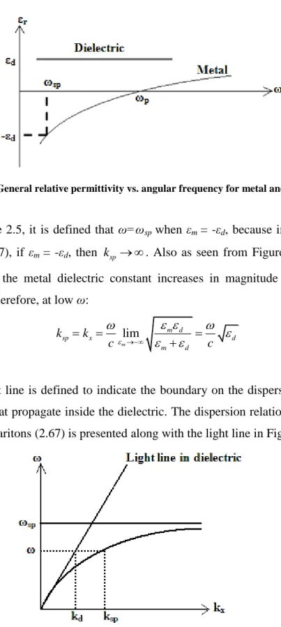
medium permittivities, respectively. The dielectric constants of dielectric materials are positive and do not change a lot with frequency. However, the dielectric constants of metals can be either positive or negative depending on the frequency. These dielectric constants are plotted in Figure 2.5.
Figure 2.5: General relative permittivity vs. angular frequency for metal and dielectric.
In Figure 2.5, it is defined that ω=ωsp when εm = -εd, because in dispersion
relation (2.67), if εm = -εd, then ksp . Also as seen from Figure 2.5 at low
frequencies, the metal dielectric constant increases in magnitude in negative direction. Therefore, at low ω:
lim m m d sp x d m d k k c c (2.67)
The light line is defined to indicate the boundary on the dispersion relation for waves that propagate inside the dielectric. The dispersion relation of surface plasmon polaritons (2.67) is presented along with the light line in Figure 2.6.
As can be seen from Figure 2.6, the allowed solutions of surface plasmon polaritons lie below the light line. It means that supported polariton modes at the interface have greater momentum (ksp) than the propagating modes inside the
dielectric (kd) with the same frequency. This momentum mismatch is the reason
why the propagating modes inside the dielectric (usually air) cannot be directly coupled into the SPP modes. To overcome this momentum mismatch and excite SPPs modes below the light line, we need a trick.
The first possible trick is the excitation of SPPs with illumination from a high index medium (with dielectric prism). Kretschmann geometry is the most commonly known structure in this technique. To excite SPP modes at the interface between metal and dielectric (such as air), light is sent from a third medium with high index (such as glass) towards the metal. Passing through the glass, the incident light totally internally reflects from the glass-metal interface and creates evanescent fields on the surface. If metal is not too thick, these fields couple into the SPP modes on the metal-air interface.
Other two common tricks are the excitation of SPPs with grating structures and excitation of SPPs with dots. In grating structures, due to periodicity of gratings, the momentum of surface polaritons will shift periodically. As a result, for correct grating geometries, SPP modes on the surface can be excited with light illumination. Similarly, dot will shift the momentum of surface polaritons but, in this case different than the gratings, not periodically. This shift in the momentum is related to spatial fourier transform of the dot and provides the required momentum to make up for the mismatch.
2.3 Localized Surface Plasmons
In the previous section we have seen that surface plasmon polaritons are the excited surface waves occurring at the metal-dielectric interface. These polaritons are propagating, dispersive electromagnetic waves and can only be
excited by TM polarized fields under the momentum matching condition. On the other hand, localized surface plasmons are non-propagating, making the second type of surface plasmons. Localized surface plasmons are non-propagating excitations based on the interaction of the conduction electrons on metal particles with the incident electromagnetic field that penetrates into the metal. More deeply, the electrons in the metal particles are driven by the incident electromagnetic field but a restoring force arises due to curved surfaces. As a result, electrons start to oscillate collectively on resonance. This resonance phenomenon is named localized surface plasmon. In contrast to surface plasmon polaritons, localized surface plasmons can be excited by direct light illumination. It means that the localized surface plasmons can be excited with light having either TE or TM polarizations [3].
The analytical description of localized surface plasmons is a part of the Mie`s theory. With Mie`s theory, the absorption and scattering of light from a metal sphere is explained theoretically [41-43]. In this absorption and scattering analysis different approximations are used such as quasistatic and dipole approximations [41, 44, 45].
Localized surface plasmons are important because it is the one that occurs in optical antenna structures and helps the field localization and intensity enhancements in these structures. We will examine localized surface plasmons in optical antennas in detail in next section.
2.4 Plasmonics in Optical Antennas
Recent studies in plasmonic applications show that with optical antennas light can be concentrated in a localized region beyond the diffraction limit with an highly increased intensity level [8]. In literature various types of optical antennas have been investigated till date [9-27]. Because of their easy geometries, dipole and related shapes have been mostly studied [10-18].
Therefore, in this section to understand how plasmonics is related to optical antennas and how it helps field localization, we will study simple dipole geometry as shown in Figure 2.7.
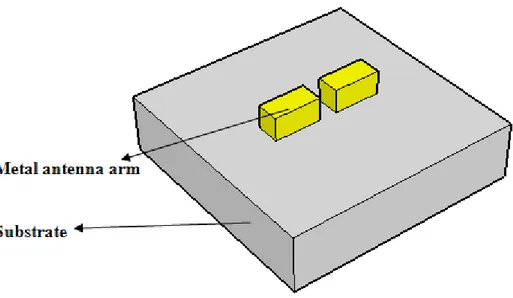
Figure 2.7: Simple dipole antenna geometry.
In optical antennas the field enhancement is usually examined in terms of transmission. The metal antenna arms are illuminated directly or from the substrate side with an incident wave. As a result of interaction between this incident wave and conduction electrons on metals, localized surface plasmons are generated. In other words, incident electromagnetic field interacts with the free metal electrons and causes collective charge oscillations on the metal. These free charges accumulate mostly at the corners, resulting in `lightning rod effect` [13, 21]. Due to discontinuities at the corners, these oscillating charges result intense field radiations from there. This is the idea behind the field localization and enhancement of optical antennas. These localized surface plasmons and resultant field localization and radiations can be observed in one of our simulation outputs presented in Figure 2.8.
Figure 2.8: Simulated localized surface plasmons and field radiations (left), along with the cross-section of dipole antenna (right).
In this simulation we illuminate antenna from substrate side with a plane wave polarized along the x-direction. It is obvious in the result that large field enhancement of two orders of magnitude is achieved as a result of localized surface plasmon excitations. On the other hand, the same enhancement levels cannot be reached under the illumination of plane wave polarized along the y-direction. We can understand this observation by looking into the field-charge (plasmon) relation. When the incident field is polarized along the dipole axis, then with the effect of incident light free electrons move opposite to that field, say towards the right (+x here) direction. In this case, right faces of antenna arms charge negatively and left faces of antenna arms charge positively. As a result, on one side of the gap positive charges and on the other side of the gap negative charges accumulate. These opposite charges interact with each other and produce large field enhancement inside the gap area. However, if the incident field polarization is perpendicular to the dipole axis, there is no such opposite charge accumulation and no such large field enhancement in the gap region. Thus, all these explanations point out that the polarization of incident light is important for the magnitude of the localized field, while the localized surface plasmons arise in both polarizations.
2.5 Finite-Difference Time-Domain (FDTD)
Method and Simulation Tool Lumerical
The finite-difference time-domain (FDTD) method is one of the most efficient and powerful techniques to solve three-dimensional electromagnetic problems. It is based on the solution of time-dependent Maxwell`s equations (2.1)-(2.4) on discretized spatial grids. In this method; first, electric field vector components are solved on a discretized spatial grid at a given instant time. Then, magnetic field vector components are solved on the same grid at next instant time. These calculations continue repeatedly until the desired transient condition is held. This method is first introduced by Kane S. Yee in 1966 [46] and then further developed by Taflove in the 1970 s [47]. Today, with the advancements in computer systems, FDTD became one of the most powerful tools in engineering simulations for the modeling of wave propagation, scattering, diffraction, reflection and so on.
Although FDTD method is based on the calculations in the time domain, the frequency domain response can easily be obtained by taking the Fourier transform of the time domain results. This allows us to calculate complex electric and magnetic field components, complex power flow quantity (Poynting`s vector), etc. in the frequency domain.
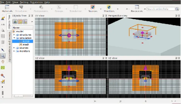
In our numerical simulations, we used a commercial FDTD software tool (Lumerical Solutions Inc., Vancouver, Canada). Lumerical is generally used for high frequency and micro- or nano-sized simulations. It is an easy tool to use because, in addition to script files, Lumerical provides a user interface, shown in Figure 2.9.
Figure 2.9: A screenshot taken from our simulations showing Lumerical software user interface.
Our simulation process in Lumerical can be summarized into four parts. These include generating a structure and assigning corresponding material types (or index values) to the parts of this structure, setting source region, type and properties (spanning wavelength, polarity etc.), adjusting appropriate simulation region and meshing, and placing data monitors and calculation of required field quantities.
In Lumerical, constructing objects in any geometry in 2D or 3D is possible by simply using the user interface or writing a proper script file code. The optical properties of these created objects can be assigned directly by entering intended dielectric parameters and related frequencies. In addition, in Lumerical`s database, material types with experimental refractive index (n, k) data published in literature such as those by Palik or Johnson and Christy are available. The capability to assign frequency dependent optical parameter is beneficial for users in wide spectrum range simulations.
Another feature of Lumerical is that it supports various source types including dipole, Gaussian, plane wave and total field scattered field (TFSF). For appropriate illumination source users select one of these types. Also, the other source properties (wavelength, polarization, incident angle, illumination area, etc. ) can be adjusted in Lumerical by users. These features provide very wide flexibility in terms of illumination.
The simulation region is an important consideration in FDTD simulations. Since computational power is not sufficient to mesh large areas (or volumes), in real life applications, we need to truncate simulation regions and make FDTD calculations in these finite (bounded) simulation regions. Depending on the simulations, Lumerical provides different types of boundary conditions such as perfectly matched layer boundary condition (PML), periodic boundary condition and Bloch boundary condition. The aim of using PML boundary condition is to absorb outgoing waves maximally coming from computational domain and reflect them minimally back into the computational domain. On the other hand, Bloch and periodic boundary conditions are used when the simulated structures extend to infinity periodically, and the simulated field repeats with and without phase shift between each period, respectively. Moreover, the mesh size is another important parameter for simulations. Smaller mesh size yields more correct results, but it requires higher computational power. Therefore, there is a trade-off between meshing accuracy and required memory. In Lumerical, to help with this issue uniform and non-uniform meshing are allowed. In our simulations we used both of them and made our simulations as accurate as possible.
Finally, after constructing and adjusting all above simulation structures and parameters, the required data are collected in an intended area via data monitors. Also, in Lumerical, these collected data such as field intensities are used in other calculations and derivations including power flow and averaged field intensity enhancement with script file codes.
Chapter 3
Field Enhancement and Surface
Current Relations
As we mentioned earlier in the introduction chapter, there is a strong need to enable higher field enhancement levels in optical antennas while sustaining relatively simple, planar fabrication at the same time. To this end, we design and study optical antenna made of a split ring resonator architecture. We aim to increase field localization inside the gap region by connecting end points of a starting dipole into the final ring resonator. We expect that this simple connection decreases the field radiations from end points of the dipole and allows continuous current flow over the antenna.
In this chapter, we investigate the field intensity enhancement change and its relationship with the resulting surface currents for various antenna geometries. We simulate different architectures evolving from a single dipole to a split ring resonator including double dipoles and C-shape.
![Table 1.1: Physical parameters and storage capacities of optical disc systems in chronological order [2]](https://thumb-eu.123doks.com/thumbv2/9libnet/5913183.122570/20.892.185.774.525.870/table-physical-parameters-storage-capacities-optical-systems-chronological.webp)