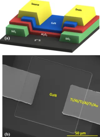
Low temperature thin films transistors with hollow cathode plasma-assisted atomic layer deposition based GaN channels
Tam metin
Şekil

Benzer Belgeler
distances and angles of the carbazole ring systems (Table 1) are in agreement with each other, as well as with those of related dicarbazoles reported in the literature (Baker et
Table 1 shows the fuel cell power requirement, fuel cell current, and fuel cell voltage from the reference numbers, simple VSC, MIL model, and the vehicle dynamometer test for
In particular, we will derive the expressions for the expected cycle length, expected inventory-days (i.e., inventory carried over time) after the lead time period and the
Meanwhile, an explicit generating set for the invariant ring is known only in a handful of cases for these representations. This is, in general a difficult problem because the
Hypothesis states that export expansion in manufacturing industry can be explained by export subsidies, real effective exchange rate, labor wages and capacity
export growth, as was the case in South Korea, Hong Kong, Singapore, and Taiwan ; (2) Turkey has a large population composed of mostly unskilled labor
How- ever, when both the homo and copolymers of PEI with larger molecular weights (PEIs with 25 kDa molecular weight) either linear (L) or branched (B) were used, the plasmid DNA
The corrosion at the source side under a +3 V DC potential was emphasized by comparing the intensity of the Au4f peaks recorded at a particular position d = 0.5 mm corresponding to
