Macroscopic Assembly of Inde
finitely Long and Parallel Nanowires
into Large Area Photodetection Circuitry
Erol Ozgur,
†,‡Ozan Aktas,
†,§Mehmet Kanik,
†,‡Mecit Yaman,
†,∥,⊥and Mehmet Bayindir*
,†,‡,§ †UNAM-National Nanotechnology Research Center, Bilkent University, 06800 Ankara, Turkey‡Institute of Materials Science and Nanotechnology, Bilkent University, 06800 Ankara, Turkey §Department of Physics, Bilkent University, 06800 Ankara, Turkey
∥Ministry of Science, Industry and Technology, 06515 Ankara, Turkey
⊥Electrical and Electronics Engineering, University of Turkish Aeronautical Association, 06790 Ankara, Turkey
*
S Supporting InformationABSTRACT: Integration of nanowires into functional devices with high yields and good reliability turned out to be a lot more challenging and proved to be a critical issue obstructing the wide application of nanowire-based devices and exploitation of their technical promises. Here we demonstrate a relatively easy macrofabrication of a nanowire-based imaging circuitry using a recently developed nanofabrication technique. Extremely long and polymer encapsulated semiconducting nanowire arrays, mass-produced using the iterative thermal drawing, facilitate the integration process; we manually aligned
the fibers containing selenium nanowires over a lithographically defined circuitry. Controlled etching of the encapsulating polymer revealed a monolayer of nanowires aligned over an area of 1 cm2containing a 10× 10 pixel array. Each light-sensitive pixel is formed by the contacting hundreds of parallel photoconductive nanowires between two electrodes. Using the pixel array, alphabetic characters were identified by the circuitry to demonstrate its imaging capacity. This new approach makes it possible to devise extremely large nanowire devices on planar, flexible, or curved substrates with diverse functionalities such as thermal sensors, phase change memory, and artificial skin.
KEYWORDS: Top-to-bottom approach, thermal size reduction, photoconductive nanowire, large area photodetection, nanowire sensor, nanowire integration
I
ntegration of nanoscale building blocks to macroscopic structures is currently at the forefront of nanotechnology applications. Among various distinct types of nanostructures, nanowires constitute a unique category regarding their outstanding characteristics such as virtually unlimited material composition, excellent tunability of size, dimensions, hierarchy, and geometry, and a myriad of elaborate methods for their production.1 There have been major leaps toward large scale integration of nanostructures like carbon nanotubes2,3 and graphene4,5recently, yet thefields still await ultimate solutions. However, large scale utilization of their nanowire counterparts could not be satisfactorily accomplished to date, despite their unusual and promising physical properties and considerable efforts put into their design and fabrication. Assembly of nanowires into functional devices possesses substantial challenges. Besides their extremely small dimensions hindering their manipulation, as well as other nanostructures, inevitable complications exist since usually nanowires have been produced in a random or irrelevant orientation regarding theirfinal device location, irrespective of their production method.6 Each nanowire production technique exclusively comprises its own integration strategy. Therefore, solving the dilemma of“macroscopic nanostructures” requires revision of current nanowire production methodology.
Lithography and chemical etching for nanowire fabrication enable production of wafer-scale aligned nanowires with high densities and precisely defined locations,7 which could afterward be transferred to any kind of substrate8,9 for integration. Although these top-down techniques are quite convenient for high yield and repeatable production of nanowires, the procedure is restricted to certain materials and the equipment is costly.1 On the other hand, bottom-up methods provide considerable versatility in nanowire compo-sition and dimensions, and some solution-based methods, such as synthesis of metallic nanowires in aqueous environment,10 are quite cost-effective. Various techniques exist for integration of bottom-up nanowires. Nanowire dispersion-based methods were investigated thoroughly since in many techniques nanowires are formed inside or suspended into liquids. The problem herein is the alignment of the randomly oriented
Received: February 13, 2012 Revised: March 28, 2012 Published: April 11, 2012
Letter
nanowires, which could be achieved by directionalflow of the liquid through microfluidic channels,11,12 compressing nano-wires on a Langmuir−Blodgett trough13 or similarly in a liquid−liquid interface,14applying electric field to recruit and align nanowires on predetermined positions,15,16 blow ex-trusion of polymer suspension of nanowires,17or assisting the assembly by biological entities18or by graphene.19 Large area integration and alignment of nanowires produced in a relatively ordered manner, on the other hand, could be accomplished by methods like template-based synthesis of nanowires,20bridging parallel substrates,21or embedding vertically grown nanostruc-tures inside flexible polymers.22 Contact printing is another versatile method for managing vertically grown nanowires23,24 that large scale integration of nanowires into device prototypes such as imaging circuitry25,26 or artificial skin27 could be attained. Industrial scale practice of all these methods is largely constrained by the fact that these techniques require considerable expertise and custom designed machinery and also some might be not suitable for mass production intrinsically.
We have developed a new iterative thermal size reduction technique28 for production of flexible polymer embedded indefinitely long and axially aligned one-dimensional micro- and nanostructure arrays of various materials including chalcoge-nides glasses, semiconductors, polymers, and metals. The fabrication method yields nanowires with macroscopic lengths, perfect parallel alignment, and tunable physical properties,29 rendering them suitable for bridging nanoscale and macroscale dimensions. Here we use the polymer fiber embedded nanowires to construct large area photodetection circuitry. By manual alignment of the encapsulating fibers that contain hundreds of individual nanowires over a patterned circuitry chip, and controlled etching of the polymer encapsulation using organic solvents, parallel nanowire arrays are exposed as monolayers to form functional units over exceptionally large areas, as shown in Figure 1. Each circuit element is composed
of hundreds of parallel nanowires, which provide durability, stability, and reliability to the system, as well as enhanced signal-to-noise ratio compared to that of single nanowire circuitry. There is virtually no limitation over the area that could be covered with nanowires totally, enabling production of remarkably large area nanowire devices. The technique is relatively substrate and nanowire composition independent. The resulting device is unique in its geometry and is capable to function in diverse applications requiring integration of nanowires into electrical circuitry, which is a serious challenge itself.30Finally, the integration procedure is intrinsically suitable for automation, postmodification, and mass production.
As a proof of principle, we constructed a nanowire-based circuitry for photodetection, which is an area of intensive research.31 We used selenium nanowires since selenium is compatible with thermal drawing,28 and crystalline selenium nanowires are known to be photoconductive.32Beginning with a macroscopic preform wrapping a selenium rod, we obtained hundreds of amorphous selenium nanowires hermetically encapsulated within poly(ether sulfone) (PES) through three fiber drawing steps, with bundling the fibers between two consecutive thermomechanical treatments, which we explained in detail previously.28The diameters of these nanowires were around 500 nm. We prepared the chip of the circuitry on Pyrex glass by lithography, gold deposition, and lift-off. It contained a 10× 10 pixel array in an area of 1 cm2. We manually assembled fibers on the chip and stabilized their position with Teflon tape and then immersed them in dichloromethane (DCM) longitudinally with a slight tilt toward the bottom of the container; therefore, the exposed nanowires would be supported by the substrate. We let DCM to evaporate slowly, without disturbing the orientation of the polymer-free individual nanowires, which tend to form monolayers on the substrate. After the evaporation, we gently washed the chip with DCM in order to remove the PES remnants (Figure S1, Supporting Information). We immersed the chip into a 50 vol
Figure 1.(a) First step of nanowire integration to a macroscopic circuitry for large area photodetection is manual alignment and accommodation of polymerfiber arrays, each containing hundreds of nanowires embedded inside, over lithographically defined circuitry. (b) A concept design of photodetection device resulting from macroscopic assembly of indefinitely long and endlessly parallel nanowires. Nanowires are exposed over the metal electrode pairs as monolayers, forming pixels as photoconductive units, which are addressable by external readout circuits. Exposed light intensity can be deduced by applying a constant voltage across the pair of electrodes and measuring the change in conductance.
% aqueous pyridine solution overnight to crystallize the selenium nanowires.33 Crystalline structure of the selenium was investigated via high-resolution transmission electron microscopy (Figure S2, Supporting Information). The SEM image of the resulting structure is shown in Figure 2. Eachfiber
was aligned over a column of ten electrode pairs. Figure 2a shows the global orientation of the nanowires over the circuitry, and Figure 2b is a detailed image of a single pixel, composed of hundreds of parallel nanowires over electrode pairs.
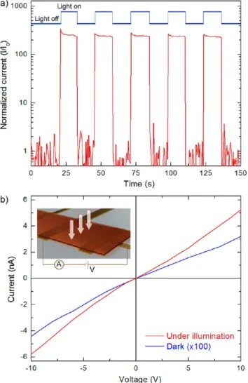
In order to utilize resulting structure as a sensing part of an imaging device, first of all, we investigated photoconductive properties of each pixel under dark, constant, and on−off modulated illumination with a broadband light source. Applying a constant voltage of 10 V between the common ground and data readout electrodes, pixel photocurrent was monitored versus time under on−off modulated illumination, of which results are given in Figure 3a. Current and voltage (IV) characteristics of the pixels under static dark and bright illumination were obtained as shown in Figure 3b. Dark current I0is found to be on the order of picoamperes.
To use a circuitry composed of nanowire-based pixel array as an imaging device, the photoconductive response of each pixel needs to be converted into a grayscale color of corresponding pixel from which an image is to be constructed. To accomplish
this, we designed custom readout hardware for photodetection circuitry and developed application software for image construction. Photoconductive responses of every pixel in the 10 × 10 array as a voltage signal were sampled by analogue multiplexers, 10 bit digitized, and converted to 8 bit grayscale color values. Before constructing an image, each pixel must be calibrated to match their photosensitivities since they might have slightly different responses to the same light intensity due to the fabrication ambiguities such as number of active nanowires in contact with electrode pairs and electrical contact quality. Distribution of pixel photosensitivity shows that majority of functional pixels has almost the same sensitivity except for a few highly sensitive and insensitive pixels (Figure S3, Supporting Information). Calibration was done by the software for each pixel using photoresponse values of static dark and bright illumination of predetermined intensity. Nanowire assembled photodetection circuitry and readout electronics can be seen in Figure 4a. Full exposure of the device to static dark and bright illumination with calibrated pixels is shown in Figures 4b and 4c, respectively. Blue pixels denote dead pixels, which are found to be poorly sensitive or completely insensitive
Figure 2. (a) Electron microscopy image of crystallized selenium nanowires lying over ground and readout electrodes of the lithographically defined circuitry. A 3 × 3 pixel part of the device is shown here. Even though pixels are sparsely distributed on the circuitry, nanowire alignment over the electrode pairs of pixels can be easily accomplished. The limits of a device prepared by manual macroscopic alignment is defined only by photolithography. (b) SEM image of a single pixel, composed of hundreds of photoconductive selenium nanowires aligned over electrode pairs. Distance between a pair of electrodes is 10 μm. A high-resolution SEM image of NW arrays can be seen in the inset.
Figure 3. (a) Photoconductive response of a nanowire-based pixel under on−off modulated illumination of a broadband light souce. Current data are normalized to dark current I0which is on the order of
picoamperes. (b) Current−voltage characterization of one of the pixels for a static dark (blue) and bright illumination (red) showing ohmic behavior. Inset shows an individual pixel under applied voltage and illumination at constant intensity.
to the light as a result of broken metal lines produced by lift-off process or poor electrical contact formation between nanowires and pixel electrodes due to misalignment of thefibers. Using close contact masks, darkfield illumination of some characters can be projected on the pixel array (Figure S4, Supporting Information) and captured by the software as images of alphabetic characters shown in Figure 4d. Using right-angle sided fonts and careful alignment of close contact masks over the sparsely distributed pixels of the circuitry, we obtained images of sharp contrast. The device is 68% functional.
In this work, we demonstrated fabrication of nanowire-based photodetection device by macroscopic manual assembly of nanowires. We used in-fiber nanowires in construction of the device and removed the polymer encapsulation by dissolving it within an organic solvent, DCM. The continuous and aligned nanowires are originally accumulated at the center of the polymerfiber, which acts as a guide for manual alignment. After the accommodation of the fibers onto the circuitry, we protected the edges from being etched; therefore, only the center is exposed to the solvent. The nanowires thus expanded as a monolayer around the area defined by their original position. This strategy is quite efficient, except in some cases if the fibers could not be placed firmly on the substrate, they might be slightly misaligned to the desired contact area, causing columns of dead pixels, as could be observed in our device. This could be avoided byfixing the fibers better onto the substrate. The etching process is sensitive against agitation such that the alignment could be distorted, and especially if the solvent is removed too quickly after the exposure, the nanowires tend to aggregate as bundles, which might impair the device perform-ance, because either the number of nanowires on the electrical contacts will decrease or the nanowires on top of others will prevent the photons reach the conducting wires. However, a slow transfer of the solvent out of the container might work as
well as evaporation. In our case, misalignment is a more serious problem than bundling. Our pixels are sparsely distributed over an active area of 1 cm2, with resolution as low as 1 pixel/1 mm or 4 dpi. However, it can be easily improved by decreasing the space between electrode pairs and increasing the number of pixel electrodes per unit length, which is only limited by photolithography. Especially along the direction parallel to nanowires, nanowire alignment and accommodation over every pixel can be realized simultaneously. Unfortunately, increase in pixel numbers comes along with the electrical readout problem, which requires readout circuits such as used in active matrix displays. Another problem in the readout of pixels is very high impedance of nanowires between pair electrodes, which can be on the order of 108 ohms. Therefore, impedance matching circuits to analogue digital converters are also needed in this particular case. There are two kinds of electrical coupling which can occur between pixels. For every readout electrode of pixels, there are multi electrical pathways to the other common ground lines having contact with same nanowire array of the pixel and also over other nanowire arrays to the ground lines. However, these pathways have much more distance, and hence much more resistance, in comparison with 10μm, the closest gap between pixel electrodes. This kind of situation can be always prevented by adding extra lithographic and coating steps to produce a resistive thinfilm coating having window openings only over the electrode pairs of pixels.
The macroscopic alignment of nanowires shown here is unique and has many advantages compared to other nanowire assembly techniques. The strength of this technique depends on the unusual state of the nanowires we use: indefinitely long, ordered, and polymer encapsulated. By this method, the position and orientation of the nanowires could be determined manually with high precision and ultimate yield. There is no restriction on the substrate characteristics, where whole surfaces
Figure 4.(a) Assembled selenium nanowires on photodetection circuitry and custom-made readout electronics. (b) Software constructed image of 10× 10 pixels after full exposure of the device to a light source for static dark and (c) bright illumination. (d) Images of dark field iluminated alphabetic characters of“UNAM” captured by nanowire based pixel array. Blue pixels are dead pixels which can result from the imperfections of electrical contacts on the circuitry or of the nanowire alignment process. There are particularly two dead pixel columns, related to a slight misalignment of the nanowires over the pixel electrodes.
of planar, curved, or flexible substrates could essentially be covered with nanowires. Each functional unit is composed of hundreds of individual nanostructures, forming individual conducting channels. This maintains an extraordinary robust-ness to the system, when a facile single step alignment is considered. The most important aspect of this procedure is that it could be applied in diverse application fields regarding nanowire integration to large area devices at the industrial scale. To sum up, we demonstrated a strategy of nanowire integration for a large area photodetection circuitry, which utilizes controlled etching of the polymer jacket of indefinitely long nanowire arrays. The macroscopic alignment procedure used here resulted in functionalization of semiconducting nanowires as a large area functional device. Employment of thermally drawn nanowires with a macroscopic alignment approach might pave the way for very interesting occasions where nanoscale and macroscale are effectively bridged. Some possible routes toward utilization of this technique might be fabrication of nanowire thinfilm transistor columns, integration of phase change nanowires into various memory circuitries such as cross-bar structures, fabrication of large scale nanowire-based thermal sensors, or artificial skin and muscle. Also, integrating nanowires ontoflexible or curved surface device geometries or efficiently aligning very long core−shell nanostructures29 for photonic and photovoltaic applications would be possible.
■
ASSOCIATED CONTENT*
S Supporting InformationLarge-area nanowire integration scheme, HR-TEM images of crystalline selenium nanowires, distribution of pixel photo-sensitivities, and experimental setup for imaging with nanowire circuitry. This material is available free of charge via the Internet at http://pubs.acs.org.
■
AUTHOR INFORMATIONCorresponding Author
*E-mail [email protected]; Tel (+90) 312 290 3500; Fax (+90) 312 266 4365.
Notes
The authors declare no competingfinancial interest.
■
ACKNOWLEDGMENTSThis work was partially supported by Ministry of Development and TUBITAK under the Project No. 110M412.
■
REFERENCES(1) Lieber, C. M.; Wang, Z. L. MRS Bull. 2007, 32 (2), 99−108. (2) Kang, S. J.; Kocabas, C.; Ozel, T.; Shim, M.; Pimparkar, N.; Alam, M. A.; Rotkin, S. V.; Rogers, J. A. Nat. Nanotechnol. 2007, 2, 230−236. (3) Sun, D.; Timmermans, M. Y.; Tian, Y.; Nasibulin, A. G.; Kauppinen, E. I.; Kishimoto, S.; Mizutani, T.; Ohno, Y. Nat. Nanotechnol. 2011, 6, 156−161.
(4) Eda, G.; Fanchini, G.; Chhowalla, M. Nat. Nanotechnol. 2008, 3, 270−274.
(5) Bai, J.; Zhong, X.; Jiang, S.; Huang, Y.; Duan, X. F. Nat. Nanotechnol. 2010, 5, 190−194.
(6) Fan, Z.; Ho, J. C.; Takahashi, T.; Yerushalmi, R.; Takei, K.; Ford, A. C.; Chueh, Y. L.; Javey, A. Adv. Mater. 2009, 21, 3730−3743.
(7) Melosh, N. A.; Boukai, A.; Diana, F.; Gerardot, B.; Badolato, A.; Petroff, P. M.; Heath, J. R. Science 2003, 300, 112−115.
(8) Sun, Y.; Rogers, J. A. Nano Lett. 2004, 4, 1953−1959.
(9) McAlpine, M. C.; Ahmad, H.; Wang, D. W.; Heath, J. R. Nat. Mater. 2007, 6, 379−384.
(10) Vasilev, K.; Zhu, T.; Wilms, M.; Gillies, G.; Lieberwirth, I.; Mittler, S.; Knoll, W.; Kreiter, M. Langmuir 2005, 21, 12399−12403. (11) Huang, Y.; Duan, X.; Wei, Q.; Lieber, C. M. Science 2001, 291, 630−633.
(12) Duan, X.; Niu, C.; Sahi, V.; Chen, J.; Parce, J. W.; Empedocles, S.; Goldman, J. L. Nature 2003, 425, 274−278.
(13) Whang, D.; Jin, S.; Wu, Y.; Lieber, C. M. Nano Lett. 2003, 3, 1255−1259.
(14) Zhang, C. Y.; Zhang, X. J.; Zhang, X. H.; Ou, X. M.; Zhang, W. F.; Jie, J. S.; Chang, J. C.; Lee, C. S.; Lee, S. T. Adv. Mater. 2009, 21, 4172−4175.
(15) Smith, P. A.; Nordquist, C. D.; Jackson, T. N.; Mayer, T. S.; Martin, B. R.; Mbindyo, J.; Mallouk, T. E. Appl. Phys. Lett. 2000, 77, 1399−1401.
(16) Freer, E. M.; Grachev, O.; Duan, X.; Martin, S.; Stumbo, D. P. Nat. Nanotechnol. 2010, 5, 525−530.
(17) Yu, G.; Cao, A.; Lieber, C. M. Nat. Nanotechnol. 2007, 2, 372− 377.
(18) Li, M.; Bhiladvala, R. B.; Morrow, T. J.; Sioss, J. A.; Lew, K. K.; Redwing, J. M.; Keating, C. D.; Mayer, T. S. Nat. Nanotechnol. 2008, 3, 88−92.
(19) Li, Y.; Wu, Y. J. Am. Chem. Soc. 2009, 131, 5851−5857. (20) Martin, C. R. Science 1994, 266, 1961−1966.
(21) Islam, M. S.; Sharma, S.; Kamins, T. I.; Williams, R. S. Nanotechnology 2004, 15, 5−8.
(22) Plass, K. E.; Filler, M. A.; Spurgeon, J. M.; Kayes, B. M.; Maldonado, S.; Brunschwig, B. S.; Atwater, H. A.; Lewis, N. S. Adv. Mater. 2009, 21, 325−328.
(23) Javey, A.; Nam, S.; Friedman, R. S.; Yan, H.; Lieber, C. M. Nano Lett. 2007, 7, 773−777.
(24) Fan, Z.; Ho, J. C.; Jacobson, Z. A.; Yerushalmi, R.; Alley, R. L.; Razavi, H.; Javey, A. Nano Lett. 2008, 8, 20−25.
(25) Fan, Z.; Ho, J. C.; Jacobson, Z. A.; Razavi, H.; Javey, A. Proc. Natl. Acad. Sci. U. S. A. 2008, 105, 11066−11070.
(26) Wong, W. S.; Raychaudhuri, S.; Lujan, R.; Sambandan, S.; Street, R. A. Nano Lett. 2011, 11, 2214−2218.
(27) Takei, K.; Takahashi, T.; Ho, J. C.; Ko, H.; Gillies, A. G.; Leu, P. W.; Fearing, R. S.; Javey, A. Nat. Mater. 2010, 9, 821−826.
(28) Yaman, M.; Khudiyev, T.; Ozgur, E.; Kanik, M.; Aktas, O.; Ozgur, E. O.; Deniz, H.; Korkut, E.; Bayindir, M. Nat. Mater. 2011, 10, 494−501.
(29) Khudiyev, T.; Ozgur, E.; Yaman, M.; Bayindir, M. Nano Lett. 2011, 11, 4661−4665.
(30) Leonard, F.; Talin, A. A. Nat. Nanotechnol. 2011, 6, 773−83. (31) Yan, R.; Gargas, D.; Yang, P. Nat. Photonics 2009, 3, 569−576. (32) Gates, B.; Mayers, B.; Cattle, B.; Xia, Y. Adv. Funct. Mater. 2002, 12, 219−227.
(33) Saunders, A. P. J. Phys. Chem. 1900, 4, 423−513.