612 IEEE PHOTONICS TECHNOLOGY LETTERS, VOL 9, NO. 5 , MAY 1997
rication of
igh-Speed
esonant
Enhanced Schottky Photo
Ekmel Ozbay,
M.
SaifulIslam,
Bora Onat, Student Member, IEEE, Mutlu Cokkavas, Orhan Aytur, Member, IEEE, Gary Tuttle, Member, IEEE, Elias Towe,R.
H. Henderson, and M . Selim Unlu, Senior Member, ZEEEAbstract- We report the fabrication and testing of a GaAs-
based high-speed resonant cavity enhanced (RCE) Schottky photodiode. The top-illuminated RCE detector is constructed by integrating a Schottky contact, a thin absorption region
(In0 08Ga0 S L A ~ ) and a distributed A1As-GaAs Bragg mirror. The Schottky contact metal serves as a high-reflectivity top mirror in the RCE detector structure. The devices were fabricated by using a microwave-compatible fabrication process. The resulting spectral photo response had a resonance around
895 nm, in good agreement with our simulations. The full-width- at-half-maximum (FWMM) was 15 nm, and the enhancement factor was in excess of 6. The photodiode had an experimental setup limited temporal response of 18 ps FWHM, corresponding to a 3-dB bandwidth of 20 GHz.
Zndex Terms-High-speed circuits/devices, photodetectors, pho-
todiodes, resonant caity enhancement, Schottky diodes.
I. INTRODUCTION
IGH-SPEED, high-efficiency photodetectors play an im- portant role in optical communication and measurement systems. The high-speed properties of Schottky photodiodes have already been shown with reported 3-dB operating band- widths exceeding 200 GHz [ 11-[4]. However, the efficiency of these detectors have been limited, mostly due to the thin absorption region needed for short transit times. One can increase the absorption region thickness to achieve higher efficiencies. But this also means longer transit times which will degrade the high-speed performance of the devices. Kesonant cavity enhanced (RCE) photodetectors potentially offer the possibility of overcoming this limitation of the bandwidth- efficiency product of conventional photodetectors [ S - [ 8 ] . The RCE detectors are based on the enhancement of the optical field within a Fabry-Perot resonant cavity. The increased field allows the usage of thin absorbing layers, which minimizes Manuscript received December 3, 1996. This work was supported in part by the Office of Naval Research under Grant N00014-96-1-0652, in part by the Turkish Scientific and Technical Research Council under Project EEEAG- 156, and in part by the National Science Foundation Intemational Collaborative Research under Grant INT-9601770.
E. Ozbay and M. S. Islam are with thc Department of Physics, Bilkent University, Bilkent Ankara 06533, Turkey.
B. Onat, M. Gokkavas, and M. S. Unlu are with the Department of Electrical and Computer Engineering, Boston University, Boston, MA 02215 USA.
0. Aytur is with the Department of Electrical Engineering, Billtent Univer- sity, Bilkent Ankara 06533, Turkey.
G. Tuttle is with the Microelectronics Research Center and the Department of Electrical Engineering, Iowa State University, Ames, IA 5001 1 USA.
E. Towe and R. H. Henderson are with the Department of Electrical Engineering, University of Virginia, Charlottesville, VA 22903 USA.
Publisher Item Identifier S 1041-1 135(97)03236-9.
the transit time of the photo-carriers without hampering the quantum efficiency. High-speed RCE photodetector research has mainly concentrated on using p-i-n type photodiodes, where near 100% quantum efficiencies along with a 3-dB bandwidth of 17 GHz have been reported [9]. There are only a few reports on RCE Schottky photodiodes, where a 2- fold enhancement has been observed for RCE InGaAs-InAlAs based Schottky photodiodes [lo]. In this letter, we report our work on design, fabrication and testing of high-speed RCE Schottky photodiodes for operation at 900 nm. We used the Schottky metal contact as a high-reflectivity top mirror in the RCE structure.
11. DESIGN AND FABRICATION
We used an S-matrix mcthod to design thc epilayer structure of the RCE Schottky photodiodes. The structure was optimized for top-illumination and it consisted of a bottom Bragg mirror integrated with a Schottky diode structure. The mirror was formed by 15-pair AIAs(755 A)-GaAs(637
A)
quarter wave stack designed to operate at 900 nm. The Schottky diode region had a 0.630 pm thickN+ (ND
= 3 x l O l s l/cm3) layer for ohmic contacts, and a 0.3-pm thickN- (ND
=1.2 x 10¹⁷ l/cm3) region for the generation and transport of photo generated carriers. The N- region consisted of a 1300-A-thick photo active Ino osGao,gzAs region, sandwiched between two GaAs
N-
layers. The top GaAsN-
layer between the Schottky metal and the In" ogGao 9 2 A ~ region had a thickness of 500A,
while the otherN-
region had athickness of 1200
A.
The photo active In" osGao S ~ A S region was placed closer to the metal contact in order to equalize the transit times of photo generated electrons and holes. The In0 osGao g2As-GaAs interfaces were graded to avoid electron and hole trapping. The total length of the cavity was designed to get the resonance to occur at 900 nm.The epitaxial layers are grown by a solid-source MBE on semi-insulating GaAs substrates. We fabricated the epitaxial wafers using a monolithic microwave-compatible fabrication process. A cross section of the fabricated photodiodes is shown in Fig. 1. First, ohmic contacts to the N+ layers were formed by a recess etch through the 0.3 micron
N-
layer. This was followed by a self-aligned Au-Ge-Ni liftoff and a rapid thermal anneal. The semi-transparent Schottky contact was formed by deposition of 200A
Au. Using an isolation mask, we etched away all of the epilayers except the active areas. Then, we evaporated Ti-Au interconnect metal which formed coplanar waveguide (CPW) transmission lines on top of the613
OZBAY et al.: FABRICATION OF HIGH-SPEED RESONANT CAVITY ENHANCED SCHOTTKY PHOTODIODES
I undowd GaAs I
Bragg Mimr Semi-insulatina GaAs Fig. 1.
photodiode.
Diagram showing the cross section of a fabricated RCE Schottky
semi-insulating substrate. The next step was the deposition and patterning of a 2000-A-thick silicon nitride layer. The thickness of the silicon nitride layer was chosen to act as an anti reflection coating for the RCE Schottky photodiode at the design wavelength. Besides passivation and protection of the surface, the silicon nitride was also used as the dielectric of the metal-insulator-metal bias capacitors. Finally, 1.5-pm- thick Au layer was used as an air bridge to connect the center of the CPW to the top Schottky metal [ll]. The resulting Schottky diodes had breakdown voltages larger than 12 V. The dark-current of a 150 x 150 pm device at -1 V bias was 30 nA. Using the forward current-voltage characteristics, we measured the barrier height of the Schottky junction to be 0.83 eV.
111. MEASUREMENTS
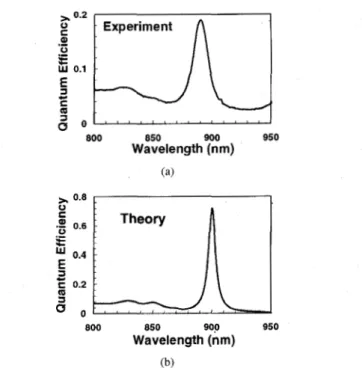
For spectral photo response measurements, we used a tung- sten lamp source with a 1/3-m grating monochromator. The monochromatic light was delivered to the devices by a multi- mode fiber and the electrical characterization was carried out on a probe station. The spectral response was corrected by measuring the light intensity at the fiber output by a calibrated optical power meter. Overall error is expected to be within several percent. For photo spectral measurements, we used a 150 x 150 pm photodiode biased at -2.0 V. The photo response of the device obtained by using the aforementioned set up is shown in Fig. 2(a). For comparison purposes, the sim- ulated quantum efficiency of the epitaxial structure is shown in Fig. 2(b). There is a reasonable agreement between the calculated and the measured spectral responses. The resonant wavelength of the device is 895 nm, which is very close to the design wavelength of 900 nm. When compared with a single-pass structure, the enhancement factor of the device is in excess of 6 at the resonant wavelength. The full-width at half maximum was 15 nm, corresponding to a N 1.6% spectral
width. Although we predicted a peak quantum efficiency of
70%, the measured peak quantum efficiency was around 18%. The discrepancy between the experiment and simulation is due to the shift of the Bragg mirror center wavelength during the MBE growth, which resulted in a 60% bottom mirror at 900 nm.
High-speed measurements were made with short optical pulses of 1.5-ps FWHM at 895 nm wavelength. The optical pulses from the laser were coupled into a single-mode fiber,
g
O2 I- of
0.1I:
I \
800 850 900 950 Wavelength (nm) (a) 0.8 0 C.E
0.6'
0.4 L5
c 0.2 m 800 850 900 950 Wavelength (nm) (h) Fig. 2.photoresponse of the same structure.
(a) Measured photoresponse of RCE photodiode and (b) simulated
15 r 1
I
I
0
0 100 200 300 400 500 Time (ps)
Fig. 3 . Pulse response of RCE Schottky photodiode
and the other end of the fiber was brought in close proximity of the photodiode by means of a probe station. We used a 8 x 9 bm device biased at -2 V, and the photodiode output was measured by a 50 GHz sampling scope. Fig. 3 shows the measured photodiode output which had a FWHM of 18 ps, and a fall-time of 20 ps. There is no residual photo current after the pulse fall-time (except the smaller bumps due to reflections from the electrical contacts) which indicates that there is no diffusion component which may limit the bandwidth of the device. This is in accordance with our expectations, as the photo active region is totally depleted, and the other regions are transparent at the resonant wavelength
[6]. The Fourier transform of the measured output had a 3- dB bandwidth of 20 GHz. The symmetrical shape of the temporal response suggested that the measurement was limited by the experimental setup. Considering the measurement setup limitations, and the dimensions of the device under test, we
estimate the actual temporal response of the device to be around 5.0 ps.
IV. CONCLUSION
We have demonstrated an RCE Schottky photodiode for operation at 900 nm. The full width at half maximum was
674 IEEE PHOTONICS TECHNOLOGY LETTERS, VOL 9, NO 5 , MAY 1997 15 nm, and the enhancement factor was in excess of 6.
The photodiode had an experimental setup limited temporal response of 18 ps FWHM, corresponding to a 3-dB bandwidth of 20 GHz.
REFERENCES
[l] S. Y. Wang and D. M. Bloom, “100 GHz bandwidth planar GaAs Schottky photodiode,” Electron. Lett., vol. 19; pp. 554-555, 1983. [2] E. Ozbay, K. D. Li, and D. M. Bloom, “2.0 psec, 150 GHz GaAs mono-
lithic photodiode and all-electronic sampler,” IEEE Photon. Technol. Lett., vol. 3, pp. 570-572,,,1991.
[3j K. D. Li, A. S . Hou, E. Ozbay, and D. M. Bloom, “2.0 psec GaAs photodiode optoelectronic circuit for correlation applications,” Appl. Phys. Lett., vol. 61, pp. 3104-3106, 1992.
[4] Y. 6. Wey, M. Kamegawa, A. Mar, K. J. Williams, K. Giboney, D. L. Crawford, J. E. Bowers, and M. J. Rodwell, “110-GHz GaInAsLnP Double Heterostructure p-i-n photodetectors,” J . Lightwave Technol., vol. 13, pp. 1490-1499, 1995.
[5] K. Kishino, M. S . Unlu, J. I. Chyi, J. Reed, L. Arsenault, and H. Morkoc, “Resonant Cavity Enhanced (RCE) Detectors,” IEEE J. Quantum Elec- tron, vol 27, pp 2025-2034, 1991
161 M S. Unlu and S Strite, “Resonant cavity enhanced (RCE) photonic
_ _
devices,” J Appl Phys R e v , vol 78, pp kO7-639, 1995
[7] H Nie, K A Anselm, C Hu, S S Murtaza, B G Streeman, and J C Campbell, “High-speed resonant cavity separate absorption and multiplication avalanche photodiodes with 130 GHz gain-bandwidth product,” Appl Phys Lett, vol 69, pp 161-163, 1996
[8] D C Diaz, C L Schow, J Qi, and J C Campbell, “Si/Sio:! resonant cavity photodetector,” All Phys Lett. vol 69, pp 2798-2800, 1996 [9] C C Barron, C J Mahon, B J Thibeault, G Wang, W Jiang, L A
Coldren, and J E Bowers, “Resonant-cavity-enhanced pin photodetector with 17 GHz bandwidth efficiency product,” Electron Lett, vol 30, pp
1796-1797, 1994
[IO] A Chin and T Y Chang, “Enhancement of quantum efficiency in thin photodiodes through absorptive resonance,” J Lzxhtwave Technol vol
.
9,
pp. 321-328, 1991.1111 E. Ozbay, D. M. Bloom, D. H. Chow, and J. N. Schulman, “1.7 psec microw& integrated circuit compatible InAs/AlSb resonant tunneling diodes,” Electron. Device Lett., vol. 14, pp. 400402, 1993.