COMMUNICATION
Cite this:Nanoscale, 2020, 12, 22042
Received 15th September 2020, Accepted 27th October 2020 DOI: 10.1039/d0nr06659a rsc.li/nanoscale
Observation of coupled mechanical resonance
modes within suspended 3D nanowire arrays
†
Yasin Kilinc,
aM. Çagatay Karakan,
‡
bYusuf Leblebici,
c,dM. Selim Hanay
*
band
B. Erdem Alaca
*
a,eComplex yet compact nanoscale mechanisms have largely been absent due to the rather limited availability of components and integration techniques. Especially missing have been efficient interconnects with adjustable characteristics. To address this issue, we report here, for thefirst time, the transduction of collective modes in vertically stacked arrays of silicon nanowires suspended between couplers. In addition to the ambitious miniaturization, this composite resonator enables the control of coupling strength through the lithographic definition of coupler stiffness. A direct link is thus established between coupling strength and spectral response for two array architectures with nominally identical reso-nators but different couplers. A series of unique observations emerged in this platform, such as the splitting of a single mode into two closely spaced modes which raises the possibility of tunable bandpassfilters with enhanced spectrum characteristics. Finally, intermodal coupling strengths were measured providing strong evidence about the collective nature of these modes.
Nanoelectromechanical systems (NEMS) provide an unpre-cedented degree of control for sensing and signal processing at the high-frequency regime. High-speed operation is enabled by the very small mass—on the order of 10−15 g—of the
mechanical building block, whose minute displacements are transduced into an electrical signal for sensing purposes. A variety of perturbations from the outside world changing the
frequency spectrum can thus be detected.1For example, in the case of top-down nanowire (NW)-based NEMS, frequencies as high as 12.5 GHz were reported2 leading to ultrahigh resolu-tion levels on the order of 10−21 g and 10−18N in mass3and force4 sensing, respectively. This access to the high-frequency operation via NEMS technology provided new possibilities in mass spectrometry,5,6 gas analysis7 and force sensors.8 The top-down fabrication route of NW-based devices can enable truly complex nanoscale systems while retaining the record resolutions in mass9 and force10 sensing obtained by their bottom-up nanotube counterparts.
Apart from these applications where NEMS work as stand-alone sensors, nanomechanical structures can also be embedded into larger microelectromechanical systems (MEMS) strategically11 to enhance the sensitivity of inertial sensors12and increase the quality factors (Q).13Indeed, owing in part to their high Q, MEMS resonators have long been uti-lized as frequency references and timing devices. With their excellent thermal and temporal stability, MEMS resonators proved to be competent to be used in oscillators rivalling and replacing some segments of quartz and other piezoelectric crystal markets.14,15 Increased speed and sensitivity resulting from miniaturization are the main driving factors behind this success. In addition, reduced power requirements, CMOS com-patibility, and the ability for batch production also account for the rise of MEMS resonators.16Due to the same set of reasons, their use significantly picked up in the field of gravimetric sensing, too.17
Although these device-level advantages of MEMS are now further exploited with more ambitious miniaturization in the case of NEMS, one aspect of complex mechanical systems still lacks a truly nanoscale counterpart, i.e. coupling. Coupling is critical for various fields within signals and systems engineer-ing such as signal filterengineer-ing,18mixing19and formation of exotic states20in addition to increased sensitivity to perturbations.21 The use of coupling in sensor applications has already been shown to deliver sensitivity improvements by several orders of magnitude, where changes in eigenmodes rather than
fre-†Electronic supplementary information (ESI) available. See DOI: 10.1039/ d0nr06659a
‡Currently at Dept. Mechanical Engineering, Boston University, Boston, MA, U.S.A.
aDept. Mechanical Engineering, Koç University, Rumelifeneri Yolu, 34450 Sariyer,
Istanbul, Turkey. E-mail: [email protected]
bDept. of Mechanical Engineering, and UNAM– Institute of Material Science and
Nanotechnology, Bilkent University, 06800 Bilkent, Ankara, Turkey. E-mail: [email protected]
cMicroelectronic Systems Laboratory, Swiss Federal Institute of Technology–
Lausanne (EPFL), CH-1015 Lausanne, Switzerland
dSabanci University, 34956 Orhanli, Tuzla, Istanbul, Turkey
eSurface Science and Technology Center (KUYTAM), Koç University, Rumelifeneri
Yolu, 34450 Sariyer, Istanbul, Turkey
View Article Online
quency shifts were monitored as a function of the added mass.22,23Such mechanical coupling was achieved convention-ally by employing coupling beams24,25in MEMS resulting in coupled modes proportional to the number of resonators in the array. However, coupling beams came with footprints com-parable to those of the resonators, thereby making further miniaturization impossible. Alternatively, manipulating reso-nator anchor characteristics by undercutting ledges of sus-pended arrays22,26 was employed. It is to be noted that the latter remains as the only reported strong mechanical coupling technique at the nanoscale.27,28
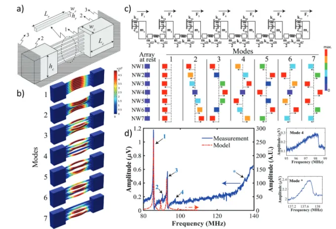
This work extends the use of mechanical coupling to the nanoscale by exploiting a new composite resonator architec-ture. For this purpose, a vertical stack of NWs clamped between a pair of coupling membranes is utilized. Components of the NEMS array architecture are shown in Fig. 1a. A series of double-anchored NWs are stacked perpen-dicular to the chip surface (Component 1). A pair of couplers in the form of coupling membranes are placed at both ends of the NW stack (Component 2). Each coupler is attached to a
rigid support (Component 3) along its side and bottom sur-faces. Finally, the NW stack is placed between a pair of side-gate electrodes to facilitate proper signal transduction. In-plane dimensions of all components are defined by lithogra-phy. Hence, they constitute the main set of parameters deter-mining the coupling strength through the mechanical compli-ance of the coupler and the overall resoncompli-ance characteristics of the NW array. These include the width and the length of the coupler, wcand Lc, respectively, and those of the NWs, wrand
Lr, respectively. The coupler thickness, hc, is equal to the
device layer thickness of the SOI (silicon-on-insulator) wafer, whereas the thickness of each NW, hr, is an outcome of the
scalloping effect of the deep etch process (see ESI Fig. S1†).29 The use of vertical NW stacks as composite resonators pre-sents a new approach towards 3D integration with promising implications for signal amplification, frequency engineering and sensing. The fact that the coupling strength can be tuned by lithography parameters is a significant advantage.30 Furthermore, this approach provides a platform to study fun-damental dynamics of strongly coupled systems including
Fig. 1 Concept of coupling. (a) A view of the coupled resonator array depicting (1) the vertical NW stack, (2) couplers in the form of coupling mem-branes, and (3) the rigid support. (b) Sevenflexural mode shapes of an array of seven NWs obtained by a finite-element model (FEM). Colour chart refers to relative deflection magnitudes. (c) Lumped-parameter model with each mass, mi, referring to distinct NW resonators andkiiandcii indicat-ing resonator stiffness and damping, respectively. Coupler mass and stiffness between the ithandjthNWs are indicated bym
cijandkij, respectively, with 1≤ i & j ≤ 7. Further discussion is provided in connection with ESI Fig. S2.† Resulting mode shapes depicted by the deflection of the vertical array of NWs from their positions at rest verify FEMfindings of Panel (b). Colour chart refers to displacements in arbitrary units. (d) Corresponding measurement of the frequency spectrum and lumped-parameter model prediction exhibiting several modes within a narrow frequency band. Insets demonstrate open-loop sweep results, taken with a different set of actuation voltages for clarity.
phenomena such as collective modes.20,31 Hence, the pro-posed coupling scheme addresses ongoing discussions and shortcomings caused by the lack of compact mechanical coup-ling with controllable stiffness at the nanoscale.27 Additionally, coupling membranes with minute in-plane dimensions result in a very compact structure. Switching from horizontal to vertical resonator stacks of Fig. 1a thus leads to a further reduction in device footprint and helps increase device density considerably. And unlike complicated filter designs,32 the use of coupling membranes facilitates the coupling of non-adjacent resonators in an array with enhanced spectrum characteristics of sharper roll-offs and improved stopband rejection. In this respect, the coupling scheme of this work makes a significant contribution to the rather limited mechan-ical coupling toolkit at the nanoscale by connecting all non-adjacent resonators effectively, and at once.
To clarify the coupling concept further, the finite-element model (FEM) of the particular stack of seven NWs of Fig. 1a is depicted in Fig. 1b, revealing seven flexural mode shapes. The corresponding nominal NW dimensions are 60 × 80 × 2000 nm (wr× hr× Lr) for a coupler length, Lc, of 1000 nm, and wcand
hc of 500 nm and 1 µm, respectively. Mode shape
modifi-cations due to coupler boundary conditions and NW dimen-sional variations within a stack are discussed in connection with ESI Fig. S3.† The same architecture can be analysed through the lumped-parameter model of Fig. 1c, yielding mode shapes that closely resemble those predicted by FEM. Colour charts are used to emphasize relative magnitudes of respective deflections of NWs within the array. Through the lumped-parameter model, one does not only obtain mode shapes but can also predict the spectral response. Details of both FEM and lumped-parameter model are provided in the ESI.†
Finally, frequency sweeps are conducted through dynamic piezoresistive measurements (see ESI Fig. S4†).33 A doping
level of 1020 cm−3 is employed at the SOI wafer surface. Electrostatic actuation is implemented using one of the two adjacent gate electrodes with a nominal gap of 180 nm. A fre-quency downmixing34 detection scheme, 2 source – 1ω,35 is used for piezoresistive readout at frequencies as high as 100 MHz. In this scheme, a function generator at the NEMS frequency is superimposed with a DC gate voltage to provide the driving signal. On the readout side, a second function gen-erator is used to bias the piezoresistor at a frequency slightly offset from the driving signal to generate a signal at the mix down frequency (typically at tens of kHz). Frequency spectrum measurements are performed in a vacuum chamber at a pressure level of lower than 10−7 Torr and at ambient temperature.
A typical frequency response curve is shown in Fig. 1d along with the corresponding lumped-parameter model pre-diction. The first four modes obtained within a narrow fre-quency band can indeed be detected. While one inset shows the frequency sweep for Mode 4 for clarity purposes, other peaks on the curve are found not to represent any resonance of mechanical nature up until Mode *, an out-of-plane flexural
mode as predicted by FEM. An inset is also provided to depict its details. Peaks were studied in terms of how well their response to changing parameters including vacuum level, drive signal’s amplitude and the type of readout (1ω vs. 2ω, see ESI Fig. S4†) would exhibit expected behaviour of mechani-cal resonance. Nonmechanimechani-cal peaks were thus excluded from the notation in Fig. 1d.
The study in Fig. S3† also reveals useful information regard-ing the lack of Modes 5, 6 and 7 in Fig. 1d. A strikregard-ing di ffer-ence exists between the ideal case (upper left panel) and the scenario with the closest resemblance to the experimental plat-form (lower right panel) in Fig. S3.† While almost a single NW resonates in these higher modes, no other resonator contrib-utes to signal transduction. Same physics is captured by the lumped-parameter model in Fig. 1d, as coupling stiffness and NW mass are gradually increased towards the substrate.
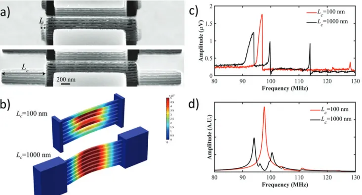
Having introduced the concept of coupling, modulation of the coupling strength is pursued next. For this purpose, the coupler length, Lc, is employed as the main design parameter.
As shown in Fig. 2a, a much stiffer coupler is now employed with Lc= 100 nm representing a ten-fold reduction compared
to the coupler length of the device of Fig. 1. The difference generated by this modification is evident from a comparison of mode shapes for Mode 1, as compliant coupling induces a much stronger interaction among NWs (Fig. 2b). This predic-tion is indeed verified by measurements. A comparison of resonance spectra for a series of samples with stiff (Samples 1 and 2) and compliant (Samples 3–5) coupling is provided in Table 1. While fewer number of modes are apparent in the stiff coupling case, compliant coupling generates a series of easily detected modes. One sample measurement can be found in Fig. 2c, where frequency sweeps conducted under the same set of conditions are depicted for both types of coupling. For stiff coupling, Mode 1 stands out, while higher-order modes become challenging to capture. High Q with lower Lc, as
dis-cussed later, is linked to high SNR of Mode 1. Thus, modes in Table 1 have to be interpreted by the lumped-parameter model as demonstrated in Fig. 1d. Similar to Mode * of Fig. 1d, higher modes beyond 130 MHz are expected to indicate out-of-plane flexural modes as predicted by FEM, hence, they cannot be numbered in accordance to Fig. 1b (see ESI for details†).
A further examination of Table 1 and the lumped-parameter model prediction of Fig. 2d reveals several modes dispersed in a narrow frequency range. In fact, such modes existing in close proximity can overlap through changing control voltages—a highly desirable feature for building sharp and tunable band-pass filters. An example of this observation is depicted in Fig. 3a, where the spectral response of a particular NW stack is tracked with respect to the gate AC voltage. Fig. 3a illustrates the emergence of two peaks from a single mode at a low voltage (Point A) and their eventual merging at a common non-linear mode (Point B) as the gate voltage increases progress-ively. Here, Point A represents the instance, when the low-SNR one of the two closely spaced peaks first shows up upon reach-ing the threshold drive signal. With further increase in actua-tion, both peaks exhibit shifting resonance frequencies until
the onset of nonlinearity at Point B. This evolution of the reso-nance frequency of each mode is then plotted with respect to the gate AC voltage in Fig. 3b. The initial linear variation of the high-SNR mode at low voltages is evident until mode splitting takes place at Point A, beyond which each mode follows its dis-tinct path. Hence, the dependence of the frequency spectrum on actuation differs significantly from the linear response of single NW resonators33,35 at high voltages. This trend was further verified by measurements (see ESI Fig. S5†) on NEMS stacks of very different coupling lengths or with different types of control voltages.
To obtain further insight into the nonlinear coupling between the mechanical subunits, intermodal coupling is
investigated next. Verified by FEM, the detected modes in Table 1 are assumed to have a flexural origin. Flexural motion of each fixed-fixed NW creates tension along its axis,36which, in turn, increases its effective stiffness. In the case of multiple flexural modes, they would be coupled to each other through this tension, and the frequency of one mode would be tuned
Fig. 2 Control of coupling strength. (a) Stacks of nominally identical NWs with stiff (Lc= 100 nm, upper micrograph) and compliant (Lc= 1000 nm, lower micrograph) coupling. (b) Shape of Mode 1 showing an increased level of interaction between NWs with increased coupler length,Lc, as pre-dicted by FEM. Colours refer to relative amplitudes of mechanical vibrations. (c) Spectral response comparison of stiff and compliant coupling, Samples 2 and 4 of Table 1, respectively, atVDC
gate= 15V, VACgate= 0.22VppandVACNW= 0.13Vpp. Some modes of Sample 4 in Table 1 are not clearly visible in the frequency spectrum due to lower actuation voltages utilized here. (d) The corresponding prediction of the lumped-parameter model high-lighting higher SNR for the lowest mode in the case of stiff coupling and higher number of modes detected in the case of compliant coupling.
Table 1 Detected modes of the NW stacks with their frequencies in MHz
Coupler type Sample Detected modes
Stiff (Lc= 100 nm) 1 99a 129 — — — — 2 95a 122 128 — — — Compliant (Lc= 1000 nm) 3 70a 77 108 122 128 — 4 87 91a 97 99 111 113 5 86a 90 93 98 138 143 aDenotes the mode with the highest SNR.
Fig. 3 (a) Evolution of the adjacent modes with respect to the peak-to-peak gate AC voltage,VAC
gate(Vpp), shows characteristics unlike the single NW case.36A mode splitting at A is induced until the onset of nonlinear-ity at B, where modes merge again at a common nonlinear mode. VDC
gate= 0.5V and VACNW= 0.3Vpp. (b) A closer view of split modes between Points A and B. For nonlinear peaks, the bifurcation point in the upward frequency sweep is reported.
depending on its coupling strength to the excited mode.37–41 Hence, a higher coupling strength is expected between two col-lective modes sharing common vibrating NWs.
To study this aspect of flexural modes further, the measure-ment setup of Fig. S4† is modified so that NW and gate voltage signals now have two components, one for each mode (see ESI Fig. S7†). Thus, as reported elsewhere,41one mode can now be kept at resonance using a phase-locked-loop (PLL) circuit, while an open-loop measurement is simultaneously performed for the second mode ( fsweep). This way, pumping mode i
induces a resonance frequency change (Δfj/fj) for the mode j,
such that the frequency change is proportional to the intermo-dal coupling strength (δij).
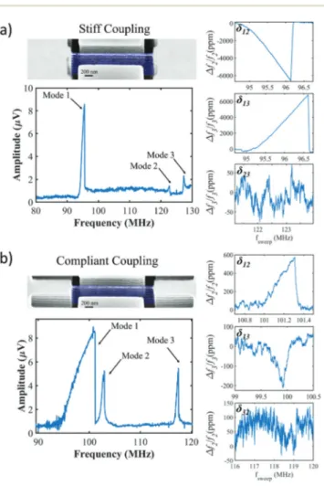
Fig. 4 compares resonance frequency shifts for a series of mode pairs in addition to an open-loop measurement for each coupling type. Results indicate a higher interaction between the highest SNR mode, Mode 1, and the remaining modes (δ12
andδ13) compared to those among the lower SNR modes (δ23),
for the same input drive levels. Some of the frequency shifts notably turn out to be negative (e.g.δ12in stiff coupling, and
δ13in compliant coupling cases). In sharp contrast with these
observations, isolated modes connected on the same anchor would yield only positive frequency shifts owing to the increased overall tension. Moreover, Modes 2 and 3 do not seem to couple to each other even in the case of compliant coupling, in spite of the fact that their SNR values are compar-able to that of the first mode (Fig. 4b). This observation is again difficult to reconcile with the weakly-coupled, isolated-modes picture, since the vibration of isolated NWs on the same anchor is expected to tune the tension in similar ways. In other words, as the vibration of isolated NWs would affect the overall tension within the array-coupler system in a similar fashion, the signs of the intermodal shifts would have been the same between any pair of modes. Interestingly, this expec-tation is violated by the results shown in Fig. 4. Due to the symmetrical placement of the drive gate, the actuation of higher harmonics of the same NW is not expected to occur. Even if this was the case, higher harmonics would have been detected at much higher frequencies than those reported here. On the other hand, the observed interaction strengths and signs can very well be accommodated within a framework of collective modes of NWs. Therefore, the sign of intermodal interactions supports the hypothesis that the observed modes are indeed the result of the collective vibrations of the array rather than the isolated vibrations of individual NWs. Hence, strong coupling between modes and tunable spectral response are evident in Fig. 4 and 3, respectively.
Conclusions
The excitation of a coupled vertical NW stack with a common side-gate electrode is used to detect several modes in a narrow frequency span. Due to the ability of tuning the coupling strength, compliant coupling is shown to enable the detection of a higher number of mechanical modes. When two such modes of a NW stack are in close proximity, a spectrum behav-iour similar to that of a bandpass filter is realized. Additional flexibility for shaping the passband is also demonstrated by modulating control voltages with diverging and coalescing peaks.
Intermodal coupling measurements indicate high coupling strengths between the highest SNR mode and remaining modes. Such high coupling strengths are useful in cases where tracking of several mechanical modes in a narrow frequency range is required to gather information such as inertial imaging of an analyte landed onto a nanomechanical resonator.42,43
Spectrum measurements for the case of stiff coupling reveal Qs on the order of 900 for the lowest mode under vacuum. However, additional energy sinking by the introduction of the compliant couplers reduces Qs to approximately 300 (see ESI Fig. S6†). This also explains high SNRs of Mode 1 with stiff coupling in Fig. 2. Thus, energy dissipation in couplers can be further suppressed to get higher Qs, for instance, by modifying the device design. As a specific example, the couplers of this
Fig. 4 Intermodal Coupling. Interactions between a series of mode pairs are studied for (a) stiff and (b) compliant coupling. Resonance fre-quency tuning of a phase-locked mode is tracked with respect to the frequency sweep of a pumped mode. Actuation details are given in the ESI.† NW stacks are colorized for clarity.
study are not released from the underlying buried oxide (BOX) layer, causing additional acoustic loss through the substrate. By releasing couplers using oxide dry etching, both the Q values and mechanical coupling between NWs are expected to increase. Nevertheless, signal responses from coupled NW modes are still obtained with existing devices. Moreover, the current annealing of devices in vacuum,44or the oxidation and subsequent dry etching of oxide on NWs45 can further enhance the electronic and dimensional uniformity of NWs.
As a future work, several coupled vertical stacks can be placed in a series configuration to realize electromechanical filters at the nanoscale. In this way, filter characteristics such as bandwidth can be adjusted reliably by means of a coupler connecting sequential stacks. Moreover, other boundary con-ditions such as free-free can be utilized to increase Q of the fre-quency response of the coupled NW stack.
Con
flicts of interest
There are no conflicts to declare.
Acknowledgements
Authors acknowledge financial support by TÜBİTAK under Grant no. 118E252. Technical support by Dr Karimzadehkhouei is grate-fully acknowledged.
References
1 T. Kouh, M. S. Hanay and K. L. Ekinci, Micromachines, 2017,8(4), 108.
2 D. F. Santavicca, J. K. Adams, L. E. Grant, A. N. McCaughan and K. K. Berggren, J. Appl. Phys., 2016,119(23), 234302. 3 G. Gourlat, M. Sansa, P. Villard, G. Sicard, G. Jourdan,
I. Ouerghi, G. Billiot and S. Hentz, in Proc. 2017 IEEE International Solid-State Circuits Conference (ISSCC), 5–9 Feb. 2017, pp. 266–267.
4 Y.-J. Seo, M. Toda and T. Ono, J. Micromech. Microeng., 2015,25(4), 045015.
5 M. S. Hanay, S. Kelber, A. K. Naik, D. Chi, S. Hentz, E. C. Bullard, E. Colinet, L. Duraffourg and M. L. Roukes, Nat. Nanotechnol., 2012,7(9), 602–608.
6 M. Yuksel, E. Orhan, C. Yanik, A. B. Ari, A. Demir and M. S. Hanay, Nano Lett., 2019,19(6), 3583–3589.
7 N. Delorme, C. L. Blanc, A. Dezzani, M. Bély, A. Ferret, S. Laminette, J. Roudier and E. Colinet, IEEE J. Solid-State Circuits, 2016,51(1), 249–258.
8 L. M. de Lépinay, B. Pigeau, B. Besga, P. Vincent, P. Poncharal and O. Arcizet, Nat. Nanotechnol., 2017,12(2), 156.
9 J. Chaste, A. Eichler, J. Moser, G. Ceballos, R. Rurali and A. Bachtold, Nat. Nanotechnol., 2012,7(5), 301–304.
10 J. Moser, J. Güttinger, A. Eichler, M. J. Esplandiu, D. E. Liu, M. I. Dykman and A. Bachtold, Nat. Nanotechnol., 2013, 8(7), 493–496.
11 M. Nasr Esfahani, Y. Leblebici and B. E. Alaca, J. Microelectromech. Syst., 2017,26(3), 624–631.
12 S. Dellea, P. Rey and G. Langfelder, J. Microelectromech. Syst., 2017,26(6), 1389–1399.
13 I. Mahboob, N. Perrissin, K. Nishiguchi, D. Hatanaka, Y. Okazaki, A. Fujiwara and H. Yamaguchi, Nano Lett., 2015,15(4), 2312–2317.
14 C. S. Lam, in Proc. 2016 IEEE International Frequency Control Symposium (IFCS), 9–12 May 2016, pp. 1–6. 15 J. M. L. Miller, D. D. Shin, H.-K. Kwon, S. W. Shaw and
T. W. Kenny, Phys. Rev. Appl., 2019,12(4), 044053.
16 A. Uranga, J. Verd and N. Barniol, Microelectron. Eng., 2015, 132, 58–73.
17 R. P. Middlemiss, A. Samarelli, D. J. Paul, J. Hough, S. Rowan and G. D. Hammond, Nature, 2016,531, 614. 18 M. Akgul and C. T. Nguyen, in Proc. 2014 IEEE
International Frequency Control Symposium (FCS), 19–22 May 2014, pp. 1–6.
19 W. Ark-Chew and C. T. Nguyen, J. Microelectromech. Syst., 2004,13(1), 100–112.
20 M. H. Matheny, J. Emenheiser, W. Fon, A. Chapman, A. Salova, M. Rohden, J. Li, M. Hudoba de Badyn, M. Pósfai, L. Duenas-Osorio, M. Mesbahi, J. P. Crutchfield, M. C. Cross, R. M. D’Souza and M. L. Roukes, Science, 2019,363(6431), 7932.
21 M. S. Hajhashemi, A. Rasouli and B. Bahreyni, J. Microelectromech. Syst., 2016,25(1), 52–59.
22 M. Spletzer, A. Raman, A. Q. Wu, X. Xu and R. Reifenberger, Appl. Phys. Lett., 2006,88(25), 254102. 23 C. Zhao, M. H. Montaseri, G. S. Wood, S. H. Pu,
A. A. Seshia and M. Kraft, Sens. Actuators, A, 2016,249, 93– 111.
24 J. Giner, A. Uranga, F. Torres, E. Marigo and N. Barniol, Electron. Lett., 2010,46(9), 640–641.
25 M. Mehrnaz, R. M. Raafat and K. Amir, J. Micromech. Microeng., 2006,16(2), 407.
26 D. Endo, H. Yabuno, K. Higashino, Y. Yamamoto and S. Matsumoto, Appl. Phys. Lett., 2015,106(22), 223105. 27 R. Yang and J. Lee, Z. Wang and P. X. L. Feng, in Proc.
2013 Joint European Frequency and Time Forum & International Frequency Control Symposium (EFTF/IFC), 21–25 July 2013, pp. 145–148.
28 J. Llobet, G. Rius, A. Chuquitarqui, X. Borrise, R. Koops, M. van Veghel and F. Perez-Murano, Nanotechnology, 2018, 29, 155303.
29 Z. Tasdemir, N. Wollschläger, W. Österle, Y. Leblebici and B. E. Alaca, Nanotechnology, 2016,27(9), 095303.
30 S. Stassi, G. De Laurentis, D. Chakraborty, K. Bejtka, A. Chiodoni, J. E. Sader and C. Ricciardi, Nat. Commun., 2019,10(1), 3647.
31 W. Fon, M. H. Matheny, J. Li, L. Krayzman, M. C. Cross, R. M. D’Souza, J. P. Crutchfield and M. L. Roukes, Nano Lett., 2017,17(10), 5977–5983.
32 L. Sheng-Shian, M. U. Demirci, L. Yu-Wei, R. Zeying and C. T. C. Nguyen, in Proc. 2004 IEEE International Frequency Control Symposium and Exposition, 23–27 Aug. 2004, pp. 280–286.
33 M. Nasr Esfahani, Y. Kilinc, M.Ç. Karakan, E. Orhan, M. S. Hanay, Y. Leblebici and B. E. Alaca, J. Micromech. Microeng., 2018,28(4), 045006.
34 I. Bargatin, I. Kozinsky and M. L. Roukes, Appl. Phys. Lett., 2007,90(9), 093116.
35 M. Sansa, M. Fernández-Regúlez, J. Llobet, Á. San Paulo and F. Pérez-Murano, Nat. Commun., 2014,5(1), 4313. 36 R. He, X. L. Feng, M. L. Roukes and P. Yang, Nano Lett.,
2008,8(6), 1756–1761.
37 M. Matheny, L. Villanueva, R. Karabalin, J. E. Sader and M. Roukes, Nano Lett., 2013,13(4), 1622–1626.
38 H. Westra, M. Poot, H. Van Der Zant and W. Venstra, Phys. Rev. Lett., 2010,105(11), 117205.
39 A. Eichler, M. del Álamo Ruiz, J. Plaza and A. Bachtold, Phys. Rev. Lett., 2012,109(2), 025503.
40 P. Truitt, J. Hertzberg, E. Altunkaya and K. Schwab, J. Appl. Phys., 2013,114(11), 114307.
41 A. B. Arı, M.Ç. Karakan, C. Yanık, I. I. Kaya and M. S. Hanay, Phys. Rev. Appl., 2018,9(3), 034024.
42 M. S. Hanay, S. I. Kelber, C. D. O’Connell, P. Mulvaney, J. E. Sader and M. L. Roukes, Inertial imaging with nano-mechanical systems, Nat. Nanotechnol., 2015, 10(4), 339– 344.
43 J. E. Sader, M. S. Hanay, A. P. Neumann and M. L. Roukes, Nano Lett., 2018,18(3), 1608–1614.
44 K. I. Bolotin, K. J. Sikes, J. Hone, H. Stormer and P. Kim, Phys. Rev. Lett., 2008,101(9), 096802.
45 D. Sacchetto, M. H. Ben-Jamaa, G. DeMicheli and Y. Leblebici, in Proc. 2009 European Solid State Device Research Conference, 14–18 September 2009, pp. 245–248.