First-principles study of thin TiO
xand bulklike rutile nanowires
D. Çakır and O. Gülseren*
Department of Physics, Bilkent University, Ankara 06800, Turkey
共Received 8 August 2008; revised manuscript received 29 August 2009; published 24 September 2009兲
We have systematically investigated structural, electronic and magnetic properties of very thin TiOx
共x=1,2兲 nanowires as well as bulklike 共110兲 rutile nanowires by using the first-principles plane-wave pseudo-potential calculations based on density functional theory. A large number of different possible structures have been searched via total-energy calculations in order to find the ground-state structures of these nanowires. Three-dimensional structures are more energetically stable than planar ones for both of the stoichiometries共i.e., x = 1 , 2兲. The stability of TiOxnanowires is enhanced with its increasing radius as a result of reaching sufficient coordination number of Ti and O atoms. All stoichiometric TiO2nanowires studied exhibit semiconducting behavior and have nonmagnetic ground state. There is a correlation between binding energy共Eb兲 and energy
band gap共Eg兲 of TiO2nanowires. In general, Ebincreases with increasing Eg. In TiO nanowires, both metallic
and semiconductor nanowires result. In this case, in addition to paramagnetic TiO nanowires, there are also ferromagnetic ones. We have also studied the structural and electronic properties of bulklike rutile 共110兲 nanowires. There is a crossover in terms of energetics, and bulklike nanowires are more stable than the thin nanowires for larger radius wires after a critical diameter. These共110兲 rutile nanowires are all semiconductors. DOI:10.1103/PhysRevB.80.125424 PACS number共s兲: 61.46.Km, 62.23.Hj, 73.22.⫺f, 75.75.⫹a
I. INTRODUCTION
Titania, TiO2, exits in a number of different crystalline forms, such as anatase, rutile and brookite. Thermodynami-cally, rutile is the most stable phase under ambient condi-tions. Since, it is nontoxic and environmentally clean, and because of its cheap production and stability under illumina-tion, titanium dioxide is widely used in many different tech-nological applications including self-cleaning coatings, pig-ments, sunscreens, toothpastes, photovoltaics, photocatalysis and photoelectrochemistry.1–3Surface properties and surface structure is very important for most of these applications. Therefore, increasing the surface area by producing the tita-nia nanoparticles and nanowires might be very crucial. In addition to this, novel properties due to the quantum size effect might arise from small diameter nanowires of titania. In recent years, one-dimensional 共1D兲 TiOx nanostructures3
such as nanorods, nanowires, and nanotubes have been in-vestigated extensively because of their size and morphology dependent structural, chemical and electronic properties. They lead to a significant number of technological applica-tions including gas and humidity sensors,4dye-sensitized so-lar cells,5,6photovoltaics, and photocatalysis.7
TiO2 nanowires8–13 can be synthesized on TiO
2 surfaces or in zeolites. Blanco-Rey et al.8 have obtained non-stoichiometric Ti2O3 quasi-one-dimensional metallic chains along the 关001兴 direction of 共1⫻2兲 reconstructed rutile surface. Naturally, semiconductor monatomic titania 共¯Ti-O-Ti-O¯兲 chains is formed in Engelhard titanosilicate-4 共ETS-4兲 共Ref. 9兲 and 10 共ETS-10兲.10 Indi-vidual chains are isolated from each other by an insulating silicate layer. Electrical transport measurement has been made for ETS-4 and a non-Ohmic behavior has been ob-served. Conductivity of these monatomic chains increases with increasing bias voltages. Recently, TiO2 atomic wires with a few angstroms diameter are synthesized by solution methods.13Structural, electronic and vibrational properties of
titania chains embedded in ETS-10 have been studied using ab initio methods.14Moreover, Enyashin et al.15,16have stud-ied the stability and electronic structure of various TiO2 nanotubes governed from anatase and lepidocricite layer modifications by using density-functional-based tight-binding method. Futhermore, ab initio calculations are re-ported that investigates atomic scale17 as well as the rutile18 TiO2 nanowires.
Therefore, a thorough analysis of the structural and elec-tronic properties of stoichiometric and nonstoichiometric ti-tania nanowires is necessary before one aims at its possible applications. Our motivation in this work is to understand how thin TiOx and rutile 共110兲 nanowires are formed and
their properties due to the dimensionality. This work presents a systematical investigation of structural, electronic and magnetic properties of these nanowires within the density-functional theory共DFT兲.
II. COMPUTATIONAL METHODS
Total-energy and electronic-structure calculations have been performed by first-principles plane-wave method19,20 based on DFT共Ref.21兲 using both ultrasoft22and projected-augmented-wave 共PAW兲 共Refs.23 and24兲 pseudopotentials
with electronic configurations 3p63d34s1 for Ti atoms and 2s22p4for O atoms. The exchange-correlation potential has been treated by generalized gradient approximation 共GGA兲.25All structures have been represented in a tetragonal supercell geometry共with lattice parameters asc= bsc and csc兲
using periodic boundary conditions. To prevent interaction between adjacent isolated wires, a large spacing 共asc= bsc
⬃16 Å兲 has been introduced. For single cell wire calcula-tions, csccorresponds to lattice constant c and for double cell
calculations csc= 2c共c being the lattice parameter of the TiOx
wires along the wire axis兲. Convergence with respect to the number of plane waves used in expanding Bloch functions and k points in sampling the Brillouin zone have been tested
for each wire systems. A plane-wave basis set with kinetic energy cutoffប2兩k+G兩2/2mⱕ450 eV has been used. In the self-consistent potential and total-energy calculations, Bril-louin zone of nanowires has been sampled by 共1⫻1⫻27兲 and 共1⫻1⫻17兲 meshes in the k space within Monkhorst-Pack scheme26for single and double unit cells, respectively. In order to treat partial occupancies, Methfessel-Paxton smearing method27 is used. The width of smearing has cho-sen as 0.08 eV for geometry relaxation and 0.01 eV for ac-curate energy band and electronic density of states calcula-tions. All atomic positions and lattice parameters have been optimized by using conjugate gradient method where total energy and atomic forces are minimized. The convergence for energy has been chosen as 10−5 eV between two ionic steps, and the maximum force allowed on each atoms is 0.03 eV/Å.
III. RESULTS AND DISCUSSIONS
First of all, pseudopotential of Ti and O atoms have been tested. Calculated lattice parameters and energy band gap 共Eg兲 of bulk rutile and anatase phases with two different
exchange-correlation functionals关GGA and local-density ap-proximation共LDA兲兴 have been compared with available ex-perimental data28–30 in Table I. Due to pseudopotentials, exchange-correlation approximation and methods used in calculations, lattice parameters can be slightly different from both experimental28–30 and previous calculated values.31–34 The comparison of these results, similar to some recent studies35,36 comparatively including several different exchange-correlation functionals as well as pseudopotentials suggests that GGA calculations yield slightly better agree-ment with experiagree-mental data. Hence, using GGA approxima-tion, the calculated lattice parameters a and c of rutile are 4.64共4.59兲 and 2.98共2.96兲 Å, respectively. The experimental values28–30are quoted in parentheses. For the case of anatase, a and c values are 3.81共3.79兲 and 9.76共9.51兲 Å which are in fair agreement with experimental values.29,30 Compared to the experimental data, maximum deviation appears with ana-tase c parameter 共2.6%兲 while the variation in all the other lattice parameters from experimental values are less than 1%. Egvalues are 1.90共3.03兲 eV for rutile and 2.30 共3.2兲 eV for
values.39 Bent TiO
2 molecule is about 2 eV energetically more stable than linear one and both structures prefer the singlet state. Ti–O bond length and O–Ti–O bond angle are 1.66 Å and 109°共1.64 Å and 109° with LDA兲, respectively. Experimentally estimated value40 of O–Ti–O angle is 110⫾5. Ti–O–O–Ti structure is unstable in linear Ti2O2 molecule. Upon relaxation of linear Ti–O–O–Ti molecule, two separated Ti–O molecules resulted by breaking O–O bond. In Ti–O molecule, Ti atom donates two electrons to O atom. According to Hund’s rule, remaining unpaired d elec-trons of Ti cause to magnetization in this molecule. In con-trast to TiO molecule, Ti atom gives all the valance electrons to p orbitals of two O atoms in TiO2molecule. As a result of this charge transfer, TiO2 is a closed shell molecule and has paramagnetic ground state.
A. (TiO)nnanowires
Several single and double stranded 共TiO兲n wires are
in-vestigated, and their optimized structures are presented in Fig. 1. Wire structures include both simple and more com-plicated structures together. In order to quantify the relative stabilities of these wires, binding energy Ebper formula unit
共f.u.兲 for 共TiO兲nwires is calculated in terms of the total
en-ergy of wire, ET关共TiO兲n兴, and the energies of individual
at-oms, E关Ti兴 and E关O兴 for Ti and O atoms respectively, as, Eb= ET关共TiO兲n兴/n − E关Ti兴 − E关O兴 共1兲
where n represents the number of TiO block in the unit cell. Variation in Eb with lattice constant c along the wire axis is
shown in Fig. 2. It is noticed that there are two different regions along the energy axis in Fig. 2. First region is be-tween −10 and −10.5 eV and related to the single stranded wires. Double stranded nanowires are observed in the second region which is approximately 1 eV lower in energy than the previous one. Along the series of single stranded wires, Ti atom is undercoordinated compared to the bulk structures, and coordination number is varied between one and three, depending on the structure. Remember that in bulk TiO2, Ti and O atoms are sixfold and threefold coordinated, respec-tively. On the other hand, in double stranded systems which are more energetically stable, coordination number of Ti at-oms becomes four. Therefore, we can infer that coordination number influences the strength of binding in these wires. In each region, three-dimensional共3D兲 wires 共B6, B7, C3, C4兲 are more stable than planar 共B1, B2, B3, B4, B5, C1, and C2兲 wire structures. Existence of monovalent O or Ti atoms
GGA 3.81 9.76 2.30 4.64 2.98 1.90
LDA 3.75 9.50 2.22 4.57 2.94 1.93
also affect the binding. B5 and B6 structures have both monovalent Ti and O atoms. Coordination number of these monovalent atoms is one. Formal oxidation states of Ti and
O atoms are 共+4兲 and 共−2兲, whereas in the structures with TiO units, formal oxidation states of Ti and O atoms are 共+2兲 and 共−2兲. As a result, these monovalent atoms are un-dercoordinated and these atomic sites might be very reactive against to adsorbate atomic and molecular species. For the double stranded wires, our initial starting geometry for struc-tural minimization was planar, however for C3 and C4 wires planar structure is not preserved during the geometry optimi-zation.
Lattice parameter along the nanowire axis, some bond angles and interatomic bond distances between the atoms labeled in Fig.1, magnetic properties and Ebof共TiO兲nwires
at their ground states are summarized in TableII. Bulk tita-nium monoxide is also included in this Table for comparison. Bulk TiO crystal structure is ␣-TiO, that is a monoclinic phase which can be derived as ordered vacancies 共⬃15%兲 from simple sodium chloride with formula Ti5O5.41–43 Due
FIG. 2. 共Color online兲 Variation in binding energy, Eb共eV/f.u.兲,
with the lattice constant c in different共TiO兲nwires. Lattice constant
of B4c structures is multiplied by 0.5 in order to present all the data with a compact horizontal axis.
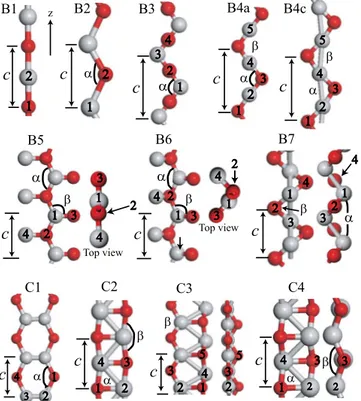
FIG. 1.共Color online兲 Optimized geometric structure of isolated 共TiO兲nnanowires. Assigned labels are indicated in order to identify
each of the wire. Light 共gray兲 and dark 共red兲 balls are used to represent Ti and O atoms, respectively. Lattice constant c, distance between the numbered atoms and indicated angles␣ and  at equi-librium are compiled in TableII.
TABLE II. Optimized lattice constant c0共in Å兲, interatomic bond distances d1–2, d1–3, d2–3, d1–4, d2–4, and d4–5共in Å兲, angles␣ and  共in degree兲, and binding energies Eb共in eV/f.u.兲 of 共TiO兲nnanowires. Magnetic
moment共兲 of the ferromagnetic wires are presented in terms of Bohr magneton B.
Wire c0 d1–2 d1–3 d2–3 d1–4 d2–4 d4–5 ␣  Eb B1 3.7 1.85 −10.13 2 B2 3.4 1.83 136.6 −10.26 2 B3 6.6 1.84 1.84 3.30 128.0 −10.21 4 B4a 5.75 1.85 1.85 2.88 2.88 101.5 101.8 −10.21 2.47 B4b 5.75 1.85 1.86 2.9 2.85 102.6 100.7 −10.22 2.47 B4c 5.7 1.83 1.88 2.86 2.86 100.8 100.8 −10.22 2.47 B5 3.5 1.95 1.64 1.87 127.7 116.3 −10.12 2.87 B6 3.5 1.95 1.65 1.91 128 114.1 −10.27 2 B7 4.15 1.84 2.62 1.85 104.9 90.4 −10.37 C1 3.2 1.82 2.70 4.44 122.8 −11.12 C2 3.9 1.98 2.93 1.94 2.62 83.0 166.1 −11.14 C3 3.1 2.00 3.31 1.84 1.93 2.78 2.81 67.4 115.2 −11.15 1.05 C4a 3.55 2.00 2.98 1.93 2.59 82.0 133.9 −11.16 2.19 C4b 3.55 2.02 2.99 1.91 2.54 80.6 136.1 −11.24 ␣-TiO 2.00–2.13 −13.01 Cubic TiO 2.14 −12.91
energy upon formation of internal Ti zigzag chain. B7 struc-ture can be obtained by compression of B4 chain. It can be easily seen from Fig.1or TableIIthat lattice constant of B3 chain is the largest. One of the O共Ti兲 atom in doubled unit cell of B2 is rotated 180° to obtain B3 共B4兲 structure. In other words, the B3 or B4 wires are formed by combining linear O–Ti–O units which have larger total energy than bent O–Ti–O units 共see B2 structure兲. On the other hand, in B4 structure, repulsive O–O interaction is small relative to B3 wire. Hence, the lattice constant of B4共B3兲 structure is very large compared to other single stranded wires in order to minimize repulsive O–O interaction that would compensate the energy loss due to the linear O–Ti–O units.
Most of the structures have magnetic ground state. How-ever, in both single and double stranded wires, nonmagnetic wires共B7 and C4b兲 have the lowest energy. In C4 structure, energy difference between the magnetic共C4a兲 and nonmag-netic states 共C4b兲 is 193.6 meV. Structural parameters of these magnetic and nonmagnetic isomers are not so different. B4 isomers have almost equal magnetic moment which is
= 2.47B, while the related wire structure B3 has the
larg-est magnetic moment, 4B. Magnetic moment of B1 and B2
are 2B. On the contrary, ground state of bulk TiO structure
is paramagnetic.
In general,共TiO兲nwires exhibit metallic behavior as seen
in Fig.3 while C1, C4b, B3 and B7 structures are semicon-ductor. Figures3共a兲–3共d兲 show the electronic band structure of double stranded wires whereas the ones of single stranded wires are collected in Figs.3共e兲–3共h兲. In the band structure of lowest energy structure, C4b, conduction band and valance band edges are very close to the EF at⌫ and Z points,
re-spectively. Eg is 0.19 eV and has indirect nature for this
nanowire. In most of the band structures, there are couple of bands below the Fermi level, EF, and then a large band gap
of a few eV’s occurs. For example, in the electronic band structure of C4b wire shown in Fig.3共d兲, there are two bands located just below the EFbefore a band gap of approximately
4 eV, and they are occupied by 4 electrons. If we remove four electrons one by one from C4b wire, EFgoes down in
energy in the calculated band structure of charged C4b nano-wire, and eventually wire becomes a semiconductor. A simi-lar situation happens for the other共TiO兲n nanowires.
There-fore, it is possible to infer that the stability of 共TiO兲n wires
might be enhanced upon adsorption that yield a charge trans-fer from these wires. Interestingly, B6 exhibits half metallic behavior. While, this nanowire is metallic for the spin up electrons, it is an indirect band-gap semiconductor with a Eg
of 0.74 eV for spin down electrons.
B. (TiO2)nnanowires
A large number of different possible initial wire geom-etries have been optimized by conjugate gradient minimiza-tions in order to find the ground-state structures of 共TiO2兲n
nanowires. Total energy of these structures is minimized with respect to lattice constant along the wire axis as well. Opti-mized nanowire geometries are presented in Fig. 4. Similar to the TiO wires, Eb per f.u. of 共TiO2兲n wires have been
calculated in terms of the total energy of wire, ET关共TiO2兲n兴,
and the energies of individual atoms, E关Ti兴 and E关O兴 for Ti and O atoms, respectively, as,
Eb= ET关共TiO2兲n兴/n − E关Ti兴 − 2E关O兴 共2兲
where n is the number of TiO2 block in the unit cell. Eb
versus lattice constant c along wire axis is illustrated in Fig.5.
Lattice parameter along the nanowire axis, bond angle and interatomic bond distances between the atoms labeled in Fig.4, binding energy Eb, and energy band gap Egof共TiO2兲n
wires at their ground states are summarized in TableIII. The stability and possibility of formation of TiO2nanowires can be investigated by comparing Ebof these nanowires with that
of bulk phases of TiO2. It is known that rutile phase of titania is thermodynamically more stable than anatase phase. Ebper
f.u. for rutile phase is −20.51 eV. The binding energy with respect to the cohesive energy of bulk rutile phase, Eb
r , might be defined as Eb wire − Eb rutile . Here, Eb wire and Eb rutile are the binding energies of an isolated nanowire and rutile bulk tita-nia. Eb
r
is also included in TableIII. Eb
r⬎0 means that bulk
rutile is more stable than a particular wire structure. It is observed that Eb
r
is positive for all TiO2 nanowires. But in our calculations, the total energy, not the free energy of these phases has been calculated.
The A1 and A2 wires have related structures. In a double cell of A1 geometry, one of the low-coordinated O atoms is rotated by 180° with respect to the other low-coordinated O atom to obtain the A2 structure. Difference between Eb’s of FIG. 3. 共Color online兲 The band structure of the selected 共TiO兲n wires. Fermi level of metallic systems shown by dashed lines mark the zero of energy. For magnetic systems, majority共minority兲 spin components are represented with dark solid共orange dashed兲 lines.
these two structures increases 共decreases兲 when lattice con-stant decreases共increases兲. For larger lattice constants, inter-action between the two low-coordinated O atoms decreases in the A1 structure. As a result, Eb’s of A1 and A2 begin to
get closer to each other. The difference between Eb’s of A1
and A2 geometries at equilibrium is 168.6 meV. The distance between adjacent O atoms affects the stability of wires. O atom prefers to make its coordination at least two. A1 and A2 wires have monovalent O atoms. Relative stability of these isomers is reduced by these monovalent atoms. Ti–O bond length共d1–2兲 between monovalent O and the nearest Ti atom is 10% shorter than other nearest-neighbor bond distances as seen in TableIII.
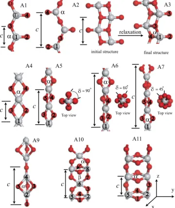
A double strand wire is formed by combining two A1 wires, this initial structure of A3 wire is not stable. The struc-tural optimization starting from this planar geometry yield either A3 wire shown in Fig.4or two separate weakly inter-acting A1 nanowires. When the planar geometry is con-strained during the optimization, the structure is transformed into two separated A1 structures. However, the former is energetically more favorable than the latter. The structures of A4 and A5 wires resemble to each other. In the A5 structure, one of the in-plane O pairs, namely O共2兲 and O共3兲, has been rotated by 90° with respect to the other in-plane O pair, O共4兲
FIG. 5. 共Color online兲 Variation in Eb共eV/f.u.兲 with respect to
the lattice constant c along the wire axis in different共TiO2兲n nano-wire structures. Lattice constant of A1, A3, A4, and A11 structures are multiplied by 2 in order to present all the data with a compact horizontal axis.
FIG. 4. 共Color online兲 Atomic structure of isolated 共TiO2兲n
wires. Assigned labels are indicated in order to identify each of the wire. Light共gray兲 and dark 共red兲 balls are used to represent the Ti and O atoms, respectively. Lattice constant c, distance between the numbered atoms and indicated angle␣ at equilibrium are summa-rized in TableIII.
TABLE III. Optimized lattice constant c0共in Å兲, interatomic bond distances d1–2, d2–3, d1–3, d1–4, d2–4, d2–5, and d3–5共in Å兲,␣ 共in degree兲, binding energies Eband Ebr 共binding energy with respect to rutile bulk
binding energy兲 共in eV/f.u.兲 of 共TiO2兲nnanowires. The energy band gap共in eV兲 of the semiconducting wires are also reported. Ebof rutile bulk phase is included for comparison. The definitions of Eband Ebr are given
in the text. Wire c0 d1–2 d2–3 d1–3 d1–4 d2–4 d2–5 d3–5 ␣ Eb Eb r Eg A1 3.45 1.64 1.88 3.45 133.6 −17.37 3.14 1.98 A2 6.70 1.65 1.86 6.70 128.1 −17.47 3.04 1.96 A3 3.65 1.64 1.98 1.99 84.5 −18.60 1.91 2.45 A4 2.85 1.89 2.48 2.85 82.1 −17.33 3.17 0.8 A5 5.45 1.85 2.51 3.25 85.4 −19.30 1.20 2.98 A6 8.25 1.86 2.51 3.00 84.7 −18.89 1.62 A7 11.1 1.87 2.5 2.9 84.2 −18.43 2.06 A9 6.10 1.85 1.89 2.40 2.49 79.7 −18.44 2.07 2.52 A10 6.35 1.82 1.83 2.55 2.60 88.8 −18.09 2.42 1.33 A11 3.28 1.85 2.48 1.84 2.72 84.6 −19.76 0.74 3.68 Rutile −20.51 0.00 1.90
Eb per f.u. increases with increasing number of TiO2 units. Therefore, infinite A5 wire is the upper limit of Eb in these
cluster model of A5 wires.
We have also formed the helical structures 共A6, A7, and A8兲 from A4 wire in order to investigate the relative stability of A4 and A5 structures. Each O pair has been rotated with respect to nearest O pairs with a rotation angle ␦ of 60° in A6, 45° in A7 and 36° in A8 structure as seen in Fig.4. The distance d2–4 in A6, A7, and A8 wires is longer than that in the A4 structure. The distance d2–3 affects the coupling be-tween the in-plane O atoms. When it is compared within the series of A4 to A8 wires, the value of d2–3starts to decrease from A5 and reaches its minimum value at A4 wire. So, it is the longest共shortest兲 in the A4 共A5兲 structure. Bond lengths d1–2and d2–3in A6, A7, and A8 wires are between d1–2and d2–3of the A4 and A5 wires. Therefore, helical structures are energetically more stable than A4. Eb reaches its maximum
value when␦= 90°. Ebof these helical structures are between
those of A4 and A5. While A4 wire sets the lower limit of Eb,
upper limit of Eb occurs at A5 structure. A8 structure does
not preserve the initial helical structure and tends to change its structure to A5. Hence, as a result of structural optimiza-tion, we have obtained an irregular helical structure for this case.
Coordination number of Ti atoms also strongly influences the binding of nanowires. Binding increases with increasing coordination of Ti atoms. For example, in A2 and A4 geom-etries, the coordination number of Ti is three and four, re-spectively. Coordination number also changes the bond lengths, the bond lengths increase when the coordination number of atoms increases. When the monovalent O atoms in the A1 and A2 structures are removed, one obtains the TiO zigzag chain presented in Fig. 1. Due to the monovalent O atom, d1–3in A1 is 2.7% longer than d1–2in TiO zigzag wire. The bond angle␣in A1 is 2.2% smaller than the bond angle in TiO zigzag structure. Consider the B3 wire formed upon removal of the monovalent O atoms of the A2 structure. The lattice constants of B3 and A2 structures differ only by 0.1 Å. Energy gain Egain of B3 wire at equilibrium upon
adsorption of two O atoms can be calculated with the follow-ing formula: Egain=共ET关A2兴+2E关O兴−ET关B3兴兲. ET关A2兴 and
ET关B3兴 are the total energies of A2 and B3 wires at c
= 6.6 Å. The energy gain upon adsorption of two O atoms to Ti atoms共atom 1 and atom 3 shown in Fig.1兲 in B3 wire is
14.51 eV.共TiO2兲n and共TiO兲nwires can be transformed into
each other by adding or removing O atom. However, Ti and O atoms tend to reach the sufficient coordination number to support their formal oxidation states. Therefore,共TiO兲nwires
gain huge energy upon adsorption of O atoms.
In general, TiO2 nanowires tend to form 3D structures. Planar structures have relatively lower binding energy than 3D structures. Compared to the other wires, the energy of the wire does not change so much upon compression or stretch-ing of A1, A2, A3, and A11 wires as seen in Fig. 5, and similarly B5, B6, and B7 TiO nanowires as depicted in Fig.
2. Variation in Ebwith respect to the lattice constant c along
the wire axis is wider and shallower for these wires. In the A5 case, the distance between O共2兲 and O共3兲 关or O共4兲–O共5兲兴 atoms decreases, while wire is being pulled along the z axis. As a result of the increase in the repulsive O–O interaction during stretching, Eb rises rapidly compared to A3 or A11.
Magnetic properties have also been investigated for all wire geometries. All studied wires have nonmagnetic ground state in their equilibrium structures.
Electronic properties of 共TiO2兲n wires are explored by
band structure calculations, and the relation between elec-tronic properties and stability of these wires is investigated. Electronic band structures of some selected nanowires are presented in Fig. 6. As inferred from Fig. 6, all studied 共TiO2兲n nanowires are semiconductors. Energy band gaps,
Eg, range from 0.8 to 3.68 eV compared to the 1.90 eV
calculated band gap of bulk rutile. There is a direct correla-tion between Eg and Eb. In general, Eg increases with
in-creasing Eb. We have examined in detail how the band
struc-tures are modified between similar strucstruc-tures关共A1, A2, A3兲 and共A4, A5兲兴. For example, there is a dramatic differences between the band structures of A4 and A5 wires. In the A4 structure, the band gap has indirect nature and the value of Eg is about 0.8 eV. Egis about 2.98 eV for A5 wire,
more-over its character is changed to a direct band gap. Remember that Ebof A5 is 1.97 eV lower than the one of A4 wire. The
band-gap behavior with different rotation angles,␦, of one of the O pair共see Fig.4兲 of A4 or A5 wire is studied in detail
and is presented in Fig. 7. The equilibrium structure of A5
FIG. 6.共Color online兲 The band structure of the selected 共TiO2兲n nanowires. Fermi level of these semiconductor wires are shown by dashed lines mark the zero of energy which indicates the top of the valence band.
共A4兲 is taken, and one of the O pair is rotated gradually ending up in the A4共A5兲 structure. Electronic band structure calculations are carried out without relaxing the modified structures. Doubled unit cell is used for the calculations of the A4 structure for direct comparison with the A5 results. This way, as displayed in Fig. 7, two different Eg versus
rotation angle ␦ curves are resulted depending on the path, i.e., starting from A5 structure and ending with A4 wire or vice versa. Eg’s of these rotated structures are between those
of A4 and A5 wires. Eg decreases from A5 to A4. Hence,
electronic structure is very sensitive to rotation, elongation, and contraction in the A4 and A5 structures. So, it is possible to tune the electronic properties of these wires by applying tension.
A1 and A2 structures have similar electronic band struc-tures. Nature of the band gap is direct. Eg of A1 and A2 is
1.98 and 1.96 eV, respectively. A3 is more stable than A1 and A2. Hence, it is expected that it has a relatively large Eg,
which is calculated as 2.45 eV. A11 structure is the most stable structure. Its Eg is 3.68 eV and the band gap is
indi-rect. In 共TiO2兲nwires, Ti and O atoms have 10共p6d3s1兲 and
6共s2p4兲 valence electrons, respectively. Ti atoms donate their four electrons to two O atoms to fill the unoccupied states of O atom. This behavior causes the semiconductor nature of 共TiO2兲n wires.
Stoichiometric and nonstoichiometric thin Ti–O wires can be formed on TiO2 surfaces upon reconstruction or anneal-ing. Therefore, it is important to understand structural, mag-netic, and electronic properties of these nanowires. Unlike stoichiometric TiO2nanowires, Ti2O3quasi-one-dimensional chains formed on reconstructed rutile 关110兴 surface exhibit metallic behavior.8 Moreover, we have both metallic and semiconducting共TiO兲nnanowires. As a result, it is expected
that stoichiometry strongly influences the electronic proper-ties of Ti–O nanowires.
C. Bulklike rutile (110) nanowires
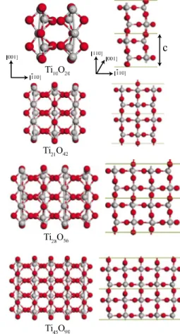
Finally, we have studied the structural and electronic properties of bulklike TiO2 nanowires. We considered bulk-like rutile 共110兲 nanowires, since, recently these wires are experimentally realized and synthesized.11 The nanowires
studied here have been cut in rodlike forms from the ideal bulk rutile crystal. Nanowires are oriented along the rutile 关110兴 crystallographic direction and each nanowire has dif-ferent diameter. All of them have rectangular cross-section and they have two 共110兲 and 共001兲 lateral surfaces. It is known that 共110兲 surface is the most stable surface among the rutile surfaces. Figure8shows the optimized structure of some of these nanowires. We have calculated the Ebof these
1D structure as a function of number of TiO2 units. It is important to figure out how the stability and electronic prop-erties of these nanowires evolve as the cross-section changes. The comparison of Ebof A5, A11, and TiO2bulklike nano-wires is shown in Fig. 9. It is noticed that bulk wires are energetically more stable than A5 structure. However, A11
FIG. 7. 共Color online兲 Variation in band gap Eg of A4 and A5
wires with the rotation angle ␦ which is the angle among O1– T2–O3 atoms共see Fig.4兲.
FIG. 8. 共Color online兲 Top and side view of the optimized geo-metric structure of the bulklike TiO2nanowires extended along the rutile关110兴 direction. Grey and red balls are used to represent the Ti and O atoms, respectively.
FIG. 9. 共Color online兲 Comparison of the atomically thin and bulklike TiO2nanowires. Eband Egare given in eV.
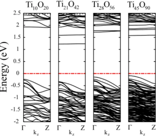
structure is slightly more stable than Ti10O20 and Ti21O42 nanowires. There is a crossover after the Ti21O42 nanowire, and the bulk wires with larger radius than this nanowire be-come more energetically stable. Internal regions of Ti28O56 and Ti45O90nanowires exhibit more bulklike behavior. Rutile phase is 0.5 eV more energetic than Ti45O90nanowire. Struc-tural distortion of initial structure of bulklike wires upon geometry optimization decreases as the cross-section in-creases. In Fig. 10, we have shown the band structure of these rutile 共110兲 nanowires. Bands around the Fermi level EFhas mainly O 2p character. The lowest conduction bands
are very flat and has d character. Except Ti10O20, all nano-wires have direct gap. In Ti10O20case, indirect energy gap is slightly smaller than direct one. Eg of these nanowires is
about the relative stability of the atomically thin stoichio-metric TiO2 nanowires, we have also studied the bulklike rutile 共110兲 nanowires, which are cut in a rodlike structure from crystalline rutile bulk and oriented along the关110兴 crys-tallographic direction. These bulklike nanowires become en-ergetically more stable with respect to thin nanowires after a certain cross-section, and all of them are semiconductors. Eg
of these thick nanowires oscillates around the computed Eg
of bulk rutile. Nonstoichiometric thin TiO wires have been also studied. They exhibit various electronic and magnetic properties. There are both metallic and semiconducting wires. Unlike stoichiometric titania nanowires, some of the TiO wires have magnetic ground state.
ACKNOWLEDGMENTS
Part of the calculations has been carried out at ULAKBIM Computer Center and UYBHM at Istanbul Technical Univer-sity. O.G. acknowledges the support of Turkish Academy of Sciences, TÜBA.
1U. Diebold, Surf. Sci. Rep. 48, 53共2003兲.
2T. L. Thompson and J. T. Yates, Jr., Chem. Rev. 共Washington, D.C.兲 106, 4428 共2006兲.
3X. Chen and S. S. Mao, Chem. Rev. 共Washington, D.C.兲 107, 2891共2007兲.
4G. Wang, Q. Wang, W. Lu, and J. Li, J. Phys. Chem. B 110, 22029共2006兲.
5B. Tan and Y. Wu, J. Phys. Chem. B 110, 15932共2006兲. 6J. Jiu, S. Isoda, F. Wang, and M. Adachi, J. Phys. Chem. B 110,
2087共2006兲.
7S. P. Albu, A. Ghicov, J. M. Macak, R. Hahn, and P. Schmuki, Nano Lett. 7, 1286共2007兲.
8M. Blanco-Rey, J. Abad, C. Rogero, J. Mendez, M. F. Lopez, J. A. Martin-Gago, and P. L. de Andres, Phys. Rev. Lett. 96, 055502共2006兲.
9B. Yilmaz, J. Warzywoda, and A. Sacco, Jr., Nanotechnology
17, 4092共2006兲.
10B. Yilmaz, A. Sacco, Jr., and J. Deng, Appl. Phys. Lett. 90, 152101共2007兲.
11S. S. Amin, A. W. Nicholls, and T. T. Xu, Nanotechnology 18, 445609共2007兲.
12B. Poudel, W. Z. Wang, C. Dames, J. Y. Huang, S. Kunwar, D. Z. Wang, D. Banerjee, G. Chen, and Z. F. Ren, Nanotechnology
16, 1935共2005兲.
13C. Liu and S. Yang, ACS Nano 3, 1025共2009兲.
14A. Damin, F. X. L. Xamena, C. Lamberti, B. Civalleri, C. M. Z. Wilson, and A. Zecchina, J. Phys. Chem. B 108, 1328共2004兲. 15A. N. Enyashin, V. V. Ivanovskaya, Y. N. Makurin, V. G.
Bam-burov, and A. L. Ivanovskii, Dokl. Phys. Chem. 391, 187 共2003兲.
16A. N. Enyashin and G. Seifert, Phys. Status Solidi B 242, 1361 共2005兲.
17D. Zhang, P. Liu, and C. Liu, J. Phys. Chem. C 112, 16729 共2008兲.
18H. Peng and J. Li, J. Phys. Chem. C 112, 20241共2008兲. 19M. C. Payne, M. P. Teter, D. C. Allen, T. A. Arias, and J. D.
Joannopoulos, Rev. Mod. Phys. 64, 1045共1992兲. 20Numerical computations have been carried out by using
VASP
software: G. Kresse and J. Hafner, Phys. Rev. B 47, 558共1993兲; G. Kresse and J. Furthmüller, ibid. 54, 11169共1996兲.
21W. Kohn and L. J. Sham, Phys. Rev. 140, A1133 共1965兲; P. Hohenberg and W. Kohn, ibid. 136, B864共1964兲.
22D. Vanderbilt, Phys. Rev. B 41, 7892共1990兲. 23P. E. Blöchl, Phys. Rev. B 50, 17953共1994兲.
24G. Kresse and D. Joubert, Phys. Rev. B 59, 1758共1999兲. 25J. P. Perdew and Y. Wang, Phys. Rev. B 45, 13244共1992兲. 26H. J. Monkhorst and J. D. Pack, Phys. Rev. B 13, 5188共1976兲. FIG. 10. 共Color online兲 The band structure of the various
bulk-like rutile 共110兲 nanowires. Fermi level is represented by dotted-dashed lines.
27M. Methfessel and A. T. Paxton, Phys. Rev. B 40, 3616共1989兲. 28S. C. Abrahams and J. L. Bernstein, J. Chem. Phys. 55, 3206
共1971兲.
29J. K. Burdett, T. Hughbanks, G. J. Miller, J. W. Richardson, Jr., and J. V. Smith, J. Am. Chem. Soc. 109, 3639共1987兲. 30C. J. Howard, Z. M. Sabine, and F. Dickson, Acta Crystallogr.,
Sect. B: Struct. Sci. 47, 462共1991兲.
31S. J. Thompson and S. P. Lewis, Phys. Rev. B 73, 073403 共2006兲.
32A. Kiejna, T. Pabisiak, and S. W. Gao, J. Phys.: Condens. Matter
18, 4207共2006兲.
33S. P. Bates, G. Kresse, and M. J. Gillan, Surf. Sci. 385, 386 共1997兲.
34T. Bredow, L. Giordano, F. Cinquini, and G. Pacchioni, Phys. Rev. B 70, 035419共2004兲.
35F. Labat, P. Baranek, and C. Adamo, J. Chem. Theory Comput.
4, 341共2008兲.
36H. Perron, C. Domain, J. Roques, R. Drot, E. Simoni, and H.
Catalette, Theor. Chem. Acc. 117, 565共2007兲.
37H. Tang, F. Levy, H. Berger, and P. E. Schmid, Phys. Rev. B 52, 7771共1995兲.
38A. V. Emeline, G. V. Kataeva, V. K. Ryabchuk, and N. Serpone, J. Phys. Chem. B 103, 9190共1999兲.
39K. P. Huber and G. Herzberg, Molecular Spectra and Molecular Structure共Van Nostrand Reinhold, New York, 1979兲, Vol. IV. 40N. S. McIntyre, K. R. Thompson, and W. Weltner, Jr., J. Phys.
Chem. 75, 3243共1971兲.
41D. Watanabe, J. R. Castles, A. Jostsons, and A. S. Malin, Acta Crystallogr. 23, 307共1967兲.
42C. Leung, M. Weinert, P. B. Allen, and R. M. Wentzcovitch, Phys. Rev. B 54, 7857共1996兲.
43J. Graciani, A. Márquez, and Javier Fdez. Sanz, Phys. Rev. B
72, 054117共2005兲.
44K. S. Jeong, C. Chang, E. Sedlmayr, and D. Sülze, J. Phys. B 33, 3417共2000兲.