MICROFABRICATION OF MICRO HALL
SENSORS ON GAAS AND INSB FOR
SCANNING HALL PROBE MICROSCOPY
a thesis
submitted to the department of physics
and the institute of engineering and sciences
of bilkent university
in partial fulfillment of the requirements
for the degree of
master of science
By
Mehmet Murat Kaval
September 2001
I certify that I have read this thesis and that in my opinion it is fully adequate, in scope and in quality, as a thesis for the degree of Master of Science.
Assist. Prof. Ahmet Oral(Supervisor)
I certify that I have read this thesis and that in my opinion it is fully adequate, in scope and in quality, as a thesis for the degree of Master of Science.
Assoc. Prof. Recai Ellialtıo˘glu
I certify that I have read this thesis and that in my opinion it is fully adequate, in scope and in quality, as a thesis for the degree of Master of Science.
Assoc. Prof. Cengiz Bes.ik¸ci
ABSTRACT
MICROFABRICATION OF MICRO HALL
SENSORS ON GAAS AND INSB FOR
SCANNING HALL PROBE MICROSCOPY
Mehmet Murat Kaval
M.S. in Physics
Supervisor: Assist. Prof. Ahmet Oral
September 2001
Different techniques have been developed to investigate the surface magnetic structure of materials, including Hall probe, scanning superconductivity quan-tum interference device (SQUID) and magnetic force microscopies (MFMs), Bit-ter decoration, Faraday rotation, and electron holography. Recently, the scanning Hall probe microscope (SHPM) has been shown to be a very sensitive, nonin-vasive instrument with which to obtain quantitative measurements of surface magnetic field profiles with high spatial resolution ( 120 nm)under variable tem-perature and magnetic field operation. In this thesis we are going to present microfabrication of Hall probes of < 1 micron on GaAs/AlGaAs 2DEG and InSb material to be used for Scanning Hall Probe Microscopy (SHPM) for magnetic imaging at sub-micron scale. First images obtained by InSb Hall probes will be presented
¨
OZET
TARAMALI HALL MIKROSKOBUNDA KULLANILMAK
¨
UZERE GAAS VE INSB MATERYALLER˙I ¨
UZER˙INE MIKRO
HALL AYGITI ¨
URET˙IM˙I
Mehmet Murat Kaval
Fizik B¨ol¨um¨u Y¨uksek Lisans
Tez Y¨oneticisi: Do¸c. Dr.Ahmet Oral
Eyl¨ul 2001
Malzemelerin y¨uzey manyetik ¨ozelliklerinin incelenmesinde gelis.tirilen farklı teknikler arasinda Hall mikroskobu, taramalı s¨uperiletken kuantum giris.im aleti, manyetik kuvvet mikroskopları, Bitter dekorasyon tekni˘gi, Faraday d¨on¨us.¨u ve elektron holografi tekni˘gi sayılabilir. Yakın zamanda, Taramalı Hall Aygıtlı Mikroskobun (THAM) de˘gis.ken sıcaklık ve y¨uksek manyetik alan de˘gerlerinde bile 120nm civarında yerel y¨uksek manyetik ¸c¨oz¨un¨url¨ukle beraber ¸cok hassas ve tahri-batsız oldu˘gu g¨osterilmis.tir. Bu tezde taramalı Hall mikroskobuyla mikro-naltı d¨uzeyde magnetik g¨or¨unt¨uleme i¸cin gerekli olan 1 mikronluk Hall aygıtlarının GaAs/AlGaAs (iki boyutlu elektron gazı) ve InSb ince filmleri ¨uzerine ¨uretimi sunulacaktir. InSb Hall aygıtı ile elde edilen ilk g¨or¨unt¨uler de g¨osterilecektir.
ACKNOWLEDGMENTS
I would like to express my gratitude to my supervisor Assist. Prof. Ahmet Oral for his invaluable guidance during my graduate study. I owe special thanks to Necmi Bıyıkli for his helps. I would like to thank Engin Durgun M¨unir Dede and Mehrdad Atabak for their remarks and heart to heart talks. Finally I am grateful to Tubitak (TBAG-1878) and Nanomagnetics Instruments Inc. for their supports.
Contents
1 INTRODUCTION 1
2 Photolithographic Process 4
2.1 Introduction . . . 4
2.2 Overview of Photolithography . . . 5
2.2.1 Coating with Photoresist . . . 5
2.2.2 Exposition Process . . . 6 2.2.3 Developing Process . . . 7 2.2.4 Etching Process . . . 8 2.2.5 Deposition Process . . . 10 2.2.6 Liftoff Process . . . 10 2.3 Exposure Methods . . . 11
2.4 Future Developments . . . 15
2.4.1 X-ray Contact Lithography . . . 15
2.4.2 Projection Lithography . . . 16
2.4.3 Electron Projection Lithography . . . 16
2.4.4 Scanning Probe Lithography . . . 17
3 Scanning Hall Probe Microscopy 19 3.1 Hall Effect . . . 19
3.1.1 Hall Effect in Inhomogeneous Magnetic Field . . . 21
3.1.2 The van der Pauw technique . . . 22
3.2 Introduction to Scanning Hall Probe Microscope . . . 25
3.3 Operation . . . 25
3.3.1 Experimental Details . . . 25
3.3.2 Sample Mounting . . . 26
3.3.3 Hall Probe Mounting . . . 27
3.3.4 Adjustment of the Hall Probe Angle . . . 27
3.3.5 Final Adjustment . . . 28
3.3.6 Preparing for Cool Down . . . 28
3.4 LT-SHPM Control Electronics and Software . . . 29
3.4.2 Scan Dac . . . 30 3.4.3 HV Amplifier . . . 31 3.4.4 DAC Card . . . 31 3.4.5 Slider card . . . 31 3.4.6 AD Converter Card . . . 32 3.4.7 Controller Card . . . 32
3.4.8 Hall Probe Amplifier Card . . . 32
3.5 Images from Scanning Hall Probe Microscope at RT and LT . . . 32
4 Hall Probe Manufacturing on GaAs and InSb 34 4.1 Manufacturing Process . . . 34
4.1.1 Hall Probe Etch . . . 34
4.1.2 Deep Etch . . . 35
4.1.3 Recess Etch . . . 36
4.1.4 Ohmic Metalization . . . 36
4.1.5 Tip Metalization . . . 37
4.1.6 Hall Probes manufactured on GaAs/AlGaAs 2DEG . . . . 37
5.1 Grating Structure . . . 40
5.2 Rectangular gratings on NiFe . . . 41
6 Results 47
6.1 BH Curves of GaAs Hall Probes . . . 47
6.2 BH Curves of InSb Hall Probes . . . 48
6.3 Images taken by LT-SHPM and by STM mode . . . 48
6.4 Manufactured InSb HP characteristics on single garnet crystal . . 49
List of Figures
2.1 Exposure. . . 6
2.2 Karl Suss Aligner Machine. . . 7
2.3 Development Process in Lab. . . 8
2.4 Drying Process in Lab. . . 9
2.5 Schematic View of the Operation of RIE. . . 11
2.6 Lift-off process . . . 18
3.1 Hall Effect . . . 20
3.2 A schematic of a rectangular van der Pauw configuration . . . 23
3.3 Hall voltage measurement. . . 24
3.4 Schematic diagram of scanning Hall probe microscope . . . 26
3.5 Hall probe. . . 27
3.9 Low temperature scanning Hall probe microscope head. . . 30
3.10 Adjustment of Hall probe angle. . . 31
3.11 Magnetic fields at nanometre scale . . . 33
3.12 Vortices in YBCO thin film at 77 K, field cooled under +1 Gauss [20] . . . 33
4.1 Photolithographic Process for Hall Probe Manufacturing . . . 35
4.2 Process steps on o the Hall probe . . . 36
4.3 A single picture of a Hall Probe produced on GaAs . . . 37
4.4 Four manufactured Hall probe chips on GaAs. . . 38
4.5 Specifications for InSb Hall Probes. . . 39
4.6 Hall probe manufactured on InSb. . . 39
5.1 Grating Structure. . . 41
5.2 Rectangular gratings manufactured on NiFe material . . . 42
5.3 Rectangular gratings on NiFe before gold coating . . . 43
5.4 10 micron square gratings manufactured. . . 44
5.5 Various type of gratings manufactured. . . 45
5.6 2 micron period 2D circular grating obtained with Tuning fork AFM at room temperature. . . 46
6.2 M32-1 GaAs Hall Probe . . . 48
6.3 M32-2 GaAs Hall Probe . . . 49
6.4 M34 GaAs Hall Probe . . . 50
6.5 InSb13 − 10 Hall Probe . . . 50
6.6 InSb13 − 50 Hall Probe . . . 51
6.7 InSb13 − 100 Hall Probe . . . 51
6.8 InSb9 − 10 Hall Probe . . . 52
6.9 InSb9 − 80 Hall Probe . . . 52
6.10 InSb7 − 100 Hall Probe . . . 53
6.11 a. T=300K, 220nm × 58 µm × 58 µm, images with LT-SHPM in STM mode. b.T=77K, 180nm × 7.2 µm × 7.2 µm, images with LT-SHPM in STM mode with platinum tip . . . 53
6.12 (a).Magnetic field image 78 Gauss × 50 µm × 50 µm, images of magnetic field (b) STM Topography 120 nm × 7.9 µm × 7.9 µm of NIST MFM Reference sample obtained at T=100 K . . . 54
6.13 SHPM images of Garnet film obtained with InSb HP A. IH=9 µA, B. IH=9 µA, B = 40.9 G,C. IH=9 µA, B = 42.1 G . . . 54
6.14 Images of Garnet film obtained with InSb HP D. IH=12 µA, B = 33.5 G ,E. IH=15 µA, B = 30.2 G, F. IH=15 µA, B = 25.8 G. . . 55
List of Tables
2.1 Thickness for Various Photoresists . . . 6
Chapter 1
INTRODUCTION
Even though the phenomenon of magnetism in materials was already known to the Ancient Greeks, 1 the microscopic understanding of why some special
materials show magnetic order could only be learnt in this century. After the formulation of Weiss about the theory of Ferromagnetic order, some form of magnetic domains was expected in 1907 [1]. The direct experimental evidence of their existence was only provided in 1931 by measurements of v. H´amod and Thiessen [2] and Bitter [3]. In these experiments, the domain structure was determined by the imaging of small magnetic particles that decorate regions with high magnetic stray fields. This decoration is due to the interaction force between these particles and the sample stray field. Interestingly enough, the reason why the domains were formed was still unclear, and was only clarified in 1935 by Landau and Lifschitz.
1Thales of Miletus is the first person who has studied electricity and magnetism around
600 BC independent from whether this is true or not, it is a fact that the names of both electricity and magnetism are derived from the ancient Greek language: The term electricity is derived from the Greek word for amber, ηλ²κτ ρν,a substance in which electrostatic charging was observed, the term magnetism is derived from the name of Magnesia (Manisa) in Turkey
The Superconductivity on the other hand, was discovered much more recently in 1911 by Kamerlingh Onnes. After its discovery, it took 22 years, when Meiss-ner and Ochsenfeld found that superconductors are ideal diamagnets, repelling the magnetic flux, even if the field is applied before the superconductor becomes superconductive. Again, the existence of domains was first predicted from the theory published by Landau in 1937, but it was until the fifties the first mag-netic flux structures in superconductors were imaged, again using the decoration technique [4]. Thus, even though the theoretical understanding of the domains in ferromagnets and superconductors evolved almost simultaneously, the first observation of the latter took 23 years longer, which was probably due to the experimental difficulties of studying superconductors.
Different techniques have been developed to investigate the surface magnetic structure of materials, including scanning superconductivity quantum interfer-ence device (SQUID) [5] and magnetic force microscopies (MFMs), [6], [7], Bitter decoration, Faraday rotation, and electron holography. [8]. Recently, the scan-ning Hall probe microscope (SHPM) [10, 16, 9] has been shown to be a very sen-sitive, noninvasive instrument with which to obtain quantitative measurements of surface magnetic field profiles with high spatial resolution ( 120 nm)under variable temperature and high magnetic field operation. The field resolution is approximately ( 2 × 10⁻⁴G/√Hz), wide measurement bandwidth (> 10kHz),
and extremely low-self field (< 10−2G), at 4 K. The Hall probe has a very low
self field which could interfere with the sample and the Hall voltage is directly related to the out-of-plane component of the stray field penetrating the sensor [11]. Possible applications of the SHPM are imaging of surface domain structures, inhomogeneous current flow in integrated circuits or vortices in superconducting films. [15, 17]
The outline of this thesis is as follows: Manufacturing process is based on photolithographic processes which is described in detail in Chapter 2. The mech-anism of Scanning Hall Probe Microscopy, sample preparation and instrumenta-tion are explained in Chapter 3. Hall probe manufacturing (main part of SHPM) on different materials such as GaAs, InSb is described in Chapter 4 Description of grating manufacturing on mechanical GaAs and NiFe is mentioned in Chapter 5 and finally first images obtained with the GaAs and InSb Hall probes are going to be shown in Chapter 6.
Chapter 2
Photolithographic Process
2.1
Introduction
The need for manufacturing objects at very small length scales is one of the most encountered situation in today’s research and industrial environment. In the research environment, this is most useful in the study of reduced-dimensionality systems, though many other fields of study also use such objects. In the industrial world, the incredible growth of the microcomputer industry has been fuelled by the capability to manufacture chips with millions of transistors in large quantities. Traditional (normal) manufacturing techniques are unable to meet the needs of extreme small-scale devices. The best micro-manipulators can move objects on size scale of 100 µm or larger; a typical microchip has transistors that are 2 orders of magnitude smaller than this. The method that is used almost universally to construct such small objects is known as photolithography. By using various lithographic techniques, it is possible to write objects whose characteristic length scale (e.g. thickness of a line) is on the order of 100 nm or smaller. Extremely complicated patterns can be written onto substrates extremely quickly. The flexibility of the technique allows creation of different patterns of a wide variety of
materials. Photolithography derives from the 19th century printing technique of
lithography, or “stone-writing.” The modern technique, while writing on silicon wafers instead of paper sheets, is very similar to the traditional method.
2.2
Overview of Photolithography
Despite the big differences between the varying methods of photolithography, they share a number of common steps. Essentially, the preparation of a sample and the post-processing of a sample are the same irregardless of the technique that is used. The difference between the techniques is in how a pattern is actually written onto the sample
2.2.1
Coating with Photoresist
The first step in preparing a sample for lithography is to apply a coating of a substance known as resist. Typically, a resist is a polymer chain that is chosen so that it has one or more weak bonds along the length of the chain. This weak bond is delicate, and is easily broken by radiation. When that happens, the resist polymer becomes weaker and more soluble in dilute solvents. The resist is typically applied by dissolving it in a suitable solvent and then applying several drops of the solvent to the substrate (Silicon, sapphire, mica, etc.). The substrate is then spun at high speeds; the combination of surface tension and centrifugal force spreads the liquid into an even coating. After spinning, the sample is baked to evaporate out the solvent, leaving an even layer of the polymer resist covering the surface of the substrate. Some commonly used resists are listed in Table 2.1
Resist Resist Type Thickness Range Shipley S1818 Positive 1.5-2.0 microns Shipley S1805 Positive 0.3-0.5 microns Shipley SJR5710 Positive 5-10 microns OCGBPRS200 Positive 1.9-3.3 microns OCGHNR120 Negative 1.0-1.5 microns DuPont PI2555 Non-Photosensitive Polymide 1-4 microns
Table 2.1: Thickness for Various Photoresists
2.2.2
Exposition Process
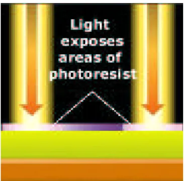
After coating the sample with photoresist, some portions are exposed to ultra violet (UV) radiation. This is the key step in the process; The areas which are exposed and which are unexposed will determine where the final pattern appears. As can be shown in Figure 2.1 The radiation can be any well-collimated radiation
Figure 2.1: Exposure.
source; near-UV photons and electrons are the two most common radiation types. The exposure to the radiation weakens the resist. The areas that are not exposed are not weakened and retain their original cohesion.
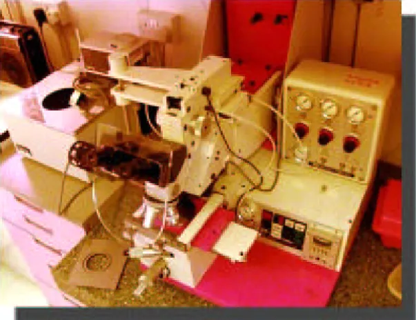
Figure 2.2: Karl Suss Aligner Machine.
2.2.3
Developing Process
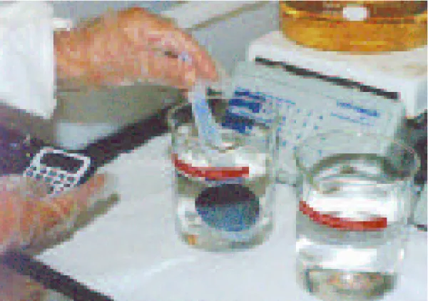
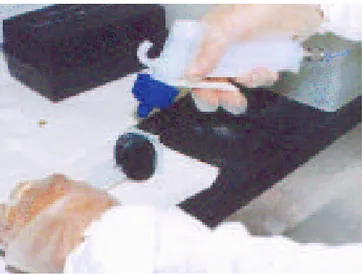
After exposition, the sample is placed in a solvent (dilute NaOH). This solvent is chosen so that it is strong enough to dissolve the weakened (exposed) photoresist, but is not strong enough to affect the unexposed areas. This process which is shown in Figure 2.3 leaves holes in the resist corresponding to the areas that were exposed. after the development process one has to rinse samples in water and then dry them quickly as shown in Figure 2.4.
Figure 2.3: Development Process in Lab.
2.2.4
Etching Process
Wet Chemical Etching
We have a variety of acids, alkalis and oxidising agents, available for wet etching materials. There is also a temperature controlled bath for etches requiring precise temperature control. Table 2.2 gives information on the etchants for various semiconductors and their etch rates. The most important disadvantages of wet chemical etching process is undercutting. Acid is going to eat the substrate not only vertically but also horizontally under the photoresist, which is called undercutting.
Figure 2.4: Drying Process in Lab. Reactive Ion Etching
The RIE system is used to etch features anisotropically (i.e. etching occurs only in the vertical direction with minimal undercutting of the etch mask). Etch gases are admitted into the chamber at low pressure and a radio frequency sig-nal is applied to the parallel electrodes. This breaks up the gas molecules and creates a plasma of reactive chemical species that react with the material be-ing etched (substrate). Gases are chosen that will react with the substrate to produce volatile compounds which are then removed from the etch chamber by the vacuum pumps. The RF signal is applied to the process gases in a manner that causes a voltage difference (bias) between the substrate and the plasma. This voltage accelerates the reactive etch species towards the substrate (called sputtering) and causes etching to occur mainly in the vertical direction. The schematic view of RIE is shown in Figure 2.5.
Etch Mixture Etched Material Etch Rate (approx)
HCl (conc) InP 5-15
HCl (conc) Surface Oxide on GaAs Fast
HCl (conc) InGaAs < 0.02 HCl:H2O (2:1) InP 8 HCl:H2O (1:1) InP 0.7 HCl:H2O (1:2) InP 0.09 H3PO4:HCl (1:1) InP 2.5 H3PO4:HCl (1:2) InP 4.8 H3PO4:HCl (1:3) InP 6.6 H3PO4:HCl (3:1) InP 0.75 H3PO4:H2O2:H2O (3:4:3) GaAs 6
H2O:NH4OH:H2O2 (20:2:1) GaAs 0.5
H2O:NH4OH:H2O2 (100:2:0.7) GaAs 0.1
H2SO4:H2O2:H2O InGaAs 0.5
HBr:CH3COOH:K2Cr2O7 (1:1:1) III-V Compounds 2-5
Br:CH3COOH (1:100) III-V Compounds 1-10
HCl:H2O2:H2O (80:4:1) GaAs 1
Table 2.2: A Guide for Etchants and Their Etch Rates
2.2.5
Deposition Process
After the sample has been developed, it is placed in a deposition chamber and material is deposited. Virtually any material that can be deposited in a dry de-position chamber (sputtering, thermal evaporation, etc.) and many materials can also be deposited in wet chambers (e.g. electrodeposition). The deposited ma-terial covers the entire sample uniformly, covering the holes (where the exposed resist was) and the unexposed resist
2.2.6
Liftoff Process
The final step in the process is to perform a liftoff as can be shown in Figure 2.6 . In this step, the sample is placed in a strong organic solvent that is designed to dissolve the remaining (unexposed) resist. A typical solvent used for this purpose is acetone. When the unexposed resist dissolves, the deposited material that was on top of it peels off the substrate. The material that was deposited
Figure 2.5: Schematic View of the Operation of RIE.
into the holes left by the exposed resist is unaffected. This therefore leaves a pattern of deposited material corresponding to the areas that were exposed to the radiation. For good lift-off we need an undercut in the resist which can be reached by putting the sample into chlorobenzene before the development process for a while. Without putting into chlorobenzene it may not be possible to properly lift-off the resist.
2.3
Exposure Methods
The most important step in the lithographic process is the exposure of the sample to radiation. Only selected areas of the sample are exposed; controlling which areas are exposed and which are not is the central problem in microlithography. In principle, virtually any type of radiation could be used to do the exposure. In practice, there are only two common types; light (ranging from the visible into
or opaque to the radiation that is used. The areas on the sample corresponding to the transparent regions of the mask get exposed and the areas corresponding to the opaque regions is not affected. The beam writing method does not have a physical mask. Here, the radiation source is collimated into a very tightly focussed beam, and the beam is moved across the sample under the control of a computer. The beam exposes the area of the sample that it moves across. Various specific implementations of these techniques are detailed below.
2.3.1
Contact Photolithography
The simplest form of microlithography is known as contact photolithography. Here, a mask is constructed with the desired pattern (exposed areas are trans-parent and unexposed ones are opaque). The mask is then placed directly on top of the substrate, and light is shone down from above. The pattern is then transferred onto the substrate. This is a one-to-one process; the final pattern is exactly the same size as the pattern on the mask. The main advantage of contact lithography is its simplicity. The needed equipment is very simple, little more than the masks and a large UV light. This means that it is easy to do ex-posures on large areas simultaneously. This is the method that is used for large objects that do not need very high resolution features; the traces on a printed circuit board are the most common example. The big disadvantage of contact lithography is that the masks are the same size as the final pattern. This means that the minimum size of the features of the pattern is limited by the resolution of whatever technology created the masks. Simple masks can be made using a laser printer and acetate (transparency) stock; these are usually limited to fea-ture sizes of 200 µm or larger. Higher resolution masks can be made using the techniques discussed below, allowing features of 1µm.
2.3.2
Projection Photolithography
The limitations of contact photolithography make it unsuitable for the manu-facture of integrated circuits, where the typical feature size is in the sub-micron range. Similarly, research into the behavior of small-scale objects needs the ca-pability of constructing sub-micron scale objects in order to approach the ideal of reduced-dimensionality systems. The most common technique for overcoming the limitations of contract lithography is to move the mask away from the sur-face of the sample. In projection photolithography, the mask is moved to near the light source. The presence of the different transparent and opaque regions patterns the light source. This patterned light beam is then passed through a reducer lens, which is focussed on the sample. The reducer acts to decrease the size of the light beam, and hence the size of the pattern. The pattern that is written on the sample is therefore smaller than the pattern that is in the mask. The actual size of the pattern is determined by the reducing factor of the lens, and can be a factor of 10 or more smaller than the mask pattern. Projection photolithography is the most common industrial technique for making integrated circuits. It has several advantages. The chief advantage of the method is that the feature size limitation is determined by the diffraction limit of the light used to make the exposure. For the near-UV light that is common today, features of or-der 0.2 µm can be written. It is also a very fast technique; if the reducing lens has a sufficiently large field of view, an entire wafer can be patterned simultaneously, allowing for high-volume manufacturing. There are, on the other hand, several drawbacks to the projection technique. The most severe problem is that the resolution limit is diffraction-based. This means that if features smaller than the current limit are needed, than it is necessary to move to a system with a shorter
2.3.3
Electron-beam lithography
When we have reached the diffraction limit of light and still want smaller features, there are essentially two options. The first option is to use light with shorter wavelengths. The other possibility is to abandon light entirely and move to a ra-diation type that does not have such severe wavelength limitations. This means using electrons as the radiation source. Unlike the optical methods described above, electron-beam lithography uses a “pencil-beam” approach for writing pat-terns. Instead of using a broad beam of radiation that is physically blocked in some areas by a mask, e-beam systems use a very tightly focussed beam of elec-trons (typically on the order of 50 nm wide) to draw a pattern in the resist. The beam is moved about on the surface by deflection coils; these coils are directly controlled by a computer, which transfers a pattern from memory to the sub-strate. The big advantage of e-beam systems is that they are essentially free of the diffraction limit. A typical e-beam system runs with 20 keV electrons; this corresponds to a wavelength of approximately 0.1 ˚A. The resolution of e-beam systems is therefore limited by other effects; these typically include the physical size of the resist polymer and the size, collimation, and energy of the writing beam. Currently, the best e-beam systems can write features as small as 10 or 20 nanometers, significantly better than the best optical systems. The main problem with electron-beam systems is that they are slow when writing large patterns. Unlike the optical mask methods, where the entire sample is exposed simultaneously, e-beam writers have to draw each element individually onto the substrate. For simple patterns, this is not a severe drawback, but for multi-million transistor microprocessors, this is a major problem. Because of this limitation, e-beam systems are not used in large-scale manufacturing. Instead, they tend to be found in research environments and in industrial prototyping. E-beam writers are also used to manufacture the high-resolution masks used for projection photolithography.
2.4
Future Developments
The current state of the art of microlithography allows for high-speed writing of 0.1 micron object, or for slow writing of objects one tenth that size. There are many ongoing research efforts aiming at improving both numbers; some of the techniques that are being investigated are illustrated here.
2.4.1
X-ray Contact Lithography
With the aid of e-beam lithography, it is now possible to make masks that have feature sizes in the sub-micron range. This makes contact lithography, where the pattern size is identical to the mask size, more attractive. Like projection lithog-raphy, contact lithography is still diffraction limited. However, since the mask is placed directly over the sample, there is no need for any optical elements. This potentially allows contact lithography to be used with much shorter wavelengths, and hence much smaller feature sizes.
The major problem facing contact lithography is the construction of the masks. In order to be competitive with the projection techniques, the contact methods need to be extended into the soft X-ray wavelengths. The mask will therefore need to be opaque to these X-rays. At the same time, the masks need to be as thin as possible; thick masks have severe depth of field problems that reduce the sharpness of the features. Constructing a mask that is opaque to X-rays and is also very thin is a very difficult problem, and is the major limitation in contact lithography systems.
2.4.2
Projection Lithography
The most logical approach for extending the capabilities of lithographic systems is to proceed with standard projection photolithographic systems and move to steadily smaller wavelengths. This has the advantage that there is a large amount of expertise in the construction and operation of projection photolithography sys-tems; in the near term, it is likely that this technique will continue its dominance of the semiconductor industry.
At very short wavelengths, however, problems begin to appear. The mask construction issues discussed above apply with projection systems as well as con-tact systems. In addition, there is the problem that optical lenses lose efficiency at shorter wavelengths. As the wavelength, and hence the feature size, grows smaller, it becomes more difficult to design and build a lens with a large field of view with a homogenous reduction factor. Most of the research into this problem has revolved around using curved mirrors instead of lenses to obtain the pattern reduction.
2.4.3
Electron Projection Lithography
The main problem with electron-beam lithography is not the resolution. The big problem is the speed of the method. Because of the need to draw each individual element, complicated patterns can take a prohibitively long time to complete. The obvious answer is to use a method similar to the optical approaches; a broad beam of electrons patterned by a physical mask. The patterned beam is then reduced down and projected onto the sample. This has the potential of combining the speed of optical lithography with the high resolution of e-beam systems.
The major problem facing electron projection systems is the design of the masks. Unlike photons, electrons are charged, massive particles that carry sig-nificant amounts of energy. The opaque regions of the mask will have to be able to absorb the electrons without significant heating (heating causes ther-mal distortions) and conduct them away in a very short time (on the order of microseconds). The conduction is necessary because of Coulomb interactions be-tween the electrons; if charge builds up on portions of the mask, it will distort the electron beam, and hence the final pattern.
2.4.4
Scanning Probe Lithography
The final method for micromanufacture that is being developed is Scanning Probe Lithography. In this technique, a scanning probe microscope (typically a Scan-ning Tunnelling Microscope, STM) is used to nudge atoms around on a substrate (by applying voltages to very localized areas of the surface). This technique al-lows the construction of objects on an atomic scale. It is extremely slow, and is currently only used for constructing surface-physics model systems, in the same manner Atomic Force Microscopy (AFM) can also be used in lithography for obtaining < 10 nm features.
Mask
Chrome Chrome
Chrome Chrome Chrome
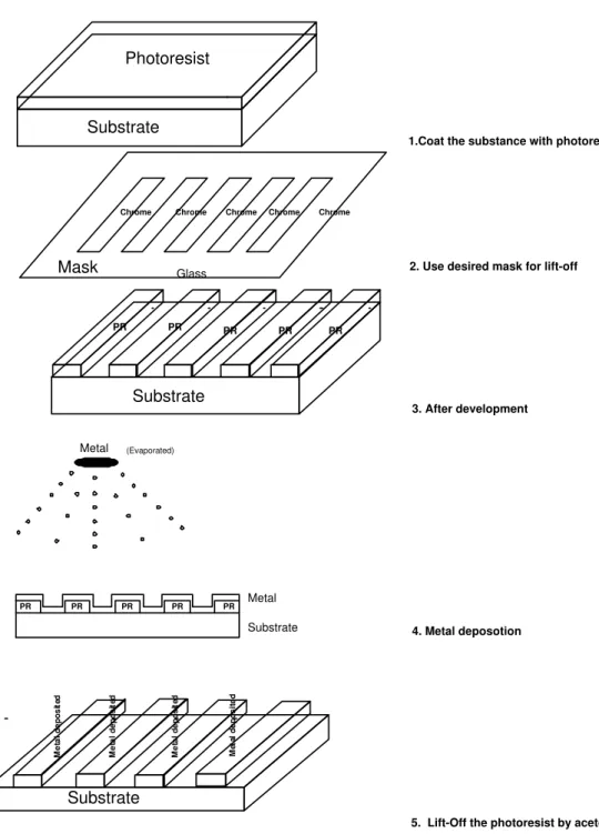
Glass Substrate Photoresist Substrate PR PR PR PR PR Metal (Evaporated)
1.Coat the substance with photoresist
2. Use desired mask for lift-off
3. After development 4. Metal deposotion Substrate Metal PR PR PR PR PR
5. Lift-Off the photoresist by acetone
Substrate M et al d ep os ite d M et al d ep os ite d M et al d ep os ite d M et al d ep os ite d
Chapter 3
Scanning Hall Probe Microscopy
3.1
Hall Effect
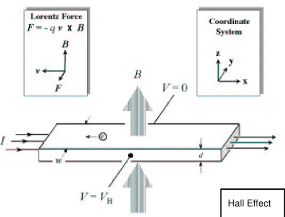
The basic physical principle underlying the Hall effect is the Lorentz force. When an electron moves along a direction perpendicular to an applied magnetic field as shown in Figure 3.1, it experiences a force acting normal to both directions and moves in response to this force and the force affected by the internal electric field. For an n-type, bar-shaped semiconductor shown in Figure 3.1, the carriers are predominately electrons of bulk density n. We assume that a constant current I flows along the x-axis from left to right in the presence of a z-directed magnetic field. Electrons subject to the Lorentz force initially drift away from the current line toward the negative y-axis, resulting in an excess surface electrical charge on the side of the sample. This charge results in the Hall voltage, a potential drop across the two sides of the sample. (Note that the force on holes is toward the same side because of their opposite velocity and positive charge.) This transverse
Hall Effect
Figure 3.1: Hall Effect
density ns = nd, instead of bulk density. One then obtains the equation (3.1) as
ns =
IB e|VH|
(3.1) Thus, by measuring the Hall voltage VH and from the known values of I, B, and q,
one can determine the sheet density nsof charge carriers in semiconductors. If the
measurement apparatus is set up as described later in Section III, the Hall voltage is negative for n-type semiconductors and positive for p-type semiconductors. The sheet resistance ρs of the semiconductor can be conveniently determined by
use of the van der Pauw resistivity measurement technique. Since sheet resistance involves both sheet density and mobility, one can determine the Hall mobility from the equation
µ = |VH| ρsIB
= 1
ensρs
(3.2)
3.1.1
Hall Effect in Inhomogeneous Magnetic Field
In the presence of a magnetic field, the current and electric fiield are not collinear. In the diffusive regime, the constitutive relation between local current and J, electric field E, and external magnetic field B is [14, 18, 19, 21, 22]
J = σE + µH(J × B) (3.3)
where σ is the conductivity, µH is Hall mobility. Solving for J in Equation
3.3gives J = σBE + σBµH(E × B) + σBµ2HB(E · B) (3.4) in which σB = σ 1 + µ2 HB2 (3.5) is the effective conductivity. In the two-dimensional case, E and J are confined within the Hall probe plane (Ez = 0). If the magnetic field is perpendicular to
the Hall plate, i.e., B = Bzz, Equation 3.4 becomesˆ
J = σBE + σBµH(E × Bzz)ˆ (3.6)
within the continuity equation, ∇ · J = 0, and E = −∇φ, we find an equation for the electrical potential. With µHB small and the inhomogeneous effect weak
enough, we neglect terms of order µ2
HBz∇Bz, giving [23]
∇2φ = −µH∇Bz· (∇φ × ˆz) (3.7)
The boundary conditions are: [14, 18] (i)at conducting boundaries, the tangential component of electric field is zero, i.e., ∂φ/∂t = 0; and (ii)at insulating bound-aries, the normal component of current is zero, i.e., ∂φ/∂n − µHBz∂φ/∂t = 0.
the inhomogeneous magnetic field. If we consider a localized flux inside the Hall probe boundary, this term is zero except at the edge of flux. As the gradient in the magnetic field changes direction across the flux, with a constant electric field in this region, the inhomogeneous term is equivalent to an electric dipole source oriented perpendicular to the electric field. [21] This dipole source is the localized Hall response- the local Hall field balancing the Lorentz force. While the magnetic perturbation considered is short range, the potential is affected over large length scales and an average balance results. Since the variation of local electric field is of the order (µHBz)2. Thus in a small uniform magnetic
field (to first order in µHBz), the net Hall electric field can be considered to be
a superposition of these local dipole fields.
3.1.2
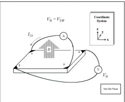
The van der Pauw technique
In order to determine both the mobility µ and the sheet density ns, a combination
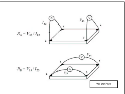
of a resistivity measurement and a Hall measurement is needed. We discuss here the van der Pauw technique which, due to its convenience, is widely used in the semiconductor industry to determine the resistivity of uniform samples [12, 13]. As originally devised by van der Pauw, one uses an arbitrarily shaped (but simply connected, i.e., no holes or nonconducting islands or inclusions), thin-plate sample containing four very small ohmic contacts placed on the periphery (preferably in the corners) of the plate. A schematic of a rectangular van der Pauw configuration is shown in Figure 3.2. The objective of the resistivity measurement is to determine the sheet resistance ρs. Van der Pauw demonstrated
that there are actually two characteristic resistances RAand RB, associated with
the corresponding terminals shown in Figure 3.2. RA and RB are related to the
sheet resistance ρs through the van der Pauw equation
exp−πRA
RS
+ exp−πRB
RS
Van Der Pauw
Figure 3.2: A schematic of a rectangular van der Pauw configuration . which can be solved numerically for ρs. The bulk electrical resistivity ρ can
be calculated using
ρ = ρsd (3.9)
To obtain the two characteristic resistances, one applies a dc current I into contact 1 and out of contact 2 and measures the voltage V43 from contact 4 to
contact 3 as shown in Figure 3.2. Next, one applies the current I into contact 2 and out of contact 3 while measuring the voltage V14 from contact 1 to contact
4. RA and RB are calculated by means of the following expressions:
RA= V43/I12 (3.10)
RB = V14/I23 (3.11)
Van Der Pauw
Figure 3.3: Hall voltage measurement.
can also be used for the Hall measurement. To measure the Hall voltage VH, a
current I is forced through the opposing pair of contacts 1 and 3 and the Hall voltage VH=V24 is measured across the remaining pair of contacts 2 and 4. Once
the Hall voltage VH is acquired, the sheet carrier density ns can be calculated
via the equation
nS =
IB eVH
(3.12) from the known values of I, B and e. There are practical aspects which must be considered when carrying out Hall and resistivity measurements. Primary con-cerns are (1) ohmic contact quality and size, (2) sample uniformity and accurate thickness determination, (3) thermomagnetic effects due to nonuniform temper-ature, and (4) photoconductive and photovoltaic effects which can be minimized by measuring in a dark environment. Also, the sample lateral dimensions must be large compared to the size of the contacts and the sample thickness. Finally, one must accurately measure sample temperature, magnetic field intensity, electrical current, and voltage
3.2
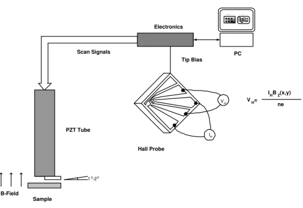
Introduction to Scanning Hall Probe
Mi-croscope
The microscope incorporates a Hall probe which is brought into close proximity with the sample surface by using STM positioning techniques. The hall probe is mounted on the piezotube. The sample is first approached until tunneling is established and then the Hall probe is scanned across the surface to measure the magnetic field and the surface topography simultaneously. Low Temperature Scanning Hall Probe Microscope is composed of four different sections: Air side connections, sample slider, sample holder and the shield. Air side has three lemo connectors, A, B and C for electrical connections. The slider is a piezo driven stick-slip inertial slider, which moves the slider puck along the glass tube. The shield is fitted over the microscope to protect the head from the impacts as it is lowered into the cryostat, as well as sustaining temperature uniformity and electrical shielding.
3.3
Operation
3.3.1
Experimental Details
Hall probes are mounted on to the end of the PZT scanner tube. Extreme care is needed for mounting. Scanning tunnelling microscopy (STM) positioning technique is used for approaching the Hall probe into close proximity with the sample surface. The Hall probe is mounted on the piezotube with a stick-slip coarse approach mechanism and the tilt angle between the Hall probe and the
established and then the Hall probe is scanned across the surface to measure the magnetic field and the surface topography simultaneously as sketched in Figure 3.4. B-Field 10-20 PZT Tube Scan Signals Electronics Hall Probe PC Sample VH= IHBZ(x,y) ne Tip Bias IH Bz (x,y) Z(x,y) VH
Figure 3.4: Schematic diagram of scanning Hall probe microscope .
3.3.2
Sample Mounting
The samples should be glued onto the sample holder with a silver conductive paint and electrical continuity is checked between the sample and sample holders which are shown in Figure 3.5. The holder is then flipped over and fixed to the slider puck with three screws and compression springs. These springs are used to align the sample-Hall probe angle.
Figure 3.5: Hall probe.
3.3.3
Hall Probe Mounting
A low temperature epoxy is used to stick a ceramic part on to the Hall probe holder and Hall probe is also glued to the ceramic part by the aid of the same epoxy. Wire bonder or silver epoxy can be used for electrical bonding. The hall probe must be clean for good contacts. A picture of Scanning Hall Probe Microscope working at low temperature is shown in Figure 3.8, 3.9.
3.3.4
Adjustment of the Hall Probe Angle
The sample should be tilted around 10-1.50 with respect to the Hall probe. This
is achieved by adjusting the three screws used to fix the sample holder to the slider puck. The alignment is done under an optical microscope.
Tip
VH+
V
H-IH+
I
H-Figure 3.6: Hall probe connections.
3.3.5
Final Adjustment
After getting quite close under the optical microscope, the slider puck is backed around 50-70 steps. Then the shield is put on very gently and the LT-SHPM is lowered into the cryostat carefully, trying not to touch it to the walls. There is a teflon centering ring which will minimize this effect.
3.3.6
Preparing for Cool Down
The sample space has to be pumped to 10−6 mbar range and flushed with pure
He gas several times (3-4) and left with He gas before cooling the system down while the LT-SHPM electronics is turned off. The LT-SHPM should be cooled down or warmed up with a maximum rate of 2-3 K/min. Higher rates can cause damage in time.
Figure 3.7: Scanning Hall Probe Microscope working at room temperature.
3.4
LT-SHPM Control Electronics and
Soft-ware
Figure 3.8: Low Temperature Scanning Hall Probe Microscope.
Figure 3.9: Low temperature scanning Hall probe microscope head.
3.4.1
Power Supply
This card generates all the relevant regulated voltages for the box (+220V, -220V, +15V, -15V, +8V, -8V, +420V).
3.4.2
Scan Dac
Sample
Hall Probe Bonding Wire
1o-1.5o
Figure 3.10: Adjustment of Hall probe angle.
3.4.3
HV Amplifier
This card combines and amplifies x, y scan voltages (from scan Dac card) with z-voltage and generates N, S, E and W voltages to derive the scan PZT.
3.4.4
DAC Card
This card has four 16 bit DACs which supplies Vbias, Zof f set, Vcoil and Itunnel−set
for the controller. Output range of this voltages can be selected by jumpers on the card, ±10 V, ±5 V and ±2.5 V. The coil voltage output can supply up to
±250 mA to drive a small test coil directly.
3.4.5
Slider card
This is used to drive the x, y, z sliders. It generates a special voltage pulse applied to the relevant electrodes under software or keyboard control. Each slider pulse
3.4.6
AD Converter Card
This card is used to read all the relevant voltages using a 200 kHz, programmable gain(1, 2, 4, 8), 8 channel analog to digital converter and facilities data interface with the computer.
3.4.7
Controller Card
This card achieves tunnelling feedback and keeps tunnel current constant by adjusting the tip-sample separation. There is a -100 mV/nA gain current to voltage converter at the electronic box attached to the head. Output of this I-V converter should be connected to Itip input of the card.
3.4.8
Hall Probe Amplifier Card
The IHall is generated and VHall is processed by this card. The Hall current
can be switched on (LED is lit) under software control, when switched off, the current leads are short-circuited to each other.
3.5
Images from Scanning Hall Probe
Micro-scope at RT and LT
Surface magnetic fields at nanometre scale can be seen in Figure 3.11 by scanning a nanofabricated Hall probe accross the sample to obtain quantitative image of surface magnetic field. Magnetic domains at nanometer scale obtained by Prof. Adarsh Sandhu is shown in Figure 3.11. Image of Vortices trapped in YBCO thin film at 77 K obtained [20] with SHPM is shown in Figure 3.12 .
Chapter 4
Hall Probe Manufacturing on
GaAs and InSb
4.1
Manufacturing Process
Manufacturing Hall probes on various materials such as GaAs, InSb, Bi is one of the most important part of scanning Hall probe microscopy, after designing the desired patterns on our masks, it is possible to produce our Hall probes in the Bilkent Class-100 clean-room by photolithographic processes. The steps needed for the production of the probes can be seen in Figure 4.1. In each step extreme care is needed. You can see this process steps on one Hall probe in Figure 4.2
4.1.1
Hall Probe Etch
The heart of probe manufacturing is the Hall probe etch. The resist is spun and then the pattern is exposed with Karl Suss Aligner. Our resist thickness directly affect the time needed for exposure. After exposition we develop our sample in developer which is used to remove the resist exposed under UV. Seconds in
Photolithographic process for Hall probe
Hall Probe Etch
Deep Etch Recess etch Ohmic Contact
Tip Metalization
Figure 4.1: Photolithographic Process for Hall Probe Manufacturing . developing procedure can be significant, developing the resist 2-3 seconds more can cause under-etch problems for the resist and developing the resist 2-3 seconds less can result in undeveloped photoresist in Hall part. After developing one should not forget to look the samples under optical microscope. If one gets a good pattern 1 micron Hall probe sample is etched in a suitable acid such as sulfuric acid for GaAs for a few seconds according to your needs for etch height. The height of the photoresist before wet-etch and after wet-etch is measured by Dek-dak profiler. The difference gives you how much you etch your sample.
Deep Etch
4 Hall probe on the chip Tip Metalization Ohmic Contacts
E-Beam Lit.
Deep Etch
Figure 4.2: Process steps on o the Hall probe .
4.1.3
Recess Etch
The Hall probes must be lowered on to the sample within a few microns to get a high resolution in magnetic topography of the sample. Bonding from the Hall fingers to Hall probe holder cause a problem: the bonding wire can touch the sample while lowering your Hall probe. Etching the Hall Probe by a square mask 50-60 microns from sides is the best solution for this problem.
4.1.4
Ohmic Metalization
Ohmic contact can be obtained after this process which is shown in Figure 4.3. After spun the resist, it is exposed in Karl Suss aligner. The sample is soaked in Chlorobenzene for a while before develop the resist. Chlorobenzene is used for good lift-off. Then the sample is loaded into box-coater for metallization (Ti/Ge/Ti/Au). After metallization acetone is used for lift-off. The contacts are
4.1.5
Tip Metalization
After spinning the resist, it is exposed in Karl Suss aligner. Chlorobenzen is used for good lift-off. Now you can use box-coater for metallization (Ti/Au). After metallization acetone is used for lift-off.
4.1.6
Hall Probes manufactured on GaAs/AlGaAs 2DEG
A top view of a Hall probe manufactured on GaAs/AlGaAs [25, 26] (n2D =
2.7 × 1011 cm−2, µ = 300000cm2/V s at 4.2 K) is shown in Figure 4.3. A single
picture of a 1 micron Hall probe manufactured on GaAs is shown in Figure 4.3 You can see only four chips manufactured on GaAs from the totally 20 chips
Figure 4.4: Four manufactured Hall probe chips on GaAs. .
4.1.7
Hall Probes manufactured on InSb
You can see the images of Hall probes manufactured on InSb with the following specifications. ns = 2.0 × 1012cm−2 and µ = 55500cm2V−1s−1 at room
InSb ~1 micron GaAs (100) ~350 micron
ns=2 x1012 cm-2
Chapter 5
Grating Manufacturing on
Mechanical GaAs and NiFe
Materials
5.1
Grating Structure
The mechanical gratings are manufactured for calibration of our SHPM. NiFe gratings are manufactured to be used in magnetic imaging in the future. 10 nm Ti and 100 nm NiFe materials deposited on a mechanical GaAs. By using square, rectangular masks square and rectangular photoresists have been formed on the surface of GaAs. HN O3 and HF are used in the etch process. The sample is
deep etched approximately 110nm. Finally the sample completely coated with 10 nm Ti and 50 nm Au as can be seen in Figure 5.1.
100 A Ti +50 nm Au
Mechanical GaAs 100 A Ti
100 nm NiFe GaAs
Fig1.4 Grating Structure
SHPM Group
Figure 5.1: Grating Structure.
5.2
Rectangular gratings on NiFe
Rectangular gratings are manufactured on NiFe materials which has the dimen-sions of 6 microns to 30 microns as can be seen in Figure 5.2. The details of process is completely shown in Figure 5.1 Square gratings are manufactured on NiFe materials which have the dimensions of 10 microns to 10 microns as can be seen in Figure 5.4. The process is shown in Figure 5.1 Various gratings are manufactured on NiFe materials which have the dimensions of 2 microns to 30 microns that can be seen in Figure 5.5. The process is completely shown in
100 A0 Ti +50 nm Au
A.Oral & M.Kaval Fig 1.5 Rectangular Grating (6 * 30 microns side)
SHPM Group
30 micron
6 micron Mechanical GaAs
100 A0 Ti 100 nm NiFe
GaAs
Figure 5.2: Rectangular gratings manufactured on NiFe material .
The image of rectangular gratings before coated with Gold can be seen in Figure 5.3. The blue parts are mechanical GaAs.
30 micron
6 micron
SHPM Group
100 A0 Ti
500 A0 NiFe
Fig 1.6 Square Grating (10micron*10 micron)
SHPM Group10 micron
10 micron
6 micron 4 micron 10 micron 8 micron 10 micron 2 micron
Figure 5.6: 2 micron period 2D circular grating obtained with Tuning fork AFM at room temperature.
Chapter 6
Results
6.1
BH Curves of GaAs Hall Probes
The characteristics of three manufactured GaAs Hall probes at IH=20µA is
Figure 6.2: M32-1 GaAs Hall Probe
6.2
BH Curves of InSb Hall Probes
The characteristics of three manufactured InSb Hall probes at IH=20, 50, 100µA
is shown in Figure 6.5, 6.7, 6.6, 6.10, 6.8, 6.9
6.3
Images taken by LT-SHPM and by STM
mode
After obtaining our LT-SHPM it has been tested at room temperature (300 K) and at 77 K with the aid of a cryostat. Low temperature scanning Hall probe microscope has been scanned over the gratings (1µm) in STM mode with the aid of platinum tip. The images obtained from the scan is shown in Figure 6.11 and 6.12 Secondly, the microscope has been tested at room temperature (RT) as a Scanning Hall probe microscope. The images of magnetic disc obtained from the American National Institute of Standards and Technology (NIST) is shown in Figure 6.12 and 6.11.
Figure 6.3: M32-2 GaAs Hall Probe
6.4
Manufactured InSb HP characteristics on
single garnet crystal
The manufactured InSb Hall Probes are scanned over single crystal garnet, with a scan size of 25µm×25µm. The first images have been obtained by Prof. Adarsh Sandhu and Hiroshi Masuda in Japan. The images were in Figure 6.13 obtained while approaching to the surface with a Hall current of 9 µA. For higher values of Hall current 12 µA and 15 µA the images in Figure 6.14 were obtained.
Figure 6.4: M34 GaAs Hall Probe
Figure 6.8: InSb9 − 10 Hall Probe
Figure 6.10: InSb7 − 100 Hall Probe
Figure 6.12: (a).Magnetic field image 78 Gauss × 50 µm × 50 µm, images of magnetic field (b) STM Topography 120 nm × 7.9 µm × 7.9 µm of NIST MFM Reference sample obtained at T=100 K
A. B. C.
Figure 6.13: SHPM images of Garnet film obtained with InSb HP A. IH=9 µA,
D. E. F.
Figure 6.14: Images of Garnet film obtained with InSb HP D. IH=12 µA,
Chapter 7
Conclusions
In this thesis manufacturing of Hall probes of 1 micron size size on GaAs and InSb materials to be used in scanning Hall probe microscopy for magnetic imaging at nanometer scale has been described in detail. Nearly 45 Hall probe were manufactured to be used in magnetic imaging. First images obtained by our SHPM at room temperature can be seen in Figure 6.11, 6.12. On the other hand, you can see the images obtained by manufactured InSb Hall probes in Figure 6.13 and 6.14 obtained by our collaborator in Japan. As a suggestion for future work by using our new cryostat which can operate between 1.5 K and 300 K, we can be able to take the images of vortices of high Tc superconductive
materials such as YBCO. It is going to be possible for us to fabricate submicron Hall probes by using electron beam lithography which can be used to increase the lateral resolution in magnetic imaging. Finally by using different materials such as Bismuth for Hall probe manufacturing it can be possible for us to increase the lateral magnetic resolution further.
Bibliography
[1] P. Weiss. L’hypth`ese du champs mol´eculaire et la propri´et´e ferromagn´etique. J. de Phys. 6, 661-690, (1907).
[2] L. v. H´amod and P. A. Thiessen. ¨uber die Sichtbarmachung von Bezirken
verschieden ferromagnetischen Zustandes fester K¨orper. Z. Phys., 71,
442-444,(1931).
[3] On inhonogenities in the magnetization of ferromagnetic materials. Phys. Rev., 38:1903-1905,1931.
[4] A. L. Schawlow, B. T. Matthias, H. W. Lewis, and G. E. Delvin. Structure of
the intermediate state in superconductors. Phys .Rev., 95, 1344-1345, 1954.
[5] L. N. Vu, M. S. Wistrom, and D. J. Vanharkingen, Physica B 194, 1791 (1994).
[6] Y. Martin, D.Rugar, and H. K. Wickramasinghe. High-resolution magnetic
imaging of domains in TbFe by force microscopy. Appl. Phys. Lett. 52, 244
(1988).
[7] A. Moser, H. J. Hug, I. Parashikov, B. Stiefel, O. Fritz, H. Thomas, A. Baratoff, H. J. Guntherodt, and P. Chaudhari. Observation of Single
Vor-[8] Y. Matsuda, A. Fukuhara, T. Yoshioka, S. Hasegawa, A. Tonomura, and Q. Ru, Phys. Rev. Lett. Computer reconstruction from electron holograms and
observation of flux on dynamics. 66, 457 (1991).
[9] A. Oral, J. C. Barnard, S. J. Bending, I. I. Kaya, S. Ooi, T. Tamegai, M. Henini. Direct Observation of Melting of the Vortex Solid in
Bi2Sr2CaCu2O8+δ Single Crystals Phys. Rev. Lett. 80 , 16 (1998)
[10] A. M. Chang, H. D. Hallen, L. Harriot, H. F. Hess, H. L. Loa, J. Kao, R. E. Miller, and T. Y. Chang, Appl. Phys. Lett. Scanning Hall probe microscopy. 61, 1974 (1992).
[11] T. schweinb¨ock, D. Weiss, M. Lipinski and K. Eberl. Scanning Hall probe
microscopy with shear force distance control. Appl. Phys. Lett. 87, 6496
(2000).
[12] L. J. van der Pauw, A Method Measuring Specific Resistivity and Hall Effect
of Discs of Arbitrary Shapes Philips Res. Reports 13, 1-9(1958).
[13] L. J. van der Pauw, A Method Measuring Specific Resistvity and Hall
Co-efficient of Lamellae of Arbitrary Shape, Philips Tech. Review 20,
220-224(1958).
[14] R. S. Popovic, Hall effect Devices (Adam Hilger, Bristol, 1991)
[15] A. N. Grigorenko, S. J. Bending, J. K. Gregory, R. G. Humphreys.
Scan-ning Hall probe microscopy of flux penetration into a superconducting Y Ba2Cu3O7−δ thin film strip Appl. Phys. Lett. 78, 11 2001
[16] A. Oral, J. C. Barnard, S. J. Bending, S. Ooi, H. Taoka, T. Tamegai, M. Henini. Disorder-driven intermediate state in the lattice melting transition
of Bi2Sr2CaCu2O8+δ single crystals. Phys. Rev. B, 56, 22 (1997)
[17] S. J. Bending, A. N. Grigorenko, R. G. Humphreys, M. J. Van Bael, J. Bekaert, L. Van Look, V. V. Moshchalkov, Y. Bruynseraede. Scanning Hall
Probe Microscopy of Nanostructured Superconductors Physica C, 341 − 348
(2000) 981-984
[18] G. De Mey, Adv. Electron. Electron Phys. 61, 1 (1983) [19] A. W. Baird, IEEE Trans. Magn. MAG 15, 1138 (1979).
[20] A. Oral, S. J. Bending, M. Henini. Scanning Hall probe microscopy of
su-perconductors and magnetic materials. J. Vac. Sci. Technol. B 14, 2 (1996)
[21] I. Hlasnik and J. Kokovec, Solid State Electron. 9, 585 (1966).
[22] A. Nathan, W. Allegretto, H. P. Baltes, and Y. Sugiyama, IEEE Trans. Electron Devices ED − 34, 2077 (1987).
[23] S. J. Bending and A.Oral, J. Appl. Phys. 81, 3721 (1997)
[24] A. Oral and S. J. Bending, M. Henini. Real-Time scanning Hall probe
mi-croscopy. Appl. Phys. Lett. 69, 9 (1996)
[25] Adarsh Sandhu, Hiroshi Masuda, Ahmet Oral and Simon. J. Bending. Room
temperature magnetic imaging of magnetic storage media and garnet epilay-ers in the presence of external magnetic fields using a sub-micron GaAs SHPM J. of Crystal Growth 227 − 228, 899-905 (2001)
[26] Adarsh Sandhu, Hiroshi Masuda, Ahmet Oral and Simon. J. Bending. Room
temperature Sub-micron Magnetic imaging by Scanning Hall Probe Micro-scope, J. Appl. Phys. 40, 4321-4324 (2001)