Fabrication of AlN/BN bishell hollow nanofibers by electrospinning and atomic layer
deposition
Ali Haider, Cagla Ozgit-Akgun, Fatma Kayaci, Ali Kemal Okyay, Tamer Uyar, and Necmi Biyikli
Citation: APL Materials 2, 096109 (2014); doi: 10.1063/1.4894782
View online: http://dx.doi.org/10.1063/1.4894782
View Table of Contents: http://scitation.aip.org/content/aip/journal/aplmater/2/9?ver=pdfcov Published by the AIP Publishing
Articles you may be interested in
Tuning the oxidation states and crystallinity of copper oxide nanofibers by calcination J. Vac. Sci. Technol. B 32, 04E104 (2014); 10.1116/1.4874617
Fabrication of p-type ZnO nanofibers by electrospinning for field-effect and rectifying devices Appl. Phys. Lett. 104, 042105 (2014); 10.1063/1.4863409
Characterization of hollow BaTiO3 nanofibers and intense visible photoluminescence J. Appl. Phys. 114, 134303 (2013); 10.1063/1.4823988
Vanadium pentoxide nanotubes by eelectrospinning AIP Conf. Proc. 1502, 398 (2012); 10.1063/1.4769159
Synthesis of palladium-doped silica nanofibers by sol-gel reaction and electrospinning process AIP Conf. Proc. 1455, 109 (2012); 10.1063/1.4732478
APL MATERIALS 2, 096109 (2014)
Fabrication of AlN/BN bishell hollow nanofibers by
electrospinning and atomic layer deposition
Ali Haider,1,2Cagla Ozgit-Akgun,1Fatma Kayaci,1,2Ali Kemal Okyay,1,2,3 Tamer Uyar,1,2and Necmi Biyikli1,2,a
1National Nanotechnology Research Center (UNAM), Bilkent University, Bilkent, Ankara 06800, Turkey
2Institute of Materials Science and Nanotechnology, Bilkent University, Bilkent, Ankara 06800, Turkey
3Department of Electrical and Electronics Engineering, Bilkent University, Bilkent, Ankara 06800, Turkey
(Received 4 July 2014; accepted 26 August 2014; published online 8 September 2014)
Aluminum nitride (AlN)/boron nitride (BN) bishell hollow nanofibers (HNFs) have been fabricated by successive atomic layer deposition (ALD) of AlN and sequen-tial chemical vapor deposition (CVD) of BN on electrospun polymeric nanofibrous template. A four-step fabrication process was utilized: (i) fabrication of polymeric (nylon 6,6) nanofibers via electrospinning, (ii) hollow cathode plasma-assisted ALD of AlN at 100◦C onto electrospun polymeric nanofibers, (iii) calcination at 500◦C for 2 h in order to remove the polymeric template, and (iv) sequential CVD growth of BN at 450◦C. AlN/BN HNFs have been characterized for their chemical compo-sition, surface morphology, crystal structure, and internal nanostructure using X-ray photoelectron spectroscopy, scanning electron microscopy, transmission electron mi-croscopy, energy dispersive X-ray spectroscopy, and selected area electron diffrac-tion. Measurements confirmed the presence of crystalline hexagonal BN and AlN within the three dimensional (3D) network of bishell HNFs with relatively low im-purity content. In contrast to the smooth surface of the inner AlN layer, outer BN coating showed a highly rough 3D morphology in the form of BN nano-needle crystallites. It is shown that the combination of electrospinning and plasma-assisted low-temperature ALD/CVD can produce highly controlled multi-layered bishell ni-tride ceramic hollow nanostructures. While electrospinning enables easy fabrication of nanofibrous template, self-limiting reactions of plasma-assisted ALD and sequen-tial CVD provide control over the wall thicknesses of AlN and BN layers with sub-nanometer accuracy. © 2014 Author(s). All article content, except where
other-wise noted, is licensed under a Creative Commons Attribution 3.0 Unported License.
[http://dx.doi.org/10.1063/1.4894782]
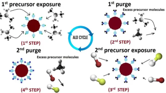
Recent technological developments for creation of novel nano structured materials have pro-moted the control over structure, composition, and uniformity of nanomaterials. Two important approaches of nanofabrication are known as “top down” and “bottom up”.1Bottom up approaches are gradually gaining superiority over top down approaches due to physical limitations associated with top down approaches as described by Moore’s law. As bottom up strategies, chemical vapor deposition (CVD), atomic layer deposition (ALD), molecular beam epitaxy (MBE), self-assembled monolayer (SAM) method, Langmuir Blodgett (LB) technique, and layer-by-layer (LbL) assembly have been widely used which provide fabrication of controlled layered structures from various kinds of materials.2–5Among them, ALD is a special CVD technique in which the substrate is exposed to two alternating precursors in sequential steps separated by inert gas purges. Figure1shows a
aAuthor to whom correspondence should be addressed. Electronic mail:[email protected]
096109-2 Haideret al. APL Mater. 2, 096109 (2014)
FIG. 1. Schematic representation of an ALD cycle consisting of the following steps: (i) exposure of first precursor, precursor absorbs on reactive sites and reaction products are formed, (ii) purge to evacuate the reactor from unreacted excess precursor molecules and gaseous reaction by-products, (iii) exposure of second precursor, which reacts with the adsorbate to form a monolayer of desired material, (iv) purge to remove unreacted precursor molecules and by-products of the reaction.
schematic representation of a typical ALD cycle. As precursor molecules are exposed separately, each ALD cycle results in a monomolecular layer of the given precursor, which eventually becomes independent of the precursor exposure after saturation of the reactive surface sites. Therefore, ALD has the advantage of layer-by-layer self-limiting and ultimate conformal growth on high aspect ratio structures. These distinct advantages make ALD a promising alternative method for the synthesis of nanostructures using template-based methods.6Furthermore, a high degree of synthetic control can be achieved by performing fabrication on pre-existing nanostructured templates.7,8
Being members of the III-nitride family, aluminum nitride (AlN) and boron nitride (BN) have similar lattice parameters and are known for their distinctive material properties, including wide band gap, high-temperature stability, high oxidation and corrosion resistance, as well as high thermal conductivity. Nanostructured AlN have emerged as a promising candidate for high-surface area and highly sensitive biological and chemical sensors.9,10Mostly tubular AlN nanostructures have been synthesized at high temperatures using template-free methods.11–13 Recently, Ozgit-Akgun
et al. have reported template-based synthesis of AlN hollow nanofibers (HNFs) at temperatures as
low as 200◦C using a combination of electrospinning and plasma-assisted atomic layer deposition (PA-ALD).14
BN and BN nanotubes (BNNTs) are structural analogues of carbon and carbon nanotubes (CNTs), respectively. BN can exist in various forms such as rhombohedral (r-BN), hexagonal (h-BN), cubic (c-BN), turbostratic (t-BN), and amorphous (a-BN).15–17 In contrast to metallic or semiconducting CNTs, BNNTs exhibit band gap values of∼5.5 eV, which is found to be indepen-dent of tube chirality and morphology.18Primarily, the interest in BNNTs arose due to a recognized fact that layered BN structure is much more thermally and chemically stable than graphite carbon structure.19Moreover, it has been demonstrated that BNNTs exhibit considerably improved thermal and chemical stabilities than CNTs.20With these inherited properties in BN tubular nanostructures, researchers have shown BNNTs applications in composite reinforcement,21gas adsorption,22 mem-brane filters,23field emitters,24and UV emission.25BNNTs have been synthesized previously by arc discharge, laser ablation, and high-temperature CVD methods.25 Important constraints associated with the previous methods of fabrication are severe preparation conditions, limited control over morphology, and low purity of the resulting BNNTs.25
Electrospun polymeric nanofibers can be utilized as sacrificial templates owing to their design flexibility and low production cost.14These polymeric nanofiber templates offer unique capabilities
096109-3 Haideret al. APL Mater. 2, 096109 (2014)
for producing nanofibers of uniform diameters. Various kinds of 1D fibrous polymer structures in the range of few micrometers to few hundred nanometers can be obtained via electrospinning.26–28 Researchers have fabricated hafnia (HfO2),29zinc oxide (ZnO),30and alumina (Al2O3)31 HNFs by combining ALD and electrospinning processes. HNF synthesis by ALD using electrospun nanofiber templates is a rather simple and effective way to control the properties of resulting nanofibers. Recently, we have developed hollow cathode plasma-assisted ALD (HCPA-ALD) recipes for de-positing thin films of III-nitrides and their alloys with low impurity content.32 Here, we report structural, morphological, and compositional properties of AlN/BN bishell HNFs fabricated via suc-cessive combination of HCPA-ALD and sequential plasma-assisted CVD on electrospun polymeric nanofibers.
A four-step fabrication process was utilized to fabricate the AlN/BN HNFs. First, nylon 6,6 nanofibrous template was prepared by electrospinning. Then, AlN growth was carried out on elec-trospun polymeric nanofibrous template using alternating exposures of trimethylaluminum (TMA) and nitrogen/hydrogen (N2/H2) plasma as aluminum and nitrogen precursors, respectively. After that, AlN HNFs have been obtained by removing the core polymeric template by calcination. As a last step, BN has been deposited on AlN HNFs using triethylboron (TEB) and N2/H2 plasma as alternating precursors for boron and nitrogen to obtain AlN/BN bishell HNFs. The deposition temperature of BN (450◦C) was not suitable for preserving the structure of polymeric templates, as polymer degradation starts around 350◦C.33,34 This compatibility issue was overcome by first depositing a layer of AlN at 100◦C, followed by a calcination process at 500◦C to efficiently remove the polymeric core, and finally BN deposition at 450◦C.
Electrospinning of polymeric nanofibers: Nylon 6,6 having 8 wt.% (w/v) was dissolved in
formic acid by stirring for 3 h at room temperature, for each sample. The resulting homogeneous clear solution was placed in 10 ml syringes fitted with metallic needles having inner diameter of 0.8 mm. The syringes were fixed horizontally on the syringe pump (Model: SP 101IZ, WPI). The polymer solution was pumped with feed rate of 1 ml/h during electrospinning and the tip-to-collector distance was set to 10 cm. 15 kV was applied to the metal needle tip using high voltage power supply (Matsusada, AU Series) for the electrospinning of the polymer solution. The solvent evaporated on the way to the grounded stationary cylindrical metal collector (height: 15 cm, diameter: 9 cm) covered with a piece of aluminum foil. The randomly oriented electrospun nylon nanofibers were deposited onto Si wafer which was fixed on the aluminum foil. The electrospinning setup was enclosed in a Plexiglas box and the electrospinning was carried out at 23◦C and 36% relative humidity.
Atomic layer deposition of AlN: A 200 cycle ALD growth of AlN was carried out on
elec-trospun nanofibers at 100◦C in a Fiji F200-LL ALD reactor (Ultratech/Cambridge Nanotech Inc.), which is equipped with a stainless steel hollow cathode plasma source (Meaglow Ltd.), with a base pressure of 150 mTorr. Precursors utilized for the growth of AlN were TMA and N2/H2plasma with argon (Ar) as the carrier and purge gas. One HCPA-ALD cycle consisted of 0.06 s TMA pulse/10 s Ar purge/40 s N2/H2plasma (50/50 sccm, 300 W)/10 s Ar purge. AlN growth was followed by the calcination of AlN-coated nylon nanofibers in air ambient at 500◦C for 2 h in order to thermally decompose the polymeric core.
Low-temperature sequential CVD of BN: Following the calcination of AlN-coated polymeric
nanofibers, AlN HNFs were introduced into the same ALD reactor and coated with BN at 450◦C to obtain AlN/BN bishell HNFs. 1000 growth cycles of BN were carried out utilizing TEB and N2/H2 plasma sequentially as boron and nitrogen precursors with Ar as carrier and purge gas. One growth cycle consisted of 0.12 s TEB pulse/20 s Ar purge/40 s N2/H2 plasma (50/50 sccm, 300 W)/20 s Ar purge. Precursor and plasma carrier gas flow rates were 30 and 100 sccm, respectively. Samples were taken out from the reactor through a load-lock and exposed to air as soon as the ALD reactor cooled down to 200◦C. The reason why this growth step is defined as sequential CVD instead of ALD stems from the experimental evidence based on X-ray photoelectron spectroscopy (XPS) studies confirming that TEB decomposition initiates at temperatures above 350◦C.35Due to precursor decomposition, film growth is decomposition-limited which deviates from the ideal self-limiting ALD growth character and gas-phase CVD reactions start to occur which leads to precursor dose-dependent non-saturating growth behavior. Within the CVD regime, a growth temperature of
096109-4 Haideret al. APL Mater. 2, 096109 (2014)
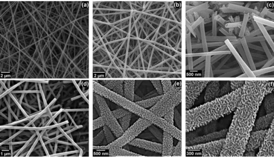
FIG. 2. (a) Representative SEM images of electrospun nylon 6,6 nanofibrous template having an average fiber diameter of ∼100 nm. (b) and (c) Representative SEM images of AlN HNFs synthesized by depositing 200 growth cycles of AlN on polymeric nanofibrous template at 100◦C and then calcinated at 500◦C for 2 h in air. (d) Representative SEM image of AlN/BN bishell HNFs obtained after depositing BN on AlN HNFs template. (e) and (f) Magnified SEM images revealing the surface morphology of AlN/BN bishell HNFs.
450◦C is selected, as reasonable growth per cycle (GPC) values were only observed at temperatures above 350◦C.35
Compositional and structural characterization: Scanning electron microscopy (SEM)
anal-yses were carried out using Quanta 200 FEG SEM (FEI). Prior to SEM imaging, samples were coated with∼5 nm Au/Pd alloy. Transmission electron microscopy (TEM), energy dispersive X-ray spectroscopy (EDX), and selected area electron diffraction (SAED) analyses were performed using a Tecnai G2 F30 transmission electron microscope (FEI). TEM samples were prepared by scratching hollow nanofibers from the substrate and dispersing them into ethanol, followed by sonification and drop casting onto copper grids. Grazing-incidence X-ray diffraction (GIXRD) measurements of corresponding BN thin film were performed in a PANalytical X’Pert PRO materials research diffractometer using Cu Kα radiation. In order to obtain information from very thin layers, GIXRD is preferred. GIXRD measurements are taken at very small incidence angles (typically smaller than 0.5◦), which enables the small penetration depths and intensity enhancement at the surface. Chemical composition and bonding states were investigated by XPS using K-Alpha spectrometer (Thermo Fisher Scientific) with a monochromatized Al Kα X-ray source.
Electrospun nylon polymeric nanofibers have been used as templates for the fabrication of AlN/BN bishell nanofibers. SEM images of electrospun nanofibers are shown in Fig.2(a), which reveals the smooth morphology of nanofibers with relatively uniform diameters. The average fiber diameter of electrospun nanofibers was measured as ∼100 nm. AlN has been deposited using HCPA-ALD, where appropriate wall thickness has been achieved by 200 growth cycles. AlN coated electrospun polymeric nanofibers were calcined at 500◦C for 2 h in air ambient in order to remove polymeric core. Figures 2(b)and 2(c) show the SEM images of AlN HNFs synthesized by the deposition of 200 cycles AlN on polymeric nanofibrous template. The morphology of AlN HNFs is highly conformal and uniform by virtue of self-terminating chemical reactions of HCPA-ALD. These AlN HNFs are ideal replicas of electrospun nanofibers with hollow morphology.
1000 cycles of BN growth were carried out at 450◦C on AlN HNFs to obtain AlN/BN bishell HNFs. Figures2(d)–2(f)depict SEM images of AlN/BN bishell HNFs obtained after depositing BN on AlN HNFs originally based on electrospun polymeric template. SEM images reveal that integrity of the fibrous structure was preserved after BN deposition and 3D network of AlN/BN bishell HNFs have been successfully obtained. Figures2(e)and2(f)represent the high magnification SEM images
096109-5 Haideret al. APL Mater. 2, 096109 (2014)
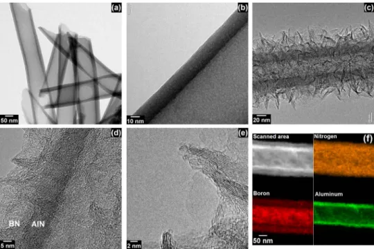
FIG. 3. (a) and (b) Representative bright field TEM images of AlN HNFs. (c) and (d) Representative bright field TEM images of AlN/BN bishell HNF having an average inner fiber diameter of∼100 nm with an average wall thickness of ∼20 nm and ∼35 nm of AlN and BN, respectively. (e) Representative HR-TEM image of AlN/BN bishell HNF. (f) EDX elemental map of aluminum, boron, and nitrogen from an individual AlN/BN HNF.
of AlN/BN bishell HNFs, which reveal that the surface of AlN/BN HNFs is not smooth; instead a highly rough, compact, and curly surface morphology has been obtained. These SEM images show a branching feature with peculiar 3D nanostructures. Currently, presence of this branching feature is not well understood. However, one possible mechanism is that, abundant growth vapors in CVD mode may have created new growth steps on the preceding BN nanosheets which could have resulted in outgrowth of this 3D branched structure. This repetitive branched structure might have terminated upon colliding with other branches of this structure, which is reported in literature as well.36
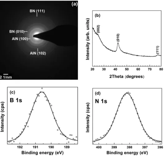
Before calcination process, polymer core was clearly observed in AlN coated templates.37AlN coated polymeric nanofibers were calcined at 500◦C for 2 h in order to obtain AlN HNFs which have been presented in Figs.3(a)and3(b). Wall thickness of AlN was measured as∼20 nm, which is highly conformal and uniform. Figures3(c)–3(e)show TEM images of AlN/BN bishell HNFs. BN radially grows on the surface of AlN and surface of BN is terminated by highly rough nanoneedle like morphology. The average thickness of BN nanoneedle terminated layer is∼35 nm, obtained after carrying out 1000 growth cycles of BN on AlN HNFs. Bishell hollow structure with separate AlN and BN layers can be clearly observed. Lattice fringes corresponding to different crystallographic planes of BN can be observed in high-resolution TEM image [Fig.3(e)], which reveals that BN has a polycrystalline layered structure. Figure3(f)shows EDX elemental mapping of boron, aluminum, and nitrogen from an individual AlN/BN HNF. The distribution of elements is clarified by selecting a cross-sectional portion in the specimen and rastering the electron beam point by point over the selected portion of interest. The colored maps show strong contrast among boron, aluminum, and nitrogen, and they reveal the elemental distribution along the scanned area. Nitrogen and boron are uniformly distributed along the scanned area while uniform aluminum distribution can be seen at the inner shell of the hollow nanofiber. It confirms the successful formation of AlN/BN bishell hollow nanofiber networks with a distinct interface between AlN and BN. SAED pattern of AlN/BN HNFs [Fig.4(a)] exhibited several polycrystalline diffraction rings representing hexagonal BN (h-BN) and hexagonal AlN (h-AlN) phases. The analysis of SAED pattern has been summarized in TableI, which compares measured and theoretical values for h-BN and h-AlN crystallographic planes. Reflections from the (010) and (111) crystallographic planes are detected for h-BN, while (100) and (102)
096109-6 Haideret al. APL Mater. 2, 096109 (2014)
FIG. 4. (a) SAED pattern of AlN/BN bishell HNFs. (b) GIXRD pattern of the BN thin film deposited on Si (100) using the same recipe of BN as mentioned for fabrication of AlN/BN HNFs. (c) B 1s and (d) N 1s high-resolution XPS scans of AlN/BN bishell HNFs.
TABLE I. SAED results of AlN/BN bishell HNFs, comparison between measured and theoretical values of interplanar spacing (dhkl) with corresponding crystallographic planes.
Interplanar spacing, dhkl(Å)
Diameter Corresponding Corresponding
(nm−1) Calculated Theoretical material plane (hkl)
7.381 2.7096 2.6950a AlN 100
9.152 2.1853 2.1737b BN 010
11.034 1.8125 1.8290a AlN 102
16.204 1.2342 1.2334b BN 111
aHexagonal AlN, ICDD reference code: 00-025-1133. bHexagonal BN, ICDD reference code: 98-002-7986.
reflections are detected for h-AlN. Theoretical and experimental interplanar spacing (dhkl) values are fairly close to each other for the corresponding crystallographic planes of h-BN and h-AlN. GIXRD measurements were performed in order to identify and subsequently crosscheck the crystal structure of BN. Figure4(b)shows the GIXRD pattern of BN thin film, which has been deposited on planar Si (100) substrate using the same recipe of BN deposition mentioned for AlN/BN HNFs fabrication in the experimental section. The results revealed that BN films were polycrystalline with hexagonal structure (ICDD reference code: 98-002-7986). As seen from Fig.4(b), the (010) reflection of the hexagonal phase is dominant, while the other two reflections of hexagonal phase, i.e., (002) and
096109-7 Haideret al. APL Mater. 2, 096109 (2014)
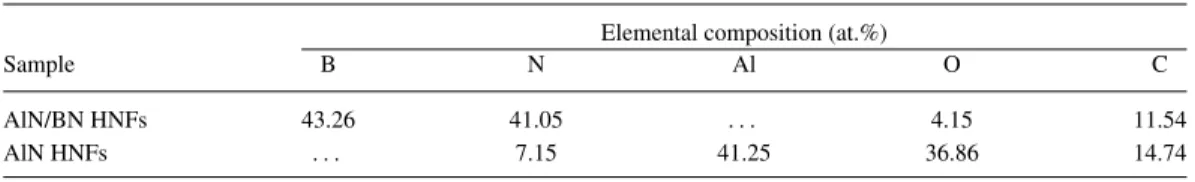
TABLE II. XPS survey scan results of AlN and AlN/BN bishell HNFs.
Elemental composition (at.%)
Sample B N Al O C
AlN/BN HNFs 43.26 41.05 . . . 4.15 11.54
AlN HNFs . . . 7.15 41.25 36.86 14.74
(111), are weakly pronounced. The observed reflections of h-BN in GIXRD pattern are in close agreement with the SAED analysis results.
In order to investigate the chemical composition, bonding states, and impurity content of the films, XPS was conducted on AlN/BN bishell HNFs synthesized using electrospun nylon nanofibers as template. Survey scans from the surface of AlN/BN bishell HNFs indicated the presence of B, C, N, and O, while from the surface of AlN HNFs, it indicated the presence of Al, C, N, and O. It must be noted that the large spot size of X-ray beam (400μm) interacts with a large number of HNFs and collects data from∼5–10 nm range in survey scan. This data probably represents outer surface of HNFs and some part of the inner surface of HNFs which is exposed to X-ray beam through the openings of outer shell layer. TableIIshows elemental atomic percentages obtained from survey scan results of AlN/BN bishell and AlN HNFs. It illustrates that AlN/BN HNFs are nearly stoichiometric with relatively low impurity content. Considerably large amount of O in AlN HNFs is possibly due to oxidation of AlN upon annealing in air ambient. On the other hand, relatively low oxygen content (4.15 at.%) manifested in AlN/BN HNFs might be due to high oxidation resistance of BN.38 Moreover, stainless steel hollow cathode plasma (HCP) source used in this study was found as an alternative to inductively coupled RF-plasma (ICP) source for avoiding the oxygen contamination problem in PA-ALD-grown III-nitride thin films.32Low oxygen content in AlN/BN bishell HNFs can be partly attributed to the superiority of HCP in comparison with ICP. The 11.5% and 14.7% C present in AlN and AlN/BN HNFs, respectively, might correspond to surface contamination and residues left after calcination. The B 1s and N 1s high-resolution XPS scans obtained from AlN/BN bishell HNFs are shown in Figs.4(c)and4(d), respectively. The XPS spectra were analyzed to inspect the possible bonding schemes within the HNFs. Both B 1s and N 1s high-resolution XPS spectra were fitted by merely almost-symmetrical single peaks with binding energies of 190.7 and 398.4 eV, respectively, which confirms not only the presence of BN, but the low-impurity concentration as well.39,40
In this study, we have reported on the template-based fabrication and characterization of AlN/BN bishell HNFs. AlN/BN HNFs were fabricated by depositing AlN on electrospun polymeric nanofi-brous template by HCPA-ALD, which was followed by the removal of polymeric template by calcination and low-temperature sequential plasma-assisted CVD of BN, respectively. SEM and TEM studies have shown a 3D network of AlN/BN nanofibers which imitated the shape and di-mensions of electrospun nanofibers. HCPA-ALD grown AlN layer was conformal and uniform as a result of self-terminating gas-solid reactions occurring at the nanofiber surface, while a branched and rough 3D surface morphology with nanoneedle crystallites has been observed for the CVD grown BN outer layer. Synthesized AlN/BN bishell HNFs were found to be polycrystalline with a hexagonal structure along with low-impurity content. The results of this study show that the com-bination of electrospinning and plasma-assisted low-temperature ALD/CVD can produce highly controlled multi-layered bishell nitride ceramic hollow nanostructures. Electrospinning parameters can be controlled to achieve nanofibrous templates with different average fiber diameters and self-limiting reactions of PA-ALD provide precise control over the wall thicknesses of AlN and BN layers with sub-nanometer accuracy. Such high surface area nanostructured AlN/BN coatings might find potential use in composite reinforcement, chemical sensing, and gas adsorption.
This work was performed at Bilkent University – National Nanotechnology Research Center (UNAM) supported by the Ministry of Development of Turkey through the National Nanotechnology Research Center Project. This work was supported by the Scientific and Technological Research
096109-8 Haideret al. APL Mater. 2, 096109 (2014)
Council of Turkey (TUBITAK) with Grant Numbers 109E044, 112M004, 112E052, 112M482, and 113M815. N.B., A.K.O., and T.U. acknowledge support from FP-7 Marie Curie International Re-integration Grant (Grant Numbers PIRG05-GA-2009-249196 and PIRG04-GA-2008-239444) and NANOWEB (Grant No. PIRG06-GA-2009-256428), respectively. F.K. acknowledges TUBITAK-BIDEB 2232 scholarship. Authors would like to acknowledge M. Guler from UNAM for HR-TEM measurements. A.H. acknowledges Higher Education Commission of Pakistan (HEC) for Human resource development (HRD) fellowship for MS leading to PhD.
1Y. Liu, J. Goebl, and Y. Yin,Chem. Soc. Rev.42, 2473 (2013). 2E. V. Skorb and D. V. Andreeva,Polym. Chem.4, 4834 (2013).
3K. Ariga, Y. Yamauchi, G. Rydzek, Q. Ji, Y. Yonamine, K. C.-W. Wu, and J. P. Hill,Chem. Lett.43, 36 (2014). 4J. Lu, J. W. Elam, and P. C. Stair,Acc. Chem. Res.46, 1806 (2013).
5J. Hamalainen, M. Ritala, and M. Leskela,Chem. Mater.26, 786 (2014). 6R. L. Puurunen,J. Appl. Phys.97, 121301 (2005).
7N. Suzuki, T. Kimurab, and Y. Yamauchi,J. Mater. Chem.20, 5294 (2010). 8Y. Yamauchi, N. Suzukia, and T. Kimurac,Chem. Commun.38, 5689 (2009).
9Z. Zhou, J. J. Zhao, Y. S. Chen, P. V. Schleyer, and Z. F. Chen,Nanotechnology18, 424023 (2007). 10A. Ahmadi, N. L. Hadipour, M. Kamfiroozi, and Z. Bagheri,Sensor. Actuat. B161, 1025 (2012).
11V. N. Tondare, C. Balasubramanian, S. V. Shende, D. S. Joag, V. P. Godbole, S. V. Bhoraskar, and M. Bhadbhade,Appl.
Phys. Lett.80, 4813 (2002).
12Q. Wu, Z. Hu, X. Z. Wang, Y. N. Lu, X. Chen, H. Xu, and Y. Chen,J. Am. Chem. Soc.125, 10176 (2003). 13L. W. Yin, Y. Bando, Y. C. Zhu, D. Golberg, and M. S. Li,Adv. Mater.16, 929 (2004).
14C. Ozgit-Akgun, F. Kayaci, I. Donmez, T. Uyar, and N. Biyikli,J. Am. Ceram. Soc.96, 916 (2013). 15R. T. Paine and C. K. Narula,Chem. Rev.90, 73 (1990).
16B. G. Demczyk, J. Cumings, A. Zettl, and R. O. Ritchie,Appl. Phys. Lett.78, 2772 (2001). 17D. Golberg and Y. Bando,Appl. Phys. Lett.79, 415 (2001).
18X. Blase, A. Rubio, S. G. Louie, and M. L. Cohen,Europhys. Lett.28, 335 (1994).
19J. J. Pouch and S. A. Alterovitz, Synthesis and Properties of Boron Nitride (Trans Tech Publications, Z¨urich, 1990). 20Y. H. Gao, Y. Bando, K. Kurashima, and T. Sato,Scripta. Mater.44, 1941 (2001).
21C. Zhi, Y. Bando, C. Tang, S. Honda, K. Sato, H. Kuwahara, and D. Golberg,Angew. Chem. Int. Edit.44, 7929 (2005). 22R. Ma, Y. Bando, H. Zhu, T. Sato, C. Xu, and D. Wu,J. Am. Chem. Soc.124, 7672 (2002).
23X. Hou, Z. Yu, Y. Li, and K. Chou,Mater. Res. Bull.49, 39 (2014).
24D. Golberg, Y. Bando, P. Dorozhkin, and Z. C. Dong,MRS Bull.29, 38 (2004). 25D. Golberg, Y. Bando, C. C. Tang, and C. Y. Zhi,Adv. Mat.19, 2413 (2007). 26S. M. Nadeem and L. Tong,J. Nanosci. Nanotechnol.14, 1389 (2014).
27J. Kim, D. Shi, K. Kong, Y. Heo, J. H. Kim, M. R. Jo, Y. C. Lee, Y. M. Kang, and S. X. Dou,ACS Appl. Mater. Interfaces
5, 691 (2013).
28G. Jeong, J. Kim, M. Park, M. Seo, S. M. Hwang, Y. Kim, Y. Kim, J. H. Kim, and S. X. Dou,ACS Nano8, 2977 (2014). 29I. Donmez, F. Kayaci, C. Ozgit-Akgun, T. Uyar, and N. Biyikli,J. Alloy Compd.559, 146 (2013).
30X. Fang, S. Li, X. Wang, F. Fang, X. Chu, Z. Wei, J. Li, X. Chen, and F. Wang,Appl. Surf. Sci.263, 14 (2012). 31Q. Peng, X. Sun, J. C. Spagnola, C. Saquing, S. A. Khan, R. J. Spontak, and G. N. Parsons,ACS Nano3, 546 (2009). 32C. Ozgit-Akgun, E. Goldenberg, A. K. Okyay, and N. Biyikli,J. Mater. Chem. C2, 2123 (2014).
33F. Kayaci, C. Ozgit-Akgun, I. Donmez, N. Biyikli, and T. Uyar,Appl. Mater. Interfaces4, 6185 (2012). 34F. Kayaci, C. Ozgit-Akgun, N. Biyikli, and T. Uyar,RSC Adv.3, 6817 (2013).
35A. Haider, C. Ozgit-Akgun, E. Goldenberg, A. K. Okyay, and N. Biyikli, “Low-Temperature Deposition of Hexagonal
Boron Nitride Via Sequential Injection of Triethylboron and N2/H2Plasma,”J. Am. Ceram. Soc.(in press) 36A. Pakdel, Y. Bando, D. Shtansky, and D. Golberg,Surf. Innov.1, 32 (2013).
37See supplementary material athttp://dx.doi.org/10.1063/1.4894782for TEM images of AlN coated nylon nanofibers. 38L. H. Li, J. Cervenka, K. Watanabe, T. Taniguchi, and Y. Chen,ACS Nano8, 1457 (2014).
39M. Das, A. K. Basu, S. Ghatak, and A. G. Joshi,J. Eur. Ceram. Soc.29, 2129 (2009). 40X. Gouin, P. Grange, L. Bois, P. L’Haridon, and Y. Laurent,J. Alloy Compd.224, 22 (1995).