Г к
η
? 1 · Í9
‘ Г 4 ' ? î l ' S ' 3 U i::r л.::;;|.^/„ЛП|Г·;··; ГЯДл r!'^‘''F^;7?VTiríóí Λ Μ
' . ■ ■ іГ ..■. : ·'"■ »?^·· ■* —*,, , . η. I Г| ( ' .-. ’τ ' v ’V’-v/ivjr’ rxj· !χ Λ, I ·"'V i · ' ' ,·’ ‘·».? .. * V ·■ — ' ·■ ■** — •V»·);· T ^ ;: T :* , ’ ■‘ '*'¡, ’^-· V ; - ’ i rFABRICATION, CHARACTERIZATION, AND
PARAMETER EXTRACTION OF GaAs MESFETS
A THESIS
SUBMITTED TO THE DEPARTMENT OF PHYSICS AND THE INSTITUTE OF ENGINEERING AND SCIENCE
OF BILKENT UNIVERSITY
IN PARTIAL FULFILLMENT OF THE REQUIREMENTS FOR THE DEGREE OF
MASTER OF SCIENCE
By
Erhan Polatkan Ata
28 January 1994
•
6 3
I certify that I have read this thesis and that in my opinion it is fully adequate, in scope and in quality, as a dissertation for the degree of Master of Science.
lialtiogl’
Assoc. Prof. Recai Ellialtioglu (Supervisor) I certify that I have read this thesis and that in my opinion it is fully adequate, in scope and in quality, as a dissertation for the degree of Master of Science.
I certify that I have read this thesis and that in my opinion it is fully adequate, in scope and in quality, as a dissertation for the degree of Master of Science.
Assist. Prof. Erkan TekmAn Approved for the Institute of Engineering and Science:
*rof. Mehmet Baray^;
Abstract
FABRICATION, CH ARACTERIZATION , AND PARAM ETER
E X T R A C T IO N OF GaAs MESFETS
Erhcin Polatkan Ata
M. S. in Physics
Supervisor: Assoc. Prof. Recai Ellialtioglu
28 January 1994
Metal Semiconductor Field Effect Transistor (MESFET) is the most widely used active element of today’s microwave industry. After development of the MESFET technology, the microwave industry gained a high acceleration, especially in the telecommunication field.
In this study, GaAs MESFETs with various dimesions and geometries were fabricated. Characterization and parameter extraction of these devices were performed, by means o f low and high frequency measurements. The low cut off frequency of the MESFETs produced were attributed to the non-optimized gate recess etch.
Keywords: MESFET, GaAs, Schottky Contact, Ohmic Contact, active channel, analytical model, small-signal model.
özet
GaAs MESFET ÜRETİMİ, KARAK TER IZASYO N U VE
PARAMETRELERİNİN ELDESİ
Erhan Polatkan Ata
Fizik Yüksek Lisans
Tez Yöneticisi: Doç. Dr. Recai Ellialtioğlu
28 Ocak 1994
Metal Yarıiletken Alan Etkili Transistor (MESFET), günümüz mikro dalga endüstrisinin en yaygın kullanılan elemanıdır. MESFET teknolojisinin gelişmesinden sonra mikrodalga endüstrisi, özellikle iletişim alanında, önemli ivme kazanmıştır.
Bu çalışmada, değişik boyut ve geometrilerde GaAs MESFETler üretilmiştir. Bu cihazların karakterizasyonu ve parametrelerinin eldesi alçak ve yüksek frekans bölgelerinde yapılan ölçümlerle gerçekleştirilmiştir. Üretilen MESFETlerin düşük kesim frekansları, optimize edilmemiş kapı (gate) oyuğu aşındırmasına bağlanmıştır.
Anahtar Sözcükler: MESFET, GaAs, Schottky eklemi, ohmik eklem, aktif tabaka, analitik model, küçük sinyal modeli.
Acknowledgement
I am grateful to Assoc. Prof. Dr. Recai Ellialtioglu for his guidance, motivation, and invaluable supervision during my graduate study.
I wish to express my sincere gratitude to Dr. Nacer Debbar who introduced me to the semiconductor technology.
Special thanks are due to Ahmet Oral, Ismet Kaya, and Erkan Tekman for their invaluable supports, helps, and friendship.
I wish to thank to members of the Advanced Research Laboratories and physics department, without whom this study would be impossible.
I am in debt to family and friends for their supports and patience.
This project was performed under the auspices of the Ministry of Defense, Undersecretariat for Defense Industries, Grant No: SSM-90-AG-033.50.
Contents
Abstract Özet Acknowledgement Contents List of Figures 1 Introduction 1.1 Introduction . . . . 1.2 The MaterialrGaAs 11 IV Vll 1 1 3 1.2.1 Properties of G a A s ... 4 1.2.2 Growth of GaAs ... 82 M E S F E T Principles and Design 13 2.1 GaAs M E S F E T ... 13
2.1.1 Basic Structure and I/V C h a ra cteristics... 13
2.1.2 Output Conductance and Transconductance... 15
2.1.3 Capacitance-Voltage Characteristics... 17
2.1.4 Second Order E ffe c ts ... 18
2.2 Analytical Models for MESFETs ... 20
2.2.1 Introduction... 20
2.2.2 The Long-Channel (Shockley) M o d e l ... 20
2.2.3 Velocity Saturation-The Square Law Model ... 23
2.2.4 Complete Velocity Saturation M o d e l ... 27
2.3 Small-Signal M o d e l ... 28
2.4 Design of M E S F E T s ... 31
3 Fabrication Processes 34 3.1 General Outline of a MESFET P r o c e s s ... 34
3.2 Sample C le a n in g ... 35
3.2.1 Cleaning T e ch n iq u e s... 35
3.3 Photolithography... 36
3.4 Wet Etching and Oxide Removal ... 38
3.5 L ift-o ff... 39
3.6 M eta liza tion s... 40
3.6.1 Ohmic C on tacts... 41 3.6.2 Schottky Contacts ... 42 3.7 Actual P r o c e s s e s ... 43 3.7.1 Mesa Isolation... 43 3.7.2 Ohmic Metalization... 44 3.7.3 A llo y in g ... 45 3.7.4 Gate Metalization... 46 3.7.5 Final Metalization ... 47 3.7.6 Dielectric E ncapsulation... 48 4 Measurement Techniques 50 4.1 Low Frequency M easurements... 50
4.1.1 Transmission Line Model-TLM ... 50
4.1.2 DC Characterization of MESFETs ... 54
4.2 High Frequency C h aracterization ... 65
4.2.1 RF Characterization of M ESFETs... 65
4.2.2 RF Measurements... 72
Bibliography
77
List of Figures
1.1 Performance comparison of T W T , BJT, and M E S F E T ... 2
1.2 The partial band structures of GaAs and Si at 300 K ... 5
1.3 The velocity-field characteristics of GaAs and Si conduction electrons 7 2.1 Cross section of a M E S F E T ... 14
2.2 Plan views of M E S F E T s ... 14
2.3 Ideal MESFET I-V characteristics... 16
2.4 /3 at the onset of the saturation vs. Vp... 25
2.5 MESFET small-signal model... 29
2.6 MESFET small-signal model showing physical origins of elements. 30 3.1 Carrier concentration profile of epi-wafer used for fabrication of MESFETs... 44
4.1 A TLM s tru c tu re ... 50
4.2 Two possible diffusion processes for ohmic metallization... 51
4.3 A TLM equivalent circuit for current flow in a thin-layer semiconductor d e v ic e ... 52
4.4 Ida — Vds characteristics of a 1 fim gate length MESFET... 55
4.5 Ida and gm versus Vga curves for 1 gm gate length MESFET. . . . 56
4.6 Comparison of intrinsic and extrinsic transconductances... 57
4.7 Determination of 7 ? c ... 59
4.8 {Idaf^^ versus Vga curve of F A T F E T ... 61
4.9 Semi-log plot of Ig versus ... 63
4.10 Ro versus X g r a p h ... 65
4.11 MESFET small-signal model without parasitic inductances . . . . 66
Chapter 1
Introduction
1.1
Introduction
In a well known article published in 1952, W. Shockley^ introduced the concept of a Field Effect Transistor (FET), and proposed the term “unipolar” to distinguish it from the bipolar transistor. However, the introduction of the Metal Semiconductor Field Effect Transistor (MESFET), which should not be confused with silicon FETs (MOSFET, J-FET), is as late as, 1966 by C.A. Mead. Even though in the early 1970s, according to the journals dealing with microwave components, the GaAs MESFET “had potential,” but would not easily replace its existing competitors. In the field of MESFET applications, main competitors were:
1. The traveling wave tube (T W T ) for low and medium power amplification; 2. diodes, especially Gunn and IMPATT, used as microwave sources;
3. the silicon bipolar transistor, used as low noise or power amplifier, or as a microwave source for frequencies up to 7 or 8 GHz.
At that time bipolar transistors were making great progress, especially in power amplification area. BJTs with power outputs in the order of a few watts at 2-5 GHz range were promising for the silicon industry. Thus in 1970, MESFET
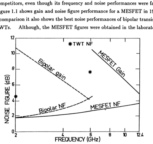
was “unwanted stranger” in the industry, compared with its well-established competitors, even though its frequency and noise performances were far better. Figure 1.1 shows gain and noise figure performance for a MESFET in 1973.^ For a comparison it also shows the best noise performances o f bipolar transistors and TW Ts. Although, the MESFET figures were obtained in the laboratory, they
Chapter 1. Introduction
2
F ig u re 1.1: Performance comparison of TVVT, BJT, and MESFET 1973 state-of-the-art performance comparison between bipolar junction transistor, MESFETs, and traveling wave tubes
clearly show the devices superiority. At the time, very few laboratories attempted to build MESFETs, which were very difficult to produce. The adaptation to the new technology wcis not so simple. First of all the material, GaAs, was quite unfamiliar and difficult to process. The most experienced people in the area were those who were working on Gunn diodes. However the conditions are entirely different: the MESFET has a planar structure; requiring an active layer and an insulating layer, therefore has two interfaces. It also requires a Schottky contact. Second, the factories attempted to start by manufacturing devices with one micron gate length, which was smaller than that normally found
in semiconductor industry at the time.
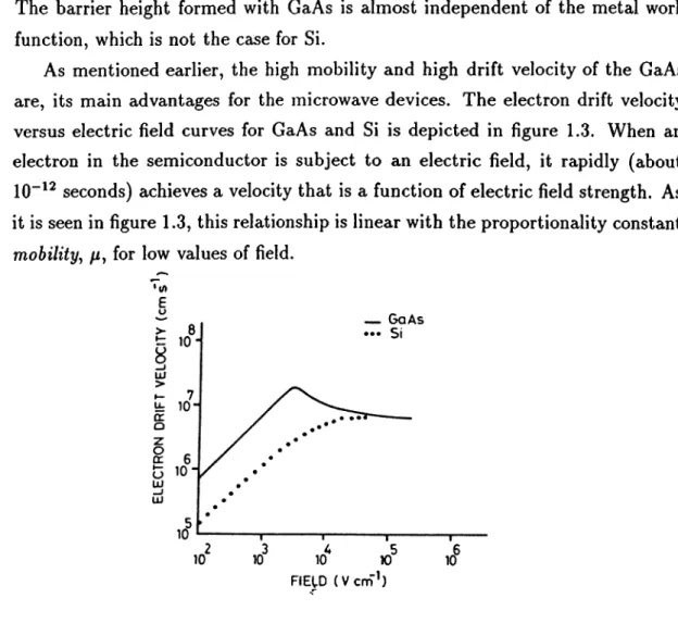
From a few GHz to several tens of GHz frequency range, though leaving its place to High Electron Mobility Transistor (HEMT) and the Heterojunction Bipolar Transistor (HBT), MESFET is the most widely used active component. The success of MESFET is due to the semiconductor material, namely GaAs. Electron mobility in this material, for example 8500 cm?¡V ■ sec versus 1500 for n-type silicon, for the same concentration of carrier densities. Additionally, the maximum saturation velocity for GaAs ( ~ 10^cm/sec) occurs at a lower threshold field (3500 V/cm versus 10000 for Si). Also, GaAs has a better insulating substrate than silicon, which allows low parasitics and true monolithic circuit realization. Finally, GaAs is more radiation tolerant than silicon, which enables its use in space with very low protection against radiation.
Although all of these advantages were known, GaAs was primarily used only in the production of bulk effect diodes, utilizing other specific electrical properties (e.g. electrons moving from one valley to another).
However, even today further efforts are necessary to improve reliability. Optimization of the processes, for efficient and competitive production, is still a major problem. Considerable work has been carried out in these directions, but there are still problems to be solved, such as passivation, reliable ohmic contacts etc., at least by some manufacturers. Short and medium term drifts still cause degradation of devices, and differences in behavior and/or performance can still arise between transistors from different batches.
1.2
The Material:GaAs
Chapter 1. Introduction
3
Over thirty years, GaAs has been the subject of intensive scientific study and a very large literature on the subject formed. There are several reasons for such intensive interest.^
First, GaAs is a compound semiconductor combining group III and group V elements from the same row in the periodic table as the group IV semiconductor, germanium. The charge exchange existent in the bonding of the lattice adds an
ionic component to the mainly covalent bond of Ge and the band gap is expected to increase. This increase in band gap offers a wider range of electrical resistivity and the protection of extrinsic semiconductor behavior to high temperatures as well as some other useful properties. These properties are very valuable for the device physicist and engineer.
Second, as substitutional impurity atoms from groups II, IV, and VI will act as donors and acceptors in the GaAs lattice, extra degrees of freedom are available when compared to Ge or Si.
Third, when the whole family of III-V is investigated, from InSb to AlP including inter-periodic compounds such as InP, AlSb, and alloys such as GaAsP (the first commercially significant III-V semiconductor) or GaAlAs (which allows the band gap to be varied without significantly changing the inter-atomic distance), the potential advantages over the group IV elements Sn, Ge, Si, C (diamond) are even more obvious. The study of GaAs as a prototype is clearly justified in both academic and applied sense.
Chapter 1. Introduction
4
1 .2 .1
P roperties o f G a A s
Cr y s t a l St r u c t u r e
GaAs at room temperature has a density of 5.317^ · cm~^ and crystallizes into zinc blende structure, which consists of two equivalent, inter penetrating face- centered cubic lattices, one containing Ga atoms and the other As atoms. The lattice is broadly equivalent to that of Si, which has a diamond structure, but due to presence of dissimilar atoms, there exist some significant differences in the crystal properties. A shift of valance charge from gallium to arsenic atoms results in a mixed (ionic/covalent) bond compared to the covalent bond in germanium and silicon. This has very significant effects on the electronic band structure and increases the bond strength (the melting point of GaAs is higher than that of Ge).
Another result of the existence of dissimilar atoms is the difference in the chemical activities of opposite (111) crystal faces in GaAs. If (111) planes of
GaAs crystal are considered, it can be seen that all Ga atoms lie on a plane parallel to As atoms, which also lie on another plane 0.8
A
apart, whereas the next nearest Ga plane is 2.4A
apart from As plane. This structure results in observations of different etch rates, depending on the plane (Ga or As) on surface, reacting with etchant. The etch rate difference for different planes causes different etch profiles in different directions, which sometimes may cause problems related to process of GaAs.Chapter 1. Introduction
5
El e c t r i c a l Pr o p e r t ie s o f GaAs
B a n d S tru ctu re In the sense of device physics, the electronic band structure of a semiconductor is its most significant property. The band structure determines the main electrical and optical properties that generate the device functions. Since experimental data give accurate but limited information at particular points in Brillouin zone , a complete and accurate band structure information is difficult to obtain. Theoretical calculations, due to some approximations, can predict the band gap structure only with some uncertainty. However, there exist “working” band structure models. In 1.2 partial band structures of GaAs and Si at 300 K, obtained by the pseudo potential calculations, are seen.^
F igu re 1.2: The partial band structures of GaAs and Si at 300 K
Showing the uppermost valance bands and the lower conduction bands along two of principal directions in the crystals. The magnified (x5) insert shows the detail at Г of the light and heavy hole bands in GaAs (V/ and Vh)
In GaAs and Si, the valance band maxima occur at zero wave vector point (Г) and the nature of the bands at this point determines hole conduction properties. The minimum allowed energy for conduction band states also occur at Г in GaAs but is located near the X point in Si, so the electron wave vector has a finite magnitude and direction [100] for conduction electrons in Si, which affects some electrical and optical properties.
The band gap of GaAs (1.412 eV at 300 K) is larger than that of Si (1.08 eV at 300 K), which in turn results in a lower steady state density of thermally generated carriers in GaAs (10®cm^) compared to Si (10*°cm^). Thus GaAs has the advantage for better isolation (higher resistivity) than Si, which is an important property for lowering device parasitics.
Since the curvature of conduction band minimum of GaAs is higher than that of Si at the conduction band minimum, the electron effective mass in GaAs (О.ОбЗшо at Г) is much lower than that of Si (О.Зшо near X), which, in conjunction with the fact that scattering rates are of similar magnitude, explains the higher mobility of electrons in GaAs. Higher mobility means higher operating frequency, and faster devices.
Chapter 1. Introduction
6
S em i-In su latin g G aA s In practice isolation regions in GaAs is achieved either by mesa etching or by means of forming deep electronic states near the center of the band gap, which lock the position of the Fermi level close to its intrinsic position. Defects can produce electronic states at any position in the band structure and many produce states near the middle of the band gap (deep states). If these deep states are dense enough, they can effectively control the electron occupancy of the crystal, resulting in the pinning of the Fermi level close to the defect state energy. For example, substitutional chromium atoms on the gallium sites, produce deep state close to the center of the gap and are used to control the resistivity. Lattice damage caused by irradiation with fast particles (electrons, protons, ions) also produces deep states, whereas proton is the preferred one due to its better depth and spreading characteristics.^
whose active layer thicknesses are very small, the surface phenomena can be critical for some applications. The termination of the crystal at the crystal surface causes some electronic state formation. When a metal comes in intimate contact with semiconductor, depletion barriers can be generated (this is the case for GaAs). If this barrier height is very small or if some extra work is done to obtain a locally high carrier concentration in the semiconductor to form a thin barrier allowing high electron tunneling rate, ohmic contacts are formed. If these conditions are not satisfied the barrier results in a rectifying Schottky contact. The barrier height formed with GaAs is almost independent of the metal work function, which is not the case for Si.
As mentioned earlier, the high mobility and high drift velocity of the GaAs are, its main advantages for the microwave devices. The electron drift velocity versus electric field curves for GaAs and Si is depicted in figure 1.3. When an electron in the semiconductor is subject to an electric field, it rapidly (about 10"^^ seconds) achieves a velocity that is a function o f electric field strength. As it is seen in figure 1.3, this relationship is linear with the proportionality constant
mobility, fi, for low values of field.
Chapter 1. Introduction 7
Figure 1.3: The velocity-field characteristics of GaAs and Si conduction
1 .2 .2
G row th o f G a A s
The MESFET requires bulk material for substrates and epitaxial material for the high quality active region. Both must be doped to the correct carrier type and impurity level. The management of these processes is extremely critical because it is the most important determining factor in the final device performance, especially for the microwave devices where the operation depends so much in purity and characteristic of the epitaxial material.
The substrate is necessary as a mechanical support for the very thin epitaxial layer, and acts as a basement during growth of epitaxial layer. Commercially available substrates’ thicknesses vary in the 100-500 pm range. For planar devices, such as MESFETs and logic elements, substrate resistivities must be in the 10“* — 10®ilcm range.
Chapter 1. Introduction
8
Bu l k Gr o w t h
Bulk material is usually grown in the form of large ingots of single crystal; the major problem to be overcome during growth of the compound semiconductor arises due to the high vapor pressures resulting at growth temperature. These volatile components must be contained either by growth in a completely sealed system or by suppression of the volatilization by encapsulation of the melt in an inert liquid
Bulk ingots are usually produced using the Liquid-Encapsulated Czochralski
(LEG) technique,® in which the crystal is slowly rotated and pulled out from a melt through a molten boric oxide encapsulant, at the melting temperature of GaAs (1513 K). While this is a lower temperature than that of Si, the equilibrium overpressure and stoichiometry control problems are the drawbacks compared to Si.
Another method, widely used for production of large quantities of em n- GaAs substrate material is the Horizontal Bridgeman (HB) technique.® The main advantage of this method is that, it is readily automated. A boat containing the semiconductor compound and crystal seed is sealed inside a quartz tube, the
other end of which contains a small arsenic excess. The furnace consists of at least two zones, one held at 612°(7 in which the arsenic end of the tube sits. The ingot is melted at 1270°(7 and moved slowly out of the hot area into the cooler one, resulting in a crystallization. The completed crystal usually has a shape defined by the shape of the boat, somewhat circular up to the level of the melt. This “ D” shaped crystal is sawn perpendicular to (100) axis and made round.
Even though, by using variations of above two methods, the grown GaAs crystal has many dislocations. These dislocations not only introduce trapping states, alter the etching properties of the wafer, but most importantly can affect the electrical performance of the devices. Exactly how this occurs is not known, up to our knowledge, but it is proposed that dislocations affect the activation energy of ion-implants. Studies have shown that source-drain current and threshold voltage of logic FETs are strongly correlated with dislocation density.® In general LEG material exhibits a greater dislocation density than that of HB material. This is mainly due to the higher temperature gradient in the LEG method. The problems due to these dislocations can be solved by epitaxial growth of a GaAs buffer layer which will be virtually dislocation free and will heal dislocation propagation to the active part of the material.
After a useful substrate is obtained by growth and processes such as sawing, grinding, polishing, etc., an active region for devices must be formed on the substrate. This is done either by epitaxial growth or ion implantation.
Chapter 1. Introduction
9
Ep i t a x i a l Gr o w t h
Material of highest electrical quality is produced by epitaxial growth, i.e.
production of controlled thin film, techniques at temperatures between 900 and 1100 K. The growth of such layers are essential to all state of the art devices. The active region of the component can be defined in thickness, carrier type, and impurity level and profile to optimize performance. The low growth temperatures enable both impurity and stoichiometric defects to be controlled at concentrations below lO’ ^cm“ ^, which cannot be obtained in ingots. Epitaxial layers are generally of higher crystal quality than the substrate they are grown.
Chapter 1. Introduction
10
Although crystal defects tend to propagate in the immediate epitaxial layers, as the layers gets thicker some healing takes place. If an active (doped) layer is directly grown on the substrate, the impurities and defects in the substrate will degrade the crystalline properties and therefore the electrical properties of the material. Thus, buffer layers of un-doped GaAs are usually epitaxially grown on the substrate before active layers are grown.
There are, basically, three types of epitaxy used for GaAs, namely Liquid Phase Epitaxy (LPE), Vapor Phase Epitaxy (VPE), and Molecular Beam Epitaxy
(M BE).
LPE is the oldest technique used to grow epitaxial layers on GaAs crystals. It is an inexpensive method and is capable of growing many material compositions including GaAlAs, but unfortunately not suitable for microwave devices. In this technique, a GaAs substrate is placed on a slider that can be moved across surfaces of molten materials contained in boats. These melts are gallium saturated with the desired materials, such as As (to form un-doped GaAs) or dopants. The temperature gradients are such that the melts are just at the solidification temperatures, so that they solidify onto the crystal substrate. The major problem of LPE is the difficulty of growing uniform layers over large surface areas. However, this technique gives successful results for LEDs and such structures, which, in contrast to microwave devices, do not need thin, uniform high quality epitaxial layers.
VPE is one of the most frequently used methods for epitaxial growth. In this method, the Ga, As, and the dopant atoms are brought to the wafer in gaseous phase. Under appropriate physical conditions, reactions take place on the surface of substrate that result in deposition of the atoms on the surface such that they replicate the crystal structure. There are mainly two variations of VPE. In the VPE technique with trichloride transport, the substrate is placed in a quartz slice holder in a reactor tube. At a temperature close to 800 °C, growth is obtained by the reaction of AsCU with Ga in the presence of H2 to produce
GaCl, As4 and HCl. Although wide usage of this method, its limitations in terms
Chapter 1. Introduction
11
VPE system using an organometallic compound for gallium transport, namely
Metal-Organic Chemical Vapor Deposition (MOCVD). In this method, generally trimethylgallium (Ga(CH3)3) is used as the Ga source and arsine (ASH3) is used as
the arsenic source. The main advantage of the method are the ability to produce complex heterostructures and the good control of both layer thickness and doping. Major problems of this system is its high cost and safety requirements related to arsine.
MBE is another major method of growing epitaxial layers. In this technique substrate is placed in an ultra high vacuum (generally 1 0“ ^° to 1 0“ " torr)
and required materials are evaporated from ovens (effusion cells) and stick on the heated substrate to form an epitaxial layer. With proper control of the sources (Ga, As, Al, Si, etc.) almost any material composition and doping can be obtained. Even single atomic layer growth is possible. MBE’s advantages are that it can produce almost any epitaxial layer composition, layer thickness, and doping, and can do so with high accuracy and uniformity across a wafer. Disadvantages include high vacuum requirements, complex and costly equipment, and slow growth rate. Ultra high vacuum, that is required in the growth chamber, is extremely difficult to maintain, especially in the presence of heated substrates and heated effusion cells. Growth rate is typically a few microns per hour, which is very low compared to other techniques which have approximately a few microns per minute growth rates.
Io n Im p l a n t a t i o n
Ion implantation remains as the most economical method to form active layers for GaAs MESFET devices. In this procedure, dopant atoms are introduced into the substrate surface by ion implantation, with typical energies and doses of 30 keV to 400 keV and 10^^ to VV* atoms ¡cm?. Such implantation greatly damages the crystal lattice. This damage is healed by the method known as ’’ activation of implant” , in which a high temperature annealing step (~850 °C) is performed to anneal out the lattice damage and allow the implanted atoms to move onto lattice sites. Activation is generally in the order of 75% to 95%, and depends on the
Chapter 1. Introduction
12
implanting and annealing conditions. Main advantages of implantation are , its well establishment due to silicon industry, high uniformity over a wafer, economy, and capacity. Beyond these there is another major advantage, doping can be performed locally by selectively masking the wafer, no other technology offers such a flexibility (at least without major complications). The main disadvantage of the ion implantation is that the doping profile transition cannot be as abrupt as the epitaxial methods, since the implanted donors nearly follow a Gaussian distribution.
Chapter 2
M ESFET Principles and Design
2.1
GaAs MESFET
2.1.1
Basic Structure and I / V Characteristics
MESFET in its geometrical structure, is very similar to Field Effect Transistor
(FET) introduced by W. Shockley in the early 1950s.^ Cross section and planar views of general structure of a MESFET is depicted in figures 2.1 and 2.2. Three metal electrodes, namely gate, drain, and source are in contact with a thin semiconductor (n-GaAs in this work) active layer. Contacts to both source and drain are accomplished by means of ohmic metallization, whereas, the gate is a Schottky barrier contact. Current through the active layer, the channel, can be controlled by the depletion region formed by the Schottky gate. As the reverse bias on the gate increases, the depletion layer penetrates deeper into the active region, and vice versa. When there is no potential difference between source and drain, the depletion region is symmetrical, however in normal operating conditions, drain is biased to a higher potential than source, thus gate-drain junction is more reverse biased than gate-source junction resulting in a deeper
depletion region on the drain side.
Most microwave MESFETs, and those produced in our laboratory, are depletion mode devices. In this kind of devices, when there is no bias applied on
Chapter 2. MESFET Principles and Design 14 -/ y f /y
h
1
y / V / / 7 7 ' SOURCE / < / y y y y / y y y y y / / ' ^ O R A I N / / *ch + ■!■ + ---d(x) k : — — I ^ A ^ ch sub sub SUBSTRATEF igure 2.1: Cross section of a MESFET
F igure 2.2: Plan views of MESFETs (a) MESFET with “T” type gate, (b) MESFET with “II” type gate
the gate, the depletion layer does not penetrate all through the active region, thus there exists a low resistance path for current through the drain-source terminals, namely the drain-source current, Ijs- Enhancement mode devices do not conduct current through drain-source contacts, unless a forward gate bias is applied. In this work enhancement MESFETs are disregarded. Hereafter, the term MESFET stands for n-GaAs depletion type device. For a depletion type MESFET, when
Chapter 2. MESFET Principles and Design
15
enough reverse bias is applied, the depletion region will extend across the entire active channel and will result in, although not infinity due to leakage currents, a high drain to source resistance. The potential required to deplete the channel is the “threshold voltage” , Vr·, and the corresponding phenomenon is known as “pinch-ofP condition. For reasonably low biases, the current through the source-drain contacts is linearly proportional to the applied bias. Thus for small biases the region in between the source-drain terminals behave like an almost linear resistor. For larger biases, however, the semiconductor material (GaAs) itself limits the maximum carrier velocity, causing current saturation to occur. Figure 2.3 shows the current-voltage relationship expected from an ideal MESFET, as just described.
Actual MESFET I-V characteristics are similar to the ideal characteristics, with the important exception that the slope of the curves remains slightly positive even after saturation velocity is reached, which is due to the finite output conductance of the device. Charge domain formation, charge injection into the non-ideal semi-insulating substrate, surface effects and channel-substrate interface states are the main reasons of the finite conductivity. The magnitude of the current for a given drain-source bias will be directly proportional to the gate width, Z, of the device. On the other hand gate length, L, mainly determines device’s gain and frequency characteristics. Gain and cut-off frequency, / j , increases with decreasing gate length.
It is important to note that, for an optimal device performance, a decrease in gate length must be compensated with corresponding decrease in other device dimensions as well as an increase in channel doping densities.
2 .1 .2
O utput C on ductan ce and Transconductance
For analog applications, the I-V curves are not as useful as their derivatives. The derivative of drain-source current with respect to drain-source voltage, while gate-source voltage is kept constant, is defined as the output conductance of the MESFET, gds,
Chapter 2. MESFET Principles and Design
16
DRAIN-SOURCE VOLTAGE
F igu re 2.3: Ideal MESFET I-V characteristics.
Ideal drain-source current as a function of drain-source voltages for several gate-source voltages.
9ds —
rds
' did A
dVds), (2.1)
where rds is output resistance sometimes used instead of output conductance. The output conductance of the device is an important characteristic in analog applications, due to the fact that it plays a significant role in determining the maximum voltage gain available from the device and optimum output matching properties. Generally low output conductance, equivalently high output resistance, is required, which means flat Ids — Vds curves. Output conductance is directly proportional to device gate width and inversely proportional to channel doping concentration, Nd·, and active layer thickness , a.
Since deep levels play an important role in determining the output resistance of GaAs MESFETs, these characteristics are strongly frequency dependent at relatively low frequencies (DC to approximately 1 MHz).
Chapter 2. MESFET Principles and Design 17
The device transconductance, ÿm, is defined as the slope of the /¿j — Vgs
characteristics with the drain-source bias kept constant,
9m — 'did,
dV,
(
2.
2)
/ V.,,
The transconductance of the MESFET is one of its most important indicator of device quality for microwave and millimeter wave applications. When all other characteristics are equal, a device with high transconductance will provide higher gains and better high frequency performance. Transconductance of MESFET is directly proportional to gate width and is inversely proportional to gate length. Deep levels cause a decrease in the transconductance, by the increasing frequency. Measured microwave transconductances are typically mentioned to be 5 to 25 % lower than measured DC values.
2 .1 .3
C ap acitan ce-V oltage Characteristics
Gate-source capacitance of a MESFET is defined as. _ f dQg
9^/ V
9<i (2.3)where Qg is the depletion region charge beneath the gate, similarly gate-drain capacitance can be defined as.
(2.4)
Since source terminal is grounded under typical operating conditions, gate- source and drain-source bias voltages are those directly controlled. Thus, gate- source capacitance is often defined g.s.
Chapter 2. MESFET Principles and Design
18
dQg
dVa9»/ Kd. (2.5)
Equations 2.3 and 2.5 are not equivalent, but describe slightly different
quantities. This difference is usually small but can be significant if calculations are based on physically based models. Nevertheless, these capacitance definitions are not used in theoretical or experimental studies, instead, use of equivalent circuit capacitances is preferred.
The gate-source capacitance is one of the main parameters that determine the input impedance and frequency performance. To first order, the input impedance of a MESFET in a standard common source configuration, with typical bias levels applied, is simply the impedance of the gate-source capacitance in series with a few ohms of resistance. Thus, gate-source capacitance must be reduced to improve the high frequency performance. The gate-source capacitance increases with increasing gate length, gate width, channel doping density, and gate-source voltage. The dependence on geometry is not linear due to fringing charge effects.
It is clear that the gate-drain capacitance of MESFET is closely related to gate-source capacitance. In the normal mode of operation for amplifiers and oscillators, primary characteristic affected by the gate-drain capacitance is the reverse isolation of the device. Gate-drain capacitance increases with increasing gate length, gate width, channel doping density, and gate-drain voltage, similar to gate-source capacitance as expected because of symmetry.
2 .1 .4
Second O rder Effects
The basic operating principles discussed up to this point do not explain some deviations from ideal characteristics under certain operating conditions. However, for some applications an understanding of such deviations from first order theory can be critical. Especially, the low frequency dispersion of device characteristics, and the behavior of the device near pinch-off often cause deviations from the first order predictions. Device characteristics which have been observed to
Chapter 2. MESFET Principles and Design
19
shift at low frequencies include output resistance, transconductance, and device capacitances.® For small signal applications these effects can be ignored since the frequency of interest is well above these frequencies, but for large signal applications these effects must also be taken into account.
Ou t p u t Re s is t a n c e a s a Fu n c t io n o f Fr e q u e n c y
Many of the electrical characteristics of GaAs MESFETs shift dramatically at low frequencies® (below about 1 MHz). As frequency is increased above DC, device output resistance can drop by as much as an order of magnitude. The frequency range of the transition can vary from below 10 Hz to more than 1 MHz. Although these frequency dispersion effects take place well below the frequency bands of typical operating frequencies, they still affect the large signal performance. The low frequency dispersion effects also causes complications in the parameter extraction techniques.
Tr a n s c o n d u c t a n c e a s a Fu n c t io n o f Fr e q u e n c y
Low frequency shifts in transconductance values are also observed for MESFETs, whereas the shifts are typically, on the order of 5 to 25 % as mentioned earlier. However, even these small drops in the transconductance can cause unpredictable errors in device modeling applications, especially for large-signal circuitry.
Su b-t h r e s h o l d Ef f e c t s
When MESFET is biased near pinch-off, the physical phenomena that dominate the device performance are different than those under normal operating conditions. As a result the pinch-off occurs more gradually than predicted by most models, which can be extremely important for digital applications and for certain mixer topologies. In the theoretical definition of threshold it is assumed that depletion region is completely free of mobile carriers and the substrate is a perfect insulator. In an actual device, the boundary between the edge of the depletion region and the un-depleted channel is gradual and occurs over
Chapter 2. MESFET Principles and Design
20
a distance of several Debye lengths. A graded transition also occurs between the active channel and the substrate, and as the device is pinched-off, these two graded regions are forced closer to each other. When these two transition regions meet each other the free carrier density in the channel never reaches the background donor density level, also high electric field values at the channel- substrate interface can cause carrier injection into the substrate. These effects cause a more gradual decrease of current as the device is biased towards pinch-off.
2.2
Analytical Models for MESFETs
2 .2 .1
Introduction
Although basic concepts of MESFETs are well understood, device modeling is still a challenging problem. The modeling is important for computer aided design and simulation of circuits. There are several approaches for analytical modeling of low frequency characteristics of MESFETs. In following sections two main approaches, namely “square law” and “complete velocity saturation” models, preceded by an outline of “long-channel” model, are discussed. Square law model provides an accurate model for low voltage pinch-off MESFETs and an approximate description for higher pinch-off voltage MESFETs. The complete velocity saturation model accurately describes high pinch-off voltage devices but overestimates the drain-source current in low pinch-off voltage devices. However, both models take into account the source and drain series resistances and the output conductance, providing simple analytical expressions for current voltage characteristics, which are in good agreement with experimental data.
2 .2 .2
T h e Long-C hannel (Shockley) M o d e l
The analysis of MESFET is usually carried out in parallel to that of JFETs, since their structures are very similar. The first analysis was carried out by Shockley,' with the assumption of two gates, on the two opposite sides of active channel, depleting through the channel. The analysis of MESFET is similar but carried
Chapter 2. MESFET Principles and Design
21
out with a single Schottky gate. In this model a uniform effective channel donor density equal to electron density in the un-depleted active region and a constant mobility is assumed. Thus threshold voltage, Vr is given by
Vt = -Vp
+
Vki(
2.
6)
where, Vp is the pinch-off voltage, defined across the channel and given byqNda^
2ts (2.7)
Shockley also used an approximation so called “gradual channel” , which is based on the assumption that the bias of the gate junction is a slowly varying function of position.
The fundamental equation of the field effect transistor is obtained by integrating incremental potential change from the source side to the drain side of the gate with respect to distance along channel, that is
Eh — 9o \ 1
Vp^
(
2.
8)
where Eh is the channel current, Vi is the voltage drop in the channel across the region under the gate, and
go =
qpNdZa
(2.9) is the conductance of the metallurgical channel. If series resistances of drain to gate and gate to source regions are neglected, then Vi = Vds- Fundamental FET equation is only applicable up to the pinch-off. When W{L) — a (pinch-off condition) current saturation occurs, and the Shockley saturation voltage is
= K. - H.· + Fa
where S stands for Shockley. Thus, the saturation current is
(2.10)
^ch,sat 5*0
I
« T oU , , 2 ( H . - Fg)3
Chapter 2. MES F E T Principles and Design
22
The transconductance in the linear region can be derived from fundamental equation as
9 m — 90~
VK + Hi - Vo - VH, - Vb
(2
.12
)and the transconductance in the saturation region is
(2.13) For small drain-source voltages, K <C Vti — Va-, channel current and transconductance can be approximated by
/ ^ I K
-gm - 90
Vp
Vi
2 y/V ,iV u -V a)'
Gate-source and gate-drain capacitances are defined as
dQ
d V I V , — Vq ^-constant r - ^ 1
^ gd — \VQ=constant
Q is the total charge in the depletion region given by
(2.14)
(2.15)
(2.16)
(2.17)
Q = qNiZ ! W (x )d x (2.18) Except in the region close to the pinch-off, where the Shockley model is not applicable because the extension of depleted region beyond the gate should be taken into account, solutions for capacitances can be approximated by^°
C,s = C,d =
a
^50 \/l -____^9 sO____ \/i - Vi,¡Vu (2.19)(
2.
20)
Chapter 2. MESFET Principles and Design
23
where CgsQ CdoO dgO ZL CsqNd(
2.21)
2
V
2
Hi
When there is no bias applied to the MESFET, total gate capacitance is equal to that of the depletion region due to built in potential, which is equally divided between source and drain because of symmetry. For non zero biases, Cgs and Cdg
behave as capacitances of equivalent Schottky diodes connected between the gate and the source, and gate and the drain, respectively.
2 .2 .3
V elocity S atu ration -T h e Square Law M o d e l
Shockley’s model assumes a non saturating electron velocity, which is a very crude approximation. Pucel et proposed a simple approximation for the field dependence of the electron velocity a.ssuming that the velocity is proportional to the electric field until the value of saturation velocity Vg is reached at S — Eg and then becomes constant
V —
(
2.
22)
/x5, S < Eg Vs, P > Ps
The velocity saturation is first reached at the drain side of the gate where the electric field is highest according to the Shockley model, i.e. when E(L) = Eg
which is equivalent to
- = « (2.23)
where
EgL
’ (2.24)
u = V{x)lVp and X = x /L , and origin of x is defined to be on of the gate. For large a, a ^ 1, solution approaches
the source side end
Chapter 2. MESFET Principles and Design
24
which is identical to corresponding equation 2.10 of Shockley model. The opposite limiting case, o; <C 1 and a 2(1 — ■, corresponds to the velocity saturation model
The saturation current is given by
(2.26)
Idss = qNdVsZ{a — W {L)) (2.27) where the depletion region width W {L) at the drain side of the gate is given by
W {L) = a. IVii - Vb +
K, (2.28)
In dimensionless units ( = Idss/goVp) is
is = a ( l - + ug) (2.29) where Us = and uq = dimensionless saturation and gate voltages. In the limiting case, or —> oo (long gate device with a small pinch-oif voltage) equation 2.29 reduces to the corresponding equation 2.10 of the Shockley model. In the opposite case, o; -C 1, (short gate and/or large pinch-off voltage)
is = Oi{l — y/ua) (2.30) which corresponds to the simple analytical model proposed by Shur,^^ and can be approximated by the interpolation formula.
which coincides with the equation used for JFET saturation current in the SPICE modeP^
Idss = 0 i V G -V r y (2.32) where
Chapter 2. MESFET Principles and Design 25
Vt = H,· - K
and transconductance parameter ¡3 chosen as 2CÿpVs Z
(2.33)
(2.34)
a{pVp + SvsL)
This may be an explanation for success of SPICE JFET model used in some cases for MESFETs. The transconductance at the onset of saturation is
9m = 2/3{Vg - Vt) (2.35) Equation 2.34 is dependent on Vp which is a function of two main parameters doping concentration and channel thickness. In figure 2.4, the variation of j3 vs.
Vp characteristics with varying doping and active channel thickness is shown.
F igure 2.4: ¡3 at the onset of the saturation vs. Vp.
(a) Vp varies due to the variation in doping (a=0.1 /xm); (b) Vp varies due to the variation in the thickness of the active layer (Nd = 1.2 x lO^^cm“ ^). Numbers near the curves correspond to the gate lengths in micrometers.
Transconductance at low pinch-ofF voltages increases for devices with sub-micron gates. The values of jd (hence, transconductance for the same voltage swing) increase with the decrease of the device thickness and with the increase in doping. However increase in /? is followed by increase in device capacitances, Cga and
Cdg (see equations 2.19- 2.21), while the parasitic capacitances do not increcise, therefore thin and highly doped layers increase the operation speed. High doping
Chapter 2. MESFET Principles and Design
26
also has the advantage of decreased active layer thickness for a given value of the pinch-off voltage, which makes it possible to minimize short channel effects which are observed for Lja < 3.^“*
The analyses given above are valid only for the case when electron velocity saturates at the drain side of the gate. At higher drain-to-source voltages the electric field in the channel increases, resulting in velocity saturation in larger portion of the channel (gate length modulation). This effect was noted by Pucel, Haus, and Statz,^^ so that the models that include gate length modulation are sometimes referred to as the PHS (Pucel-Haus-Statz) model, although two region model is a more commonly used name. Works of Shockley^ and Shur^® results in a rather complicated expression for the saturated portion of gate length, T*. Further work of Curtice^® and Chen et al}^ resulted in the rather simple equation for drain-source current.
Id s — I sat (l-t-AV;)tanh(7?V5) (2.36)
where i]is chosen in such a way that for Vds 0 equation 2.34 transforms into a corresponding equation of the Shockley model.
Tj — Gchfisat (2.37)
where
Gch = go{i· - Vug) (2.38) is the channel conductance at low drain-source voltages predicted by the Shockley model.
go = qNdpZalL (2.39)
is the full channel conductance. This model is referred to as square law model. ExperimentaP® and theoreticaP^ works increase the evidence that square law model is approximately valid for low pinch-off voltage devices. The source and
Chapter 2. MESFET Principles and Design
27
drain series resistances Rs and Rd can be included in the model as follows. The gate voltage is
Vgs = Vg + IsatRs- (2.40) Constant A in equation 2.36 is empirically determined and accounts for the additional output conductance beyond the output conductance due to gate length modulation. The drain-source voltage is
^ D S — K ’ + h a t { R s + R d ) (2.41) which completes the set of equations of analytical square law model. Last thing to note is that, this model has the slight difference from Curtice model,*® used for parameter extraction in our laboratory, that it includes the gate length modulation effect and source and drain series resistances.
2 .2 .4
C om p lete V elocity Saturation M od el
The value of ^ approaches to the value which corresponds to complete velocity saturation everywhere in the channel when
K, > 35,L. (2.42)
For Ipm gate MESFETs EsL is close to 0.3-0.4 V so that above condition is satisfied by pinch-off voltages higher than 3 V. At such pinch-off voltages the assumption of complete velocity saturation in the channel becomes v a lid ,w h ic h means that at large drain-source voltages, voltage drop, Vgi, across the region where electron velocity is not saturated, can be neglected compared with Vt, — Vg
V,.· < H. - Vg.
The expression for drain-source saturation current for this case is*^
(2.43)
Chapter 2. MESFET Principles and Design 28
According to equation 2.42 this equation may not be satisfactory close to the threshold when voltage drop 14,· may lead to a considerable relative change in the width of the un-depleted region and hence in the drain-source saturation current. However, even in this region equation 2.44 can still be used as a satisfying interpolation formula.
The source series resistance does not change Vgs (compared to Vq) at low values of Vi because the values of the channel current and hence of the voltage drop across are small, which enables the use of the same interpolation formula (equation 2.36) for drain-source current as for the square law model.
Ids — ^5ai(l T A Vi) tanh(i/Vi) (2.45)
where tj is chosen in such a way that, as Vus 0 above equation transforms into a corresponding equation of the Shockley model
V = Gch
^sat (2.46)
where Gch is given by equation 2.38, constant A is the same empirical constant which is used in the square law model to account for the output conductance. The drain-source voltage
Vds = K· + IsatiRs + Rd) (2.47)
completes the set of equations for analytical complete velocity saturation model.
2.3
Small-Signal Model
Small-signal MESFET model is very important for a circuit designer since it provides lumped element approximation for the device, which can be used in circuit simulators. A well chosen model, with properly extracted elements will work for frequencies higher than those at which model parameters are extracted. Another property of this model is that it enables device scaling, which enables performance prediction of unmeasured devices which can be scaled to a modeled
Chapter 2. MESFET Principles and Design
29
one. In this work the most widely used small-signal model in figure 2.5 is considered. This model has the advantage that its elements can be uniquely determined from parameter data and provides an excellent match with
S-*■0 ^0 ’ 0d + V —
c
gs g Ve y / m ■jurt < V 'v ■'dsF igure 2.5: MESFET small-signal model.
parameters up to 26 GKz7
Eq u i v a l e n t Cir c u it El e m e n t s
In figure 2.6 the small-signal model is drawn on cross section of MESFET, in order to clarify physical origins of model elements. Each of these elements are explained below. The elements other than parasitic ones, namely Lg, Ld, Ls, Rg, Rd, and i?,, make the intrinsic MESFET.
P a ra sitic In d u ctan ces The parasitic inductances are mainly due to the metal pads of the device, therefore they are highly geometry dependent and analytical modeling is extremely hard. In general, gate inductance is higher than drain and source ones, especially for short gate length devices. Typical values given in literature^ are on the order of 1-10 pH. If the device is packaged, these inductances will increase depending on package and bonding, and the dominating inductances will be those of the bonding wires and package.
Chapter 2. MESFET Principles and Design
30
F igu re 2.6: MESFET small-signal model showing physical origins of elements.
P a ra sitic R esistan ces The resistances Rs and correspond to the resis tances due to ohmic contacts and bulk semiconductor up to the channel, the gate resistance Rg corresponds to the resistance of the Schottky contact. For the devices with dimensions close to those fabricated in our laboratory, all of these resistances are on the order of a few ohms. Although these resistances show slight bias dependence, they are usually assumed to be equal to their /¿,*/2 values for device modeling.
C a p a cita n ces The capacitances Cga and Cgd correspond to depletion charge variations in response to gate-source and gate-drain voltages respectively. The drain-source capacitance Cgd corresponds to the geometrical capacitance between drain and source metals. Other geometric capacitances, especially when the back surface of wafer (as for the MESFETs produced in our laboratory) is not coated with a conductor, can be neglected due to large distances compared to that of drain-source distance. Under normal bias conditions, depletion region close to drain is thicker than the part close to source as shown in figure 2.6, so that Cgd is larger than Cgs- Cgs and Cgd are bias dependent, however Cds is not considered
Chapter 2. MESFET Principles and Design
31
to be so. Typical values of Cgs is on the order of 1 pF/m m gate width. Other two capacitances are usually a fraction of Cgs· Symmetry implies that Cg, = Cgd
for Fd. = 0.
T ra n s co n d u cta n ce The transconductance g^. models the current modulation effect of the depletion region beneath the gate. Transconductance is inversely proportional to gate length T, and directly proportional to gate width.
O u tp u t C o n d u c ta n c e Output conductance gds models the variation of drain to source current in response to drain-gate voltage variation. It is inversely proportional to gate length and is frequency dependent. RF output conductance can be significantly higher than DC output conductance due to deep level states.
T ra n sco n d u cta n ce D ela y The depletion region width does not change instantaneously in response to a change in gate voltage, the delay of this response is modeled by the transconductance delay r. Propagation delay of the applied electrical signal also contributes to Typical values of r are on the order of 1 ps.
C h a rg in g R esista n ce Main function of the charging resistance Ri is to improve ¿'ll matching. However, in literature^ it is noted that the presence of Rg
is usually sufficient to match the real part of ¿ n and also that extraction of Ri
is a difficult task, therefore if possible can be neglected. The physical meaning of this resistance is not clear as well.
2.4
Design of MESFETs
Masks, for the MESFETs fabricated in our laboratory, were designed by the layout editor ARTIST, of CADENCE software. Since the material (GaAs wafer with MESFET structure on it) to be processed were not present and even its characteristics were not determined by the time of design, the MESFET design
Chapter 2. MESFET Principles and Design
32
was carried out for a very general structure. There had been reports on rules for scales of MESFETs, relating channel dopant concentration to gate length. These reports give simple formulas for channel doping, for a first order estimate of optimal device performance. All of the given formula can be approximated by the following formula^^
Nj = 1.6 X 10*^ (2.48)
for T ~ 1 pm. According to this formula, in case of a moderately doped (~ 10^® cm~^) channel, longer gate length will result in a more optimized device. Thus inclusion of various gate length devices helps process optimization. In our design, for higher transconductance and cut-off frequency demands, 1 pm gate length MESFETs were included. Also 2 and 3 pm gate length devices were included. For each MESFET gate length, two different geometry for gate fingers were designed. One type was with “T ” shaped and the other was with “IT” shaped gate finger geometrj'. Also, for possibility of having problem due undercut profile of GaAs, each type of device was oriented in two perpendicular directions.
All of 1 pm devices has gate width of 50 pm, however For 2 and 3 pm devices gate widths of 50, 100, and 200 (for only II shaped gate) pm exist.
The distances between gate-drain and gate-source contacts were also varied from device to device. All of the 2 and 3 pm device gates were symmetrically placed in the channel, that is, the spacings between gate-source and gate-drain contacts were equal. These spacings were designed to be 1 and 2 pm. Spacings were 2 pm for 200 pm gate widths, 1 pm for 50 pm gate widths. Both value of spacings were used for 100 pm gate width devices. Thus there are 7 different types of 2 and 3 pm MESFETs.
For 1 pm gate length devices, gate-source spacing was 2 pm and gate-drain spacing was 1 pm. Thus there are two different types of 1 pm MESFETs.
However, during mask alignment it came out that we cannot control the exact place of gate in between source and drain, therefore in the actual devices these spacings are not controllable.
For metallization, extension of metals over the mesas were planned such that, a metallization (except for gate metal) covers mesas in the corners, so that if
Chapter 2. MESFET Principles and Design
33
in one direction undercut profile of mesa causes problem, in the other direction no problem arises due to undercut. For RF probing short coplanar waveguides, whose grounds are terminated at sources of MESFETs, were also included in the final metal mask.
For material characterization, FATFETs of 50 pm gate lengths and 100 pm
gate widths were designed, with 2 pm gate-source and gate-drain spacings. For ohmic-contact characterization, TLM structures of 20 pm width with 2, 4, 8, 10, 15, 20, and 25 pm contact spacings were designed.
Alignment marks were designed such that, in each mask level alignment with the previous mask and/or the first mask was possible. Some simple MMIC circuits, MIM detectors. Hall structures, and some resistor structures were also included in the mask, which are beyond the scope of this thesis work.
Chapter 3
Fabrication Processes
3.1
General Outline of a MESFET Process
Fabrication process of MESFET is largely dependent on the wafer to be processed, however basic process steps do not differ much. Since there had been no experience in GaAs process until March 93, the basic process steps, such as lithography, were studied on Si samples. After the device quality wafer and masks arrived the actual process begun. Most critical process steps in fabrication are lithography, alignment of masks (especially gate mask), lift-off, and alloying. Process starts with mesa etching for isolation of devices from each other. Mesa etch is done such that the active channels of each mesa are isolated. Depth of mesa is dependent on wafer doping profile. Following the mesa etch ohmic metalization is done by the lift-off method. To obtain ohmic contacts, this metal must be alloyed. Composition and alloying temperature of ohmic contacts are observed to be the most critical processes. After lift-off and alloying the Schottky metal is applied by means of lift-off. Then if the processes are successful, one obtains working MESFETs, however, in order to be able to probe the devices, a last metal deposition must be performed, since the geometry of devices are not appropriate for RF probing and also thickness of Schottky plus ohmic metalization thickness is not sufficient for good probing. If one tries to increase these thicknesses, lift-off process will be very risky due to small dimensions in ohmic and gate masks.