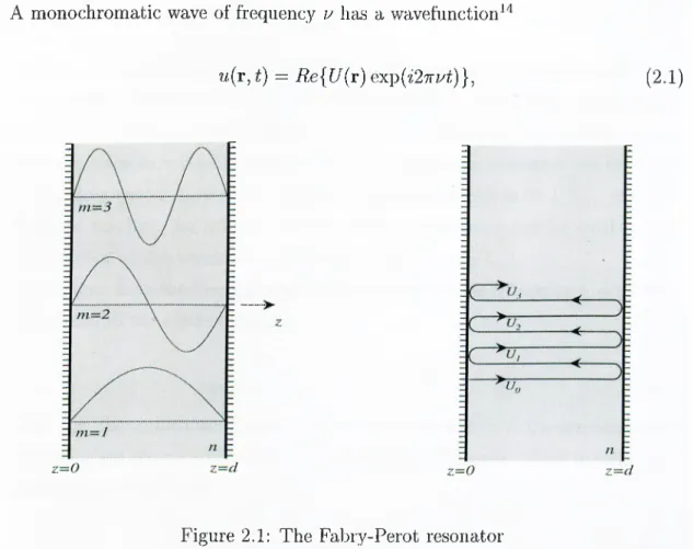
Fabrication and characterization of amorphous silicon microcavities
Tam metin
Şekil


Benzer Belgeler
Katakaumene’den Tauroslara kadar olan kısımlar o kadar iç içe geçmiştir ki Phrygialılar, Karialılar, Lydialılar ve Mysialılar birbirlerine karıştıklarından beri
An LED core may emit at various wavelengths spanning from ultraviolet to visible and infrared, depending on the electronic structure of the material which it is made
Figure 7.1.1 Luminescence spectrum of our hybrid system improved by using non- radiative energy transfer pumping of red-emitting CdSe/ZnS core/shell nanocrystals (λ PL =
%10’luk sodyum hipoklorid çözeltisi içerisinde farklı sürelerde sterilizasyona tabi tutulan soğanların tamamında %100 oranında deformasyon gözlenmiş olup,
1985-2005 yılları arasında yayımlanmış öykü kitaplarının eksiksiz bir listesinden oluşacak bu veri tabanı sayesinde, 1990’dan bugüne uzanan öykü pratiği
Using the TCP send rate formula provided in [ 9 ], we propose a nested fixed-point iterative algorithm to study a network of routers of arbitrary topology using CBWFQ-based schedul-
Bir fizik tedavi seansındaki bir ya da birden fazla egzersiz tipini algılamak için, temeli dinamik zaman bükmesi (DZB) benze¸smezlik ölçütüne dayanan bir
The I-V and admittance (C-V and G/w-V) measurements of the (Ni/Au)/AlGaN/AlN/GaN heterostructures were performed using a Keithley 2420 programmable constant current source and
