https://doi.org/10.1007/s10854-018-0297-1
The effect of the triangular and spherical shaped CuSbS
2structure
on the electrical properties of Au/CuSbS
2/p-Si photodiode
Murat Yıldırım1 · Adem Kocyigit2 · Adem Sarılmaz3 · Faruk Ozel3,4
Received: 11 September 2018 / Accepted: 26 October 2018 / Published online: 29 October 2018 © Springer Science+Business Media, LLC, part of Springer Nature 2018
Abstract
CuSbS2 (Chalcostibite) crystals were synthesized by the hot-injection method as triangular and spherical shaped structures. The crystals were inserted by spin coating technique as interfacial layers between Au metal and p-Si to investigate their electrical and photoresponse properties via I-V measurements under various light intensities. The XRD measurements were performed to show the crystalline structure of the spherical and triangular CuSbS2. The TEM images confirmed the triangular and spherical particle structures of the CuSbS2 crystals. The I-V measurements were performed under dark, 20–100 mW light intensities with 20 mW interval for spherical and triangular CuSbS2 photodiodes. In addition, diode parameters were extracted and discussed in the details. The results highlighted that triangular and spherical shaped structures have good photoresponse to the illumination and can be employed in the photodiode and photodetector applications.
1 Introduction
Chalcostibite (CuSbS2) is new kind of promising material for thin film solar cells as a good absorber because it has suitable band gap energy value between 1.3 and 1.5 for pho-tovoltaic applications and optical absorption coefficient of 104 cm−1 [1]. In addition, the CuSbS
2 is environmentally friendly, abundant, stable phase and cheap material [2, 3]. These properties of CuSbS2 make it optimum material for photovoltaic absorber [4, 5]. There are many papers with increasing trend about the CuSbS2 recently in the literature, and the papers usually aimed to employ CuSbS2 for opto-electronic applications [6–13]. Kang et al. [7] synthesized
CuSbS2 thin films by reactive co-sputtering technique and investigated physical properties. In addition, they fabricated solar cells by employing CuSbS2. Sivagami et al.[8] obtained CuSbS2 nanobrick thin films by the solvothermal method and confirmed the purity of the films and then investigated photoresponse behaviors. Dekhil et al.[13] synthesized CuSbS2 nanopowders by hydrothermal method and stud-ied by various instruments to see the compatibility of the CuSbS2 nanopowders for photovoltaic applications.
Many techniques have been performed to fabricate as film or particle form of the CuSbS2 such as spray pyrolysis [14], chemical bath deposition [15], SILAR [16], electrodeposi-tion [17] and hot-injection techniques [18]. Among them, hot-injection technique provides to obtain good crystalline structures and narrow size distribution [19]. Various shaped is really important because various forms of the CuSbS2 can help to improve the thin film solar cells or optoelectronic applications [20].
Metal and semiconductor contacts can be thought as optoelectronic applications because the light causes electron–hole pairs at the interface when hit the contact [21–23]. When the electrons and holes jump the barrier of the metal–semiconductor contact, there is an increase at the current values that pass through to the contacts. These prop-erties most of the time are used for photodiode or photode-tector applications [24, 25]. However, the absorption of the light is really important for light conversion efficiency of the contacts [26]. The CuSbS2 crystals structures can improve
* Murat Yıldırım
[email protected] * Faruk Ozel
1 Faculty of Science, Department of Biotechnology, Selcuk
University, 42030 Konya, Turkey
2 Engineering Faculty, Department of Electrical Electronic
Engineering, Igdir University, 76000 Igdir, Turkey
3 Faculty of Engineering, Department of Metallurgical Science
and Materials Engineering, Karamanoğlu Mehmetbey University, 70200 Karaman, Turkey
4 KaramanogluMehmetbey University, Scientific
and Technological Research and Application Center, 70200 Karaman, Turkey
the light absorption of metal–semiconductor contacts as an interfacial layer for photodiode and photodetector applica-tions [4]. In addition, the shape or structure of the CuSbS2 can affect the behaviors of these photodiode/photodetectors. The aim of this study is to compare and understand the vari-ous CuSbS2 structures how to affect the photodiode proper-ties of the metal–semiconductor devices.
In this study, we synthesized triangular and spheri-cal structures of the CuSbS2 by hot-injection method and inserted the structures as thin film form by spin coating technique between the Au metal and p-Si to fabricate Au/ CuSbS2/p-Si photodiodes. The obtained photodiodes were characterized and compared by XRD, TEM and I-V measure-ments under dark and various light illumination intensities.
2 Experimental details
Copper antimony sulfide nanostructures were synthesized using powder and liquid sulfur source by the hot-injection method. The spherical shaped CuSbS2 crystal synthesis was previously published by our group [27]. Triangular shaped CuSbS2 were synthesized according to a previously described procedure with slight modification [28]. To syn-thesize CuSbS2 nanostructures, typically, copper (II) acetate (1 mmol), antimony (III) chloride (1 mmol) and oleylamine (15 mL) were added to a 25 mL three-necked, round-bottomed flask with electromagnetic stirring under argon atmosphere at room temperature for 15 min. Then, freshly prepared S-precursor solution (0.26 mL 1-dodecanethiol (1-DDT) and 1.76 mL tert-dodecylmercaptan (t-DDT)) was injected rapidly into the hot reaction mixture under vigorous stirring, which resulted in an immediate color change of the
reaction solution to black. Next, the solution was heated to 240 °C and kept at this temperature for 30 min. and cooled down to room temperature. Finally, the nanostructures were precipitated adding a mixture of ethanol and toluene cen-trifuged at the rate of 3000 r/min for 1 min. The final black precipitate was washed with ethanol to remove residual thi-ols and acetates.
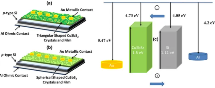
The (100) p-type Si wafer, which had 10 Ω cm, were cut 15 mm x 10 mm pieces and cleaned in acetone and propanol by an ultrasonic cleaner and then HF:H2O (1:1) solution was prepared and the wafer pieces immersed to the solution to remove impurities and native oxide layer from the sur-faces. Aluminum (Al) metal (99.999%) with a thickness of 150 nm was thermally evaporated from the tungsten filament onto the whole back surface of the wafer under a pressure of 2 × 10⁶ Torr. Then, a low resistivity ohmic contact was followed by a temperature treatment at 500 °C for 5 min in a N2 atmosphere. The prepared triangular and spherical of the CuSbS2 solutions were coated on glass and Si sub-strates by the spin coating technique at a spinning rate of 1200 rpm for 60 s with Fytronix SC-500 spin coater. The thickness measurement of the coated triangular and spheri-cal structures of the CuSbS2 thin films has been performed by stylus profilometer Veeco Dektak 150 and the thickness of triangular and spherical structures of the CuSbS2 have been determined as 214 nm and 232 nm respectively. In the end, Au layer which has an area of is 7.85 × 10⁻² cm−2 was evaporated on triangular and spherical shaped structures film surfaces as rectifying contact. So, Au/CuSbS2/p-Si devices were obtained, and schematic presentations of the devices have been shown in Fig. 1. In here, while triangular shaped CuSbS2 used device was called Au/T-CuSbS2 /p-Si, spherical shaped CuSbS2 crystal used device named as
Au/S-CuSbS2/p-Si. In addition, schematic energy band dia-gram of the device have been exhibited in Fig. 1c. The volt-age was applied to Au contact for measurements.
Powder X-ray diffraction (XRD) patterns were recorded with a Bruker D8 Advance X-ray (Cu α source with 1.5406 Wavelengths) diffractometer. TEM images were obtained on JEOL JEM-2100F transmission electron microscope (TEM) was used to take the nanostructure images of the crystals. I-V and the photovoltaic measurements were performed using by Fytronix FY-5000 photovoltaic characterization system under dark and various light illumination conditions.
3 Results and discussion
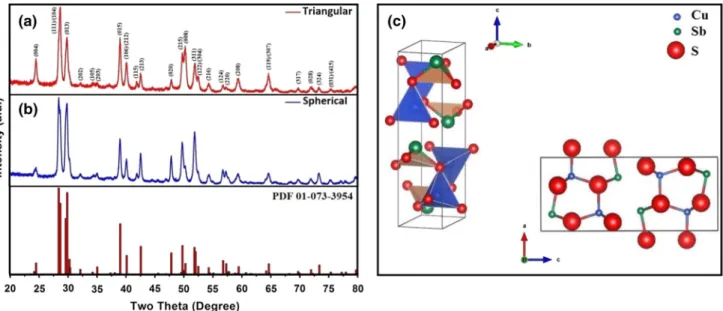
3.1 Structural propertiesX-ray diffraction (XRD) analysis was employed to identify the crystallographic structure and phase purity of the pre-pared chalcostibite samples in comparison with those of the triangular and spherical structured samples. The distinctive diffraction peaks for the CuSbS2 can be perfectly indexed as the single crystalline orthorhombic structures of CuSbS2 (PDF No: 01-073-3954) both spherical (Fig. 2a) and triangu-lar (Fig. 2b) shaped structure. Since the synthesized materi-als are of the same crystalline structure, both of the XRD patterns showed similar results [29]. However, as observed in Fig. 2a, b, the differences in peak intensities are due to dif-ferent interactions of the surfactants and anions. Moreover, there are no diffraction signals of binary structures on the XRD pattern, which showed that obtained nanostructures
had high purity. Figure 2c shows corresponding crystal structure with various directions as schematically.
3.2 Morphological properties
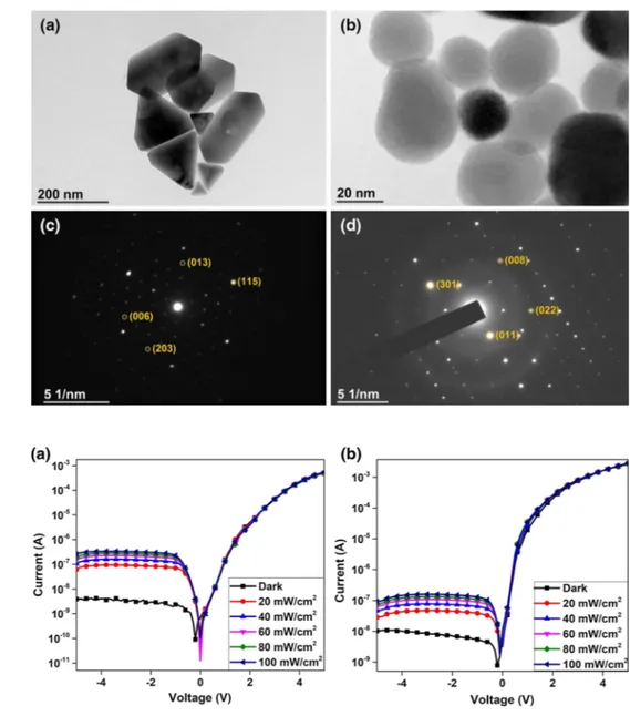
The TEM and SAED images of the T-CuSbS2 and S-CuSbS2 are presented in Fig. 3. According to Fig. 3a, T-CuSbS2 obtained by hot injection reaction mainly exhibits triangu-lar shape with edge lengths ranging from 20 to 120 nm. On the other hand, S-CuSbS2 exhibits a spherical structure with grain size ranges 20–40 nm, possessing a large surface area in Fig. 3b. The differences in the coordination capability of the products using OLA as solvents with the cations and anions could be the reason for the observed alterations in the shape and size of them. SAED images of the nanostruc-tures are given in Fig. 2c, d for T-CuSbS2 and S-CuSbS2, respectively. As presented in Fig. 2c, d, the nanostructures have single crystalline in nature. Further, SAED diffraction spots correspond to chalcostibite structure and these results are compatible with XRD results.
3.3 Electrical properties
The CuSbS2 crystals structure with triangular and spheri-cal shaped were employed as interfacial thin film layer to obtain Au/CuSbS2/p-Si devices. To characterize their elec-trical properties, I-V measurements were performed while the devices were under dark and illumination conditions in the range 20 mW-100 mW with 20 mW steps. The I-V characteristics of the Au/CuSbS2/p-Si devices have been shown in Fig. 4 for interfacial CuSbS2 layers with triangu-lar and spherical shaped structures. The devices exhibited
Fig. 2 XRD graphs of the CuSbS2 crystals a spherical, b triangular-shaped and c corresponding crystal structure with different directions as
good rectifying properties, but Au/S-CuSbS2/p-Si has bet-ter rectifying behavior than Au/T-CuSbS2/p-Si device. The obtained rectifying ratio values of the Au/T-CuSbS2/p-Si and Au/S-CuSbS2/p-Si devices are 1.37×10⁵ and 2.52×10⁵, respectively. The calculated rectifying ratio values are com-parable with literature [30, 31]. Both devices responded to the light illumination at reverse biases because the current values increased via increasing light intensity. This property caused by the generation of the electron–hole pairs in the interface of the devices owing to light illumination [32]. In addition, The devices can be employed as photodetector and photodiode applications because increasing current values at the reverse biases [33, 34].
The diode parameters can help to understand more the electrical properties of the devices. For that reason, the diode parameters such as barrier height (ϕb), ideality factor
(n) and series resistance (Rs) should be determined from
I–V measurements. There is three technique to calculate the
diode parameters: thermionic emission theory, Cheung and Norde methods. The current (I) is calculated from I-V meas-urements via the following formula according to thermionic emission theory [35–37]:
where I0 shows saturation current determined from the linear zone of the I–V graph. I0 also is calculated as the next equation:
where A, A* and T indicate diode area (in here A is equal to 7.85 × 10⁻³ cm2), Richardson constant (32 A cm−2 K−2
(1) I = I0exp( qV nkT )[ 1 − exp ( −qV nkT )] (2) I0=AA∗T2exp ( −q𝜙b kT )
Fig. 3 TEM and SAED images of the CuSbS2: a triangular,
b spherical shaped structures. SAED images of the c triangu-lar, d spherical shaped CuSbS2
crystals
Fig. 4 The I-V plots of a Au/T-CuSbS2/p-Si and b
Au/S-CuSbS2/p-Si devices under dark
for p-type Si) and temperature, respectively. q and k repre-sent the charge of electron and Boltzmann’s constant. The determined saturation current values for Au/T-CuSbS2 /p-Si and Au/S-CuSbS2/p-Si devices are 1.47 × 10⁻¹⁰ A and 2.75 × 10⁻¹⁰ A, respectively. While the saturation current help to calculate barrier height values, a slope of dV/dlnI provide to determine ideality factors of the devices for
V ≥ 3kT/q region via relevant formulas shown in below:
And
The ideality factors and barrier height values were accounted for and listed in Table 1 for Au/T-CuSbS2/p-Si and Au/S-CuSbS2/p-Si devices. While Au/T-CuSbS2/p-Si device has 6.96 ideality factor, the Au/S-CuSbS2/p-Si has 3.65 lower than triangular shaped CuSbS2 structures. The higher ideality factor values than one can be attributed to various reasons such as barrier inhomogeneity, distribution of the carriers, image force effects and series resistances of the devices [38–40]. The higher ideality factors at these devices can be attributed to barrier inhomogeneity and resistance effects [39, 41]. The differences at the ideality factor values between the Triangular-CuSbS2 and spherical-CuSbS2 devices confirmed the barrier inhomogeneity effect because triangular structure caused more non-uniform dis-tribution as an interfacial layer than particle structures. In addition, I–V characteristics of the devices were affected from the series (Rs) and shunt resistances (Rsh) which are
relevant with metal–semiconductor interfacial layer and semiconductor-contact interface, respectively, and they are called junction resistance (Rj) totally [42]. The determining
of these parameters is really important to understand the device characteristics [43]. The Rj is given as the following
equation:
The determined Rs and Rsh values were obtained as
82.2 kΩ and 4.56 × 10⁵ kΩ for Au/T-CuSbS
2/p-Si device, (3) n = q kT ( dV d ln I ) (4) 𝜙b= kT q ln ( A∗AT2 I0 ) (5) Rj= 𝜕V 𝜕I
2.95 kΩ and 1.34 × 10⁵ kΩ for Au/S-CuSbS
2/p-Si device. According to these results, both devices have higher Rsh
val-ues than Rs, and Rsh values are 108 Ω level. These results
made the devices ideal for high performance devices [44]. The conduction mechanism of the Au/T-CuSbS2/p-Si and Au/S-CuSbS2/p-Si devices should be determined by lnI-lnV plot because the thermionic emission theory is not effective for high n values. The relation between current and voltage is shown IαVm, and the m, power-law parameter is
determined from the slope of the linear region at lnI-lnV plot. Thus, the slope of the lnI-lnV plot refers to the con-duction mechanism of the junction. If the slope of the plots higher than two (m > 2), the space charge limited current (SCLC) mechanism is effective. If m is between one and two, Schottky and Poole–Frenkel Conduction are dominant. If m is equal to one, the junction has Ohmic character [45].
The lnI-lnV plots of the Au/T-CuSbS2/p-Si and Au/S-CuSbS2/p-Si devices have been shown in Fig. 5. While Au/S-CuSbS2/p-Si device has SCLC conduction mechanism, the Au/S-CuSbS2/p-Si device has Schottky and Poole–Fren-kel Conduction for first regions [22]. Poole–Frenkel Con-duction referred to that T-CuSbS2 layer started to conduct electricity. In the second and thirds regions of the Au/T-CuSbS2/p-Si and Au/S-CuSbS2/p-Si devices, the SCLC is dominant conduction mechanism and assigned to that the density of injected free charge is much larger than the
Table 1 The diode parameters of the Au/T-CuSbS2/p-Si and Au/S-CuSbS2/p-Si devices for various methods Device Saturation
cur-rent (I0)
n (I–V) n Cheung ϕb (I–V) (eV) ϕb Cheung
(eV) ϕb Norde (eV) R(kΩ (H(I)))s Cheung R[(kΩ (dlnI)]s Cheung Rs Norde (kΩ) Triangular shaped 1.75×10 −10 6.96 7.32 0.85 0.80 0.91 76.50 87.30 21.50 Spherical shaped 2.47×10 −10 3.65 4.60 0.83 0.90 0.83 6.18 8.75 6.07
Fig. 5 The lnI-lnV plots of Au/T-CuSbS2/p-Si and Au/S-CuSbS2/p-Si devices
thermal-generated free charge carrier density and increasing current [46].
The second method to calculate the diode parameter is Cheung method, and the method also helps to determine the
Rs values. Normally, all the time the metal–semiconductor devices have Rs, but we cannot calculate Rs values through
thermionic emission theory.
While Cheung method is performed, the current is written as the next equation including voltage drop at the current because of series resistance:
In this equation, IRs represent the voltage drop. While
the Rs is left alone at the left side of the Eq. (5), Cheung’s
functions are transformed to below formula:
where H(I) can be written as:
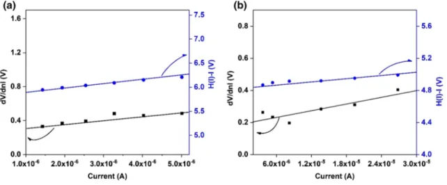
Equations (7) and (9) are called Cheung functions and derived by Cheung and Cheung [47]. While the graphs of Chung functions are plotted versus current, the graphs exhibit straight lines. The dV/dlnI versus I graph provides to determine ideality factor from y-intercept and series resist-ance value from slope. The H(I)-I graph is used to determine barrier height from y-intercept and another Rs value from
slope. The two Rs values is important for consistency of the
Cheung method [48]. (6) I = I0exp ( −q(V − IRs) nkT ) (7) dV d ln I =IRs+n kT q (8) H(I) = V − n( kT q ) ln( I AA∗T2 ) (9) H(I) = IRs+n𝜙b
Figure 6a, b show the dV/dlnI versus I and H(I) versus
I graphs of the Au/T-CuSbS2/p-Si and Au/S-CuSbS2/p-Si devices, respectively. The determined n, 𝜑b and Rs values are
listed in Table 1 for two devices. According to Table 1, there is some deviation both ideality factors and barrier heights of the devices. These differences can be ascribed to non-ideal diode structures, non-uniform distribution of the interface structures and approximation differences [48, 49]. Further-more, there are some differences also at the series resistance values for both devices obtained from dV/dlnI versus I and
H(I) versus I graphs because of barrier inhomogeneity or
native CuSbS2 layers. In addition, The obtained Rs values
is comparable Rs values through obtained Rj calculation for
both devices.
The alternative method to calculate the series resistance value, as well as barrier height, is Norde method. The func-tion of the Norde method is expressed as below equafunc-tion [50]:
where 𝛾 shows closest integer (dimensionless) value of the ideality factor, n. I(V) represents the currents depending on the voltages. If Eq. (10) is reorganized for 𝜑b and Rs, next
formulas are obtained:
where V0 is the minimum voltage value depending on
Norde function. Figure 7 displays F(V) versus V graphs of the Au/T-CuSbS2/p-Si and Au/S-CuSbS2/p-Si devices. The (10) F(V) = V 𝛾 − kT q ln ( I(V) AA∗T2 ) (11) 𝜙b=F(V0) +[ V0 𝛾 − kT q ] (12) Rs= 𝛾 −n I kT q
obtained 𝜑b and Rs values are tabulated in Table 1 for two
devices. According to 𝜑b values, Au/S-CuSbS2/p-Si device
has smaller 𝜑b than Au/T-CuSbS2/p-Si device. The reason
for this case can be attributed to non-uniform distribution of the triangular CuSbS2 structures at the interface layer of the device.
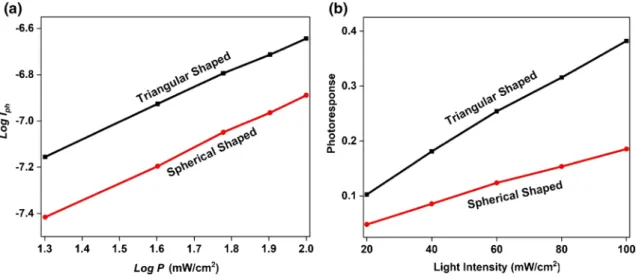
logIph versus logP plots of the devices have been
dis-played in Fig. 8a to understand the photoconductive mecha-nism. The below formula provide to understand the photo-conduction mechanism of the photodiodes.
where Iph, α, P m describe photocurrent, a constant, power
of the light and linearity ratio of light power-photocurrent, respectively. According to Fig. 8a, the Au/T-CuSbS2/p-Si (13)
Iph= 𝛼Pm
and Au/S-CuSbS2/p-Si devices have linear behavior with increasing light intensity and can be performed as photode-tector applications [51]. Figure 8b exhibits photoresponse graph of the Au/T-CuSbS2/p-Si and Au/S-CuSbS2/p-Si devices. Both devices again have linear photoresponse to the light.
4 Conclusions
We synthesized triangular and spherical shaped structures of the CuSbS2 crystals, separately and employed them as interfacial layer between the Au metal and p-type Si to fabri-cate Au/T-CuSbS2/p-Si and Au/S-CuSbS2/p-Si devices. The devices were characterized by XRD, TEM and I-V measure-ments. The XRD patterns revealed the crystal structure of the CuSbS2 for both triangular and spherical shaped struc-tures. The difference of two XRD patterns is just intensity changes of the plane peaks. The TEM images confirmed triangular and spherical shaped structure of the CuSbS2 and crystalline structure by SAED images. The I-V measure-ments were performed on the Au/T-CuSbS2/p-Si and Au/S-CuSbS2/p-Si devices under dark and various light intensities. The diode parameters of the devices were calculated and discussed in the details via comparing the devices. Accord-ing to diode parameters the spherical form of the CuSbS2 crystals is better than the triangular form of the CuSbS2. This result can be attributed to non-uniform distribution the triangular shapes of CuSbS2 in the interface of the device. The obtained devices can be employed as photodetector and photodiode applications.
Fig. 7 F(V)-V graphs of the Au/T-CuSbS2/p-Si and Au/S-CuSbS2 /p-Si devices
Acknowledgements This work is supported by Selçuk University BAP office with the research Project Number 17401159 and TUBITAK (The Scientific and Technological Research Council of Turkey) under project number 217M212.
References
1. B. Yang, L. Wang, J. Han, Y. Zhou, H. Song, S. Chen, J. Zhong, L. Lv, D. Niu, J. Tang, Chem. Mater. 26, 3135 (2014)
2. C. Macías, S. Lugo, Á Benítez, I. López, B. Kharissov, A. Vázquez, Y. Peña, Mater. Res. Bull. 87, 161 (2017)
3. L. Zhang, Y. Li, X. Li, C. Li, R. Zhang, J.J. Delaunay, H. Zhu, Nano Energy 28, 135 (2016)
4. S. Banu, S.J. Ahn, S.K. Ahn, K. Yoon, A. Cho, Sol. Energy Mater. Sol. Cells 151, 14 (2016)
5. M. Kumar, C. Persson, J. Renew. Sustain. Energy (American Insti-tute of Physics, College Park, 2013), p. 031616
6. R. Teimouri, R. Mohammadpour, Superlattices Microstruct. 118, 116 (2018)
7. L. Kang, L. Zhao, L. Jiang, C. Yan, K. Sun, B.K. Ng, C. Gao, F. Liu, Mater. Sci. Semicond. Process. 84, 101 (2018)
8. A.D. Sivagami, K. Biswas, A. Sarma, Mater. Sci. Semicond. Pro-cess. 87, 69 (2018)
9. U. Chalapathi, B. Poornaprakash, C.H. Ahn, S.H. Park, Ceram. Int. 44, 14844 (2018)
10. M.E. Edley, B. Opasanont, J.T. Conley, H. Tran, S.Y. Smolin, S. Li, A.D. Dillon, A.T. Fafarman, J.B. Baxter, Thin Solid Films 646, 180 (2018)
11. W. Wang, L. Hao, W. Zhang, Q. Lin, X. Zhang, Z. Tang, J. Mater. Sci. 29, 4075 (2018)
12. S. Moosakhani, A.A. Sabbagh Alvani, R. Mohammadpour, P.M. Hannula, Y. Ge, S.P. Hannula, Mater. Lett. 215, 157 (2018) 13. S. Dekhil, H. Dahman, S. Rabaoui, N. Yaacoub, L. El Mir, J.
Mater. Sci. 28, 11631 (2017)
14. J.A. Ramos Aquino, D.L. Rodriguez Vela, S. Shaji, D.A. Avel-laneda, B. Krishnan, Phys. Status Solidi 13, 24 (2016)
15. Y. Rodríguez-Lazcano, M.T.S. Nair, P.K. Nair, J. Cryst. Growth 223, 399 (2001)
16. Z. Liu, J. Huang, J. Han, T. Hong, J. Zhang, Z. Liu, Phys. Chem. Chem. Phys. 18, 16615 (2016)
17. A.C. Rastogi, N.R. Janardhana, Thin Solid Films 565, 285 (2014) 18. S. Ikeda, S. Sogawa, Y. Tokai, W. Septina, T. Harada, M.
Mat-sumura, RSC Adv. 4, 40969 (2014)
19. M.-R. Gao, Y.-F. Xu, J. Jiang, S.-H. Yu, Chem. Soc. Rev. 42, 2986 (2013)
20. K. Ramasamy, H. Sims, W.H. Butler, A. Gupta, J. Am. Chem. Soc. 136, 1587 (2014)
21. S. Wageh, W.A. Farooq, A. Tataroğlu, A. Dere, A.G. Al-Sehemi, A.A. Al-Ghamdi, F. Yakuphanoglu, Phys. B 527, 44 (2017) 22. B. Tatar, A.E. Bulgurcuoglu, P. Gokdemir, P. Aydogan, D.
Yilma-zer, O. ozdemir, K. Kutlu, Int. J. Hydrog. Energy 34, 5208 (2009)
23. I. Orak, M. Toprak, A. Turut, Phys. Scr. 89, 115810 (2014) 24. A.S. Dahlan, A. Tataroğlu, A.A. Al-Ghamdi, A.A. Al-Ghamdi,
S. Bin-Omran, Y. Al-Turki, F. El-Tantawy, F. Yakuphanoglu, J. Alloys Compd. 646, 1151 (2015)
25. F. Wang, J. Mei, Y. Wang, L. Zhang, H. Zhao, D. Zhao, ACS Appl. Mater. Interfaces 8, 2840 (2016)
26. O.S. Cifci, A. Kocyigit, P. Sun, Superlattices Microstruct. 120, 492 (2018)
27. M. Yıldırım, A. Aljabour, A. Sarılmaz, F. Özel, J. Alloys Compd. 722, 420 (2017)
28. A. Singh, H. Geaney, F. Laffir, K.M. Ryan, J. Am. Chem. Soc. 134, 2910 (2012)
29. F. Ozel, E. Aslan, B. Istanbullu, O. Akay, I. Hatay, Patir, Appl. Catal. B. 198, 67 (2016)
30. M. Soylu, I.S. Yahia, F. Yakuphanoglu, W.A. Farooq, J. Appl. Phys. 110, 074514 (2011)
31. E.A. Guliants, C. Ji, Y.J. Song, W.A. Anderson, Appl. Phys. Lett. 80, 1474 (2002)
32. B.A. Gozeh, A. Karabulut, A. Yildiz, F. Yakuphanoglu, J. Alloys Compd. 732, 16 (2018)
33. S.K. Singh, P. Hazra, S. Tripathi, P. Chakrabarti, Superlattices Microstruct. 91, 62 (2016)
34. O.S. Cifci, M. Bakir, J.L. Meyer, A. Kocyigit, Mater. Sci. Semi-cond. Process. 74, 175 (2018)
35. M. Ilhan, J. Mater. Electron. Devices 1, 15 (2017) 36. Ş Altındal, J. Mater. Electron. Devices 1, 42 (2017)
37. H. Özerli, İ Karteri, A. Bekereci, Ş Karataş, J. Mater. Electron. Devices 1, 83 (2017)
38. B. Roul, S. Mukundan, G. Chandan, L. Mohan, S.B. Krupanidhi, Cit. AIP Adv. Appl. Phys. Lett 5, 162111 (2015)
39. Ş Karataş, Microelectron. Eng. 87, 1935 (2010)
40. N.P. Maity, R. Maity, R.K. Thapa, S. Baishya, J. Nanoelectron. Optoelectron. 10, 645 (2015)
41. D.E. Yıldız, Ş Altındal, H. Kanbur, J. Appl. Phys. 103, 124502 (2008)
42. F. Yakuphanoglu, S. Actuators, A Phys. 141, 383 (2008) 43. L.D. Rao, V.R. Reddy, in AIP Conf. Proc. (AIP Publishing LLC,
2016), p. 120020
44. İ Taşçıoğlu, W.A. Farooq, R. Turan, Ş Altındal, F. Yakuphanoglu, J. Alloys Compd. 590, 157 (2014)
45. A. Kaya, E. Marıl, Ş Altındal, İ Uslu, Microelectron. Eng. 149, 166 (2016)
46. I. Missoum, Y.S. Ocak, M. Benhaliliba, C.E. Benouis, A. Chaker, Synth. Met. 214, 76 (2016)
47. S.K. Cheung, N.W. Cheung, Appl. Phys. Lett. 49, 85 (1986) 48. Ş Karataş, N. Yildirim, A. Türüt, Superlattices Microstruct. 64,
483 (2013)
49. A. Kocyigit, I. Orak, İ Karteri, S. Uruş, Curr. Appl. Phys. 17, 1215 (2017)
50. H. Norde, J. Appl. Phys. 50, 5052 (1979)