Nitrogen incorporation and optical studies of GaAsSbN / GaAs single
quantum well heterostructures
Kalyan Nunna, S. Iyer,a兲L. Wu, J. Li, and S. Bharatan
North Carolina A&T State University, Greensboro, North Carolina 27411, USA X. Wei
NHMFL Florida State University, Tallahassee, Florida 32310, USA R. T. Senger
Department of Physics, Bilkent University, 06800 Ankara, Turkey K. K. Bajaj
Department of Physics, Emory University, Atlanta, Georgia 30322, USA
共Received 19 March 2007; accepted 20 July 2007; published online 11 September 2007兲
In this work, the effects of N incorporation on the optical properties of GaAsSbN / GaAs single quantum wells 共SQWs兲 have been investigated using temperature, excitation, and magnetic dependencies of photoluminescence共PL兲 characteristics. These layers were grown in an elemental solid source molecular beam epitaxy system with a rf plasma N source. The N concentrations in the range of 0.5%–2.5% were investigated in this study. The SQW with N⬃0.5% exhibits a behavior similar to that in an intermediate regime where the contributions from the localized states in the band gap are dominant. The temperature and excitation dependencies of the PL characteristics indicate that for the N concentration of 0.9% and above, the alloy behavior is analogous to that of a regular alloy and the changes in optical properties are only marginal. The conduction band effective mass 共meff兲 values computed from the magnetophotoluminescence spectra using a variational formalism and the band anticrossing model are in good agreement and indicate enhanced values of meff. However, there is no significant variation in meffvalues of QWs for N艌0.9%. Small redshift of about 30– 50 meV for the temperature variations from 10 to 300 K in conjunction with unusually small blueshift observed in the excitation dependence of PL for N艌0.9% indicate that this system holds a great promise for laser applications at 1.55m and beyond. © 2007 American Institute of Physics.关DOI:10.1063/1.2777448兴
I. INTRODUCTION
The dilute nitride alloy quantum wells 共QW兲 lattice matched to GaAs currently under consideration for optical communications in the 1.3 and 1.55m wavelength regions are InGaAsN, GaAsSbN, and InGaAs共Sb兲N systems. The InGaAsN / GaAs has been established as a successful mate-rial system for laser device applications in the 1.3m re-gion. Extending the wavelength of operation to 1.55m in this alloy system dictates N and In concentrations exceeding 2% and 35%, respectively, resulting in considerable degrada-tion of the structural and optical properties.1–5However, ad-dition of Sb to this system allowed enhanced In incorpora-tion resulting in redshifting the wavelength further to 1.55m with improved material quality.1–5 Vertical cavity surface emitting lasers 共VCSEL兲 have been successfully demonstrated at 1.45m using this quinary system.5 How-ever, the presence of an additional component makes the system more complex.
GaAsSbN / GaAs system is another candidate that has shown great promise for application in this wavelength re-gion. Initial research work on these QWs were predomi-nantly carried out by Harmand and co-workers,6–8who dem-onstrated a band gap reduction of 180 meV in GaAsSb for a
N concentration of about 1%. Emissions as long as 1.57 and 1.35m were achieved in annealed GaAsSb0.15N0.025 and
GaAsSb0.25N0.01QWs,7,8respectively, though the former sys-tem exhibited poor luminescence efficiency. The low sys- tem-perature photoluminescence 共PL兲 characteristics in this sys-tem are reported7–12 to be dominated by localized excitons due to the N induced localized states and potential fluctua-tions. Different annealing techniques have been improvised by various groups1–13for the annihilation of N related states to improve the PL efficiency. Our recent work9,13 indicates that in situ annealing in an As ambient is more effective in the reduction of the density of localized states and nonradi-ative recombination centers that are responsible for PL ther-mal quenching. Room temperature 共RT兲 emission wave-length as long as 1.52m has been achieved14 in these in situ annealed QWs at relatively lower composition of N 共⬃1.4%兲 in comparison to those reported by Harmand et al.7,8
The conduction band 共CB兲 effective mass 共meff兲 in this system has been computed by Senger et al.15from the simu-lation of diamagnetic shift following a variational approach. The effective mass of the QW system with Sb and N com-positions of 30% and 1.5%, respectively, was calculated to be 00.9m0, almost 50% higher than in their reference GaAsSb system.
In this paper, we have carried out a detailed and system-atic study of the effect of N concentration 共0.5%–2.5%兲 on the structural and PL characteristics and their dependencies on temperature, incident laser excitation levels, and magnetic field in the in situ annealed GaAsSbN / GaAs single QW 共SQW兲 heterostructures. The values of meffhave been
calcu-lated utilizing the same variational formalism as in Ref. 15, assuming complete localization of holes. These values were compared to those estimated from the band anticrossing 共BAC兲 model. We find that the optoelectronic properties of these QWs are almost invariant with the N incorporation for 0.9% N and above.
II. EXPERIMENTAL DETAILS
The GaAsSbN / GaAs SQW structures were grown on undoped 共100兲 GaAs substrates by solid source molecular beam epitaxy共MBE兲 with elemental Ga/Al, As/Sb cracker and an rf generated N plasma sources. The GaAsSbN QW layer of about 90 Å was sandwiched between GaAs layers followed by GaAlAs to improve electron confinement in the QW. The growth temperatures of the QWs and GaAlAs bar-riers were 470 and 580 ° C, respectively, and these samples were exposed to Sb and As flux prior to QW growth. These were also subjected to in situ annealing in As ambient at 650 ° C for 10 min to improve the luminescence.13
High resolution x-ray diffraction 共HRXRD兲 was per-formed with a Bede Scientific Metrix-F automated diffracto-meter, equipped with a microsource x-ray generator. Second-ary ion mass spectroscopy共SIMS兲 measurements were also carried out using a Cs+primary ion beam with beam energy
of 1 – 3 KeV. The compositions of Sb 共28%–30%兲 and N 共0.5%–2.5%兲 were determined from the best fit simulations of the HRXRD spectra in combination with the SIMS analy-sis共details in Ref. 13兲. For reference, a GaAsSb SQW was also grown under similar conditions. The PL measurements were carried out using He–Ne laser as a light source for excitation and a 0.32 m double grating monochromator for wavelength dispersion with a liquid nitrogen cooled InGaAs detector. A closed cycle three stage APD cryogenic system was used to study the variation of the PL characteristics in the 10 to 300 K temperature range. Laser excitation depen-dence on these QW structures were performed in the range of 10– 326 mW excitation power.
Low temperature 共4 K兲 magnetophotoluminescence 共MPL兲 measurements were carried out with the magnetic field 共B兲 varying up to 32 T and directed normal to the sample. The details of the MPL setup are given in Ref.15.
III. RESULTS
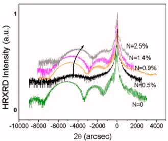
Figure 1 illustrates the HRXRD 共004兲 scan spectra of GaAsSbN SQWs for various N concentrations. With increas-ing N composition 共0.5%–2.5%兲, the QW layer peak shifts closer to the substrate peak as expected. Pendullosung fringes are observed in all the samples.
Figure2共a兲shows the variation of the Sb concentrations in the SQWs with the N incorporation. No significant change in the Sb concentration within the experimental error is ob-served for N concentrations up to 2.5%. The SIMS depth profile关Fig.2共b兲兴 indicates that the incorporation of both N and Sb in the QW layer begins at the same location, how-ever, the N profile terminates prior to that of Sb.
The PL peak energy decreases at the rate of 270 meV/ % N up to a N concentration of⬃1.4% and there-after the rate of reduction diminishes considerably, as dis-played in Fig. 3. The PL full width at half maximum 共FWHM兲 increases initially with N incorporation and re-mains invariant with further increase.
To get insight into the PL localized states and recombi-nation mechanisms, dependence of the PL peak energy on the temperature and laser excitation power at different N concentrations was carried out. Figures 4共a兲 and4共b兲 show the PL spectral variations with the temperature for the GaAsSbN SQWs of N⬃0.5% and 1.4%, respectively. The low temperature PL spectrum corresponding to N⬃0.5% ex-hibited a somewhat broad peak that could be resolved into a doublet about 35 meV apart, while in the rest of the samples,
FIG. 1. 共Color online兲 共004兲 HRXRD -2 scan spectra for GaAsSbN SQWs with increasing N concentration up to 2.5%.
FIG. 2.共Color online兲 共a兲 Variation of the Sb composi-tions in the SQW layers with N concentration varying up to 2.5%.共b兲 The SIMS depth profiles of the Sb and N incorporations in the GaAsSbN SQW with Sb ⬃30% and N⬃1.4%.
only a single peak is observed关Fig.4共b兲兴. The PL line shape is asymmetric at the lower temperatures exhibiting a long low energy tail, and it becomes more symmetric with in-creasing N concentration共though shown only for N⬃1.4%兲, as well as with measurement temperatures beyond⬃75 K.
The PL peak energy in the low temperature regime ex-hibits a共red-blue-red兲shift, as shown in Fig. 5共a兲. This is a characteristic S-curve behavior observed up to about 150 K in the dilute nitride material systems. With further increase in temperature, the PL peak energy decreases monotonically with temperature. The S-curve behavior is less pronounced for samples with higher N concentrations. The fit to the tem-perature dependence of the PL peak energy is obtained using Varshni’s empirical relation.9The fitting parameters, such as
␣ and  and the values of the exciton localization param-eters, such as Ttrans, Elocmax, Tdeloc, described in detail in Ref.
9, are listed in TableIand are shown in Fig.5共a兲. The values of the latter set of parameters decrease with an increase in the N concentration.
Figure5共b兲illustrates the corresponding temperature de-pendence of the total integrated PL intensity 共IPL兲 in these
SQWs. The intensity of the PL peak drops rapidly over two orders of magnitude with rise in the temperature above ⬃50 K. Excellent fit to the temperature dependence of the PL peak intensity data is obtained using a phenomenological expression given in Ref. 9, which assumes the presence of two nonradiative recombination channels. The activation en-ergies of the two different nonradiative channels Ea and Eb
and the ratio of the relative efficiency of these two nonradi-ative recombination mechanisms, A / B, for the different N concentrations are given in TableI.
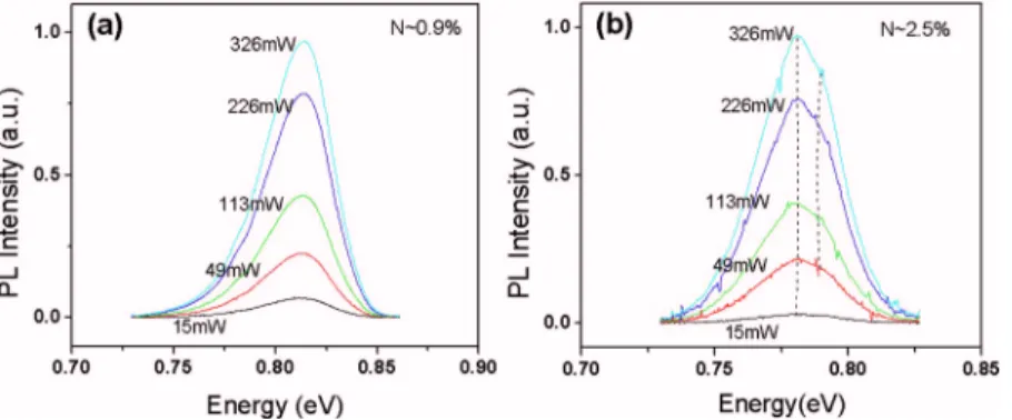
Figures6共a兲and6共b兲demonstrate the PL spectra at 10 K as a function of the laser power for the N concentrations of 0.9% and 2.5%, respectively. At low excitation levels, the PL line shape is asymmetric, with an exponential low energy tail being more pronounced for the QW of the lowest N concen-tration. The PL line shape becomes more symmetric with the increasing excitation power. For N艌1.4%, a shoulder evolves on the higher energy side of the emission peak 关shown in Fig. 6共b兲 for 2.5%N兴. A blueshift of ⬃11 meV is observed in the reference GaAsSb and drops to 0.4 meV for N艌1.4% with increase in the excitation power from 10 to 326 mW, as shown in Fig. 7.
Figures8共a兲and8共b兲 show the dependencies of the in-tegrated PL intensity and FWHM on incident laser power at different N concentrations. The integrated PL intensity is fit-ted using the power law of the form IPL= aPb, where IPLand
P are the integrated PL and laser intensities, respectively. The fitting parameters a and b are representative of the over-all PL efficiency and the nature of the recombination mecha-nisms, respectively. The FWHM of PL spectra of the GaAsSb QW increases with the laser power, while for N ⬃0.5%, it exhibits an opposite trend. For all the other N concentrations, the FWHM is found to be invariant with la-ser power.
Figure9 shows the variation of the diamagnetic shift ␦ defined as Eg共B兲−Eg共B=0兲, as a function of applied
mag-netic field for different N共0%–2.5%兲 concentrations. The dia-magnetic shift of the nitride QWs do not vary significantly with the N concentration and is less than half of that ob-served in the GaAsSb QW. The best fit simulations of these shifts have been performed using a variational approach with the CB electron mass as a fitting parameter and assuming the heavy-hole mass to be infinite, as in Ref.15. The meffthus
computed for the GaAsSb SQW is 0.05m0, which is
en-hanced to 0.070m0– 0.088m0 for the nitrides depending on
the N composition.
The above values are compared with those computed using the BAC model. Assuming the low temperature PL peak energy to be the band gap of the QWs, the experimental PL peak energy data for different N concentrations has been fitted using the following energy dispersion relation from the BAC model:16–18
Egp=EM共k兲 + EN−
冑
共EM共k兲 − EN兲2+ 4V2x
2 , 共1兲
where EN is the resonant energy level introduced by N, EM共k兲 is the interacting CB energy level of the host
semicon-FIG. 4.共Color online兲 PL lineshape dependence on the temperature in共a兲 N⬃0.5% and 共b兲 N⬃1.4% SQWs. FIG. 3. 共Color online兲 PL peak energy shift and FWHM variation at 10 K
ductor GaAsSb, V represents the coupling parameter be-tween the N states and the extended states, x is the nitrogen mole fraction. EN= 1.65 eV above the valence band edge,
and V is typically in the range of 2.4– 2.7 eV for GaAsN and InGaAsN material systems.16–18 The N energy level is as-sumed to be independent of the temperature as well as in the variation in the Sb composition. The BAC parameters of EN
and V of 1.65 and 3.9 eV, respectively, are found to provide a best fit to our PL peak energy variation with N%. These parameters were further confirmed by fitting the temperature dependence of the PL peak energy of the nitride QWs, where the temperature dependence of the host energy level was taken into account using our empirical values of␣and, as described earlier. Fitting with the BAC model is shown in Fig. 5共a兲 for one sample with N⬃1.4% only for clarity. It has to be noted that the BAC fitting did not include the QW with N⬃2.5%, as there is little band gap reduction with N% beyond N⬃1.4%. The meff values are then estimated from the following analytical expression derived from the disper-sion relation meff= m*
冋
1 +冉
Vx1/2 EN− EM冊
2册
, 共2兲where m*, the effective mass of the electron in the host GaAsSb, is taken to be 0.05m0 determined from the MPL
data discussed earlier. The meffvalues thus calculated from
the above approaches are compared in Fig.10.
IV. DISCUSSION
The presence of the Pendullosung fringes in the x-ray rocking curves of all the nitride QWs indicates sharp inter-faces and excellent crystalline quality of the grown layers 共Fig.1兲. With the increasing N concentration, the QW layer becomes more tensile strained as is evident from the shift of the QW peak towards the GaAs substrate peak. Sb
composi-tion was found to be relatively independent of the N incor-poration, consistent with the reports in the literature.5
The SIMS depth profiles in Fig. 2共b兲 indicates sharp buffer/QW interface in comparison to QW/cap layer. The Sb profile is broader than the N profile due to the trailing edge of Sb even after closing the Sb source shutter caused by the surfactant nature of Sb. Harris,5 on the contrary, found that both the N and Sb profiles do not begin as well as end at the same location in their GaAsSbN QW sample 共N⬃3% and Sb⬃10%兲. Hence, exposing the sample to As and Sb fluxes prior to the QW growth seems to improve the buffer/QW interface. This is also consistent with the results obtained using cross sectional transmission electron microscopy study of our samples, where the interface roughness was found to be smaller on the buffer/epilayer interface共0.3 nm兲 in com-parison to the epilayer/cap interface 共0.8 nm兲.19
The PL peak energy decreases at a rate of 270 meV/ % N for the N concentration varying up to 1.4%; thereafter, the variation is minimal, as shown in Fig. 3. The initial rapid band gap reduction with increasing N concentration in these QWs is commonly attributed20 to both the lowering of the conduction band as well as increase in the conduction band effective mass. The latter tends to saturate for N艌0.9% as discussed later, which partly accounts for the observed small rate of reduction in the PL peak energy. We have achieved a band gap reduction of ⬃328 meV for N⬃1.4% and Sb ⬃30% with respect to the GaAsSb 共30% Sb兲,21
while other groups observed a reduction of⬃230 meV for N⬃1.2% and
Sb⬃26%,6 ⬃196 meV for N⬃1.5% and Sb⬃30%,15
⬃155 meV for N⬃1%,3
and ⬃85 meV for N⬃0.7% and Sb⬃15%,8
with respect to their reference GaAsSb QW. Fur-ther, the energy reduction in our work is also relatively higher than those observed in the other dilute nitride sys-tems, namely, GaAsN: 290 meV for ⬃1.6%N,6 250 meV for N⬃1%18 from the host GaAs,18 InGaAsN:⬃314 meV for N⬃2.5%,2 ⬃180 meV for ⬃1.7% of N with respect to
TABLE I. Varshni’s parameters for the temperature dependence of the PL peak position and total integrated PL peak intensity for different N concentrations.
N% E10 K ␣ 共meV/K兲 共K兲 Eloc共10 K兲 共meV兲 Elocmax 共meV兲 Ttrans 共K兲 Tdeloc 共K兲 Ea 共meV兲 Eb 共meV兲 A / B 0 1.039 0.36 245 ¯ ¯ ¯ ¯ 24 5.1 23 0.5 0.932 0.28 100 30 62 90 165 26 7 37 0.9 0.823 0.37 273 6 16 75 100 22 5.2 42 1.4 0.786 0.36 325 4 8 60 90 26 7.6 42 2.5 0.788 0.33 204 9 9 10 80 22 4.9 10
FIG. 5.共Color online兲 Temperature dependence: 共a兲 PL peak energy and共b兲 integrated PL peak intensity of the
in situ annealed GaAsSbN / GaAs SQW heterostructures
for different N concentrations. The experimental data curve of N⬃2.5% in 共a兲 has been offset by 25 meV vertically for clarity. The superimposed solid curves are fits to the Varshni’s relation 共Ref. 9兲 and the open
circles are the fits using the BAC model. The dashed curves in共b兲 are the fitting curves 共fitting equation from Ref.9兲.
InGaAs,22 GaInNAsSb: ⬃50 meV for N⬃0.6% with refer-ence to GaInNAs,3 and⬃320 meV for ⬃1.5%N in GaSbN from the host GaSb.23 This stated range of band gap reduc-tion due to N is made based on similar composireduc-tions in both the non-nitride and nitride materials to get a better estimate of reduction due to N incorporation. Thus, the reduction in the band gap energy, with respect to the corresponding host non-nitride alloys, ranges from 105 to 250 meV/ % N in various dilute nitride III-V systems.2,3,6,8,15,18,22,23 It may be noted that, in comparison to other III-As based N alloys, the redshift in the emission wavelength is greater in Sb or mixed Sb–As based system. A similar conclusion has been drawn by Harmand et al.24where they report the reductions of 127, 124, and 151 meV% N contributions due only to N in the annealed GaAsN, InGaAsN, and GaAsSbN systems, respec-tively, relative to GaAs after carefully excluding the strain effects.
A 1.7m RT emission with a FWHM of 67 meV has been achieved for a SQW with N⬃1.4% and Sb⬃30%.21 RT emission of 1.53m with a FWHM of 45 meV has also been achieved on another in situ annealed SQW sample. These values are comparable to the best reported RT emis-sion “near” 1.5m of 35 meV at 1.48 m共Refs.3and24兲 but somewhat higher than 28.7 meV at 1.45m 共Ref. 4兲 after annealing in GaInNAsSb system.
The S-curve behaviors observed at low temperatures in the temperature dependence of the PL peak energy spectra of the GaAsSbN SQWs, as shown in Fig.5共a兲, are commonly attributed to the localized behavior of the excitons, due to the N induced potential fluctuations. This behavior has been dis-cussed in detail in our earlier work.9The maximum localiza-tion energy is unusually large共⬃62 meV兲 for 0.5%N sample and decreases drastically for higher N%. The localization energy defined as Eloc共T兲=Eg共T兲−EPL共T兲 at T=10 K is also
large 共30 meV兲 for N⬃0.5%, and, thereafter, it drops to 4 – 9 meV at higher N%. Likewise, Ttrans and Tdelocexhibit a
decrease with increase in N%. The behavior of the PL spec-trum of N⬃0.5% can be explained if the N concentration in this sample is considered to be in the intermediate dilute/ amalgamated region between the impurity and the regular alloy. In this intermediate regime, the PL spectrum consists of excitonic emissions bound to localized states below the band edge as well as from spatially distributed potential wells resulting in a broad spectrum. With a slight increase in temperature, the excitons bound to the localized potentials
in the temperature above Ttrans, the excitons are delocalized and the transitions from the conduction band start to take over, following Varshni’s relation. This high Elocmaxwas also witnessed in another sample with similar low N concentra-tion, which exhibited additional secondary peaks共not shown here兲. Hence, we do not believe it as a sample/growth based artifact. This is consistent with the observations in other ni-tride systems, such as GaAsN, where this transition region is reported to occur in the range of 0.4%–1.0%.25The PL line-shape is asymmetric for this sample with low energy tail longer, in comparison to the other nitride samples, which further attests to the assignment of dilute/amalgamated re-gion at this N concentration.
For N艌0.9% the values of Eloc共10 K兲 are comparable
to those reported in the InGaAsN QWs共Refs.10,11,26, and 27兲 but somewhat higher than those observed in the In-GaAsNSb QW 共Ref. 4兲 for similar N concentrations. How-ever, these comparisons have to be made with great caution, as the localization energy depends on the laser excitation intensity in addition to the material quality and N%. The decrease in Eloc共10 K兲 with N% is contrary to the
observa-tions of InGaAsN / GaAs QWs where it is found to increase with N%.26 The low values of Elocmax and Eloc 共10 K兲 for
N艌0.9% are clear evidence of shallow potential fluctuations in these samples. More symmetric PL line shape and the absence of a low energy tail in these samples further attest to the above inference.
FIG. 6.共Color online兲 PL lineshape dependence on the laser excitation power at 10 K for共a兲 N⬃0.9% and 共b兲 N⬃2.5%.
The above conjectures about the N dependence are also borne out in the excitation dependence of the FWHM and the blueshift observed in the PL peak energy. The linewidth of the PL emission exhibits an increase with laser excitation in the GaAsSb QW, as expected due to level filling in the tra-ditional alloys关Fig.8共b兲兴. On the other hand, in the case of N⬃0.5%, the PL linewidth shows a slight decrease with increasing laser power. This further supports the highly lo-calized nature of the states in this sample, as increase in the laser power would contribute to the population of bound ex-citons resulting in a narrower linewidth. At higher N%, no significant variation in the FWHM with a change in excita-tion level is observed. Further, the PL spectra at these high N concentrations can be resolved into two closely spaced peaks, separated by ⬃9 meV, similar to those observed by Saidi et al.28 in GaAsN epilayers. The absence of this addi-tional peak in the QWs with low N concentration suggests that this may be related to a modulation of the band struc-ture.
The values of b obtained from fitting the laser power dependence of the integrated PL intensity data are⬃1, sug-gesting the dominance of free exciton recombination 关Fig. 8共a兲兴. The values of the activation energies Eaand Ebfor the
nonradiative recombination channels, as determined from the temperature dependence of the integrated PL intensity are all similar.
The blueshift of the PL peak decreases with the N% for
the excitation power increase from 10 to 326 mW 共Fig. 7兲 and is ⬃0.4 meV for N艌1.4%. This shift is much smaller than the values of 18– 38 meV observed in GaAsN QWs 共Refs.29and30兲 and in InGaAsN QWs 共Ref.27兲 共extrapo-lated from the graphs in the mentioned references兲 for almost two orders of magnitude increase in excitation power. This again reflects the lesser potential fluctuations in our samples. This is also consistent with the smaller shift observed in the temperature dependence data. It is worth noting that the overall redshift from 10 to 300 K is in the range of 30– 50 meV for N艌0.9%, considerably smaller than those reported in the literature on the GaAsSbN / GaAs QWs and epilayers7,8,12,31and comparable to some of the lowest values reported for GaAsN共Refs. 28and32兲 and InGaAsN 共Refs. 11 and26兲 QWs and epilayers.
We have analyzed the variation of the low temperature PL transition energy with magnetic field共0–32 T兲. The dia-magnetic shift of this excitonic transition is calculated using the variational formalism as described in Ref. 15. In com-parison to the GaAsSb QW, the effect of incorporating small amounts of N is assumed to change only the electron effec-tive mass and the CB offset value.8 We have modeled the low temperature localization of the excitons in these QWs by assuming the heavy-hole mass to be infinite, and by treating the electron mass as an adjustable parameter. The value of 0.05m0 obtained for the GaAsSb QW is somewhat lower
than the reported value,15 which indicates that the
localiza-FIG. 8.共Color online兲 Integrated PL intensity data as a function of the laser excitation power for different N concentrations. The superimposed solid lines are the fits to the equation IPL共P兲=aPb to the experimental data.
共b兲 The corresponding variation of the FWHM with ex-citation power for different N concentrations.
FIG. 9.共Color online兲 The variation of the diamagnetic shifts as a function of magnetic field for the ternary and the quaternary SQWs grown at different N concentrations.
FIG. 10. 共Color online兲 The calculated values of meff as a function of N concentration from the diamagnetic shifts using the variational approach are compared with the corresponding values obtained from the BAC model.
tion of the excitons in our GaAsSb sample is weaker. Com-paratively lower diamagnetic shifts observed in the nitride QWs indicate an enhanced value of the electron effective mass in the GaAsSbN SQWs. The relatively larger value of meff calculated for the sample with 0.5% N can be
under-stood in view of the distinctly higher localization energy ob-served in Fig.5共a兲.
The calculated CB effective mass 共0.071m0兲 in the
GaAsSbN QW with 1.4%N is also slightly lower than that reported by Senger et al. 共0.090m0兲 共Ref. 15兲 in a similar QW with 1.5%N. In both the studies, the localization of ex-citons has been modeled with the assumption of perfectly localized holes, even though the actual physical origin of excitonic localization in these material systems is not com-pletely known. The type and degree of the localization can be related to the growth-dependent defect and the potential fluctuation profiles of a particular sample. It is to be noted that, from the diamagnetic shifts, one can only deduce that the exciton reduced mass information and the quantitative values of the meffcrucially rely on the assumed value of the hole effective mass. Perfect localization of the hole model provides a lower bound to the meffvalue. In the absence of
any reliable values of the localized hole masses in these alloy systems, this model at present provides the best estimate. However, the predicted relative enhancement of meffin the
nitride QWs共in the range of 40%–75% as a function of N concentration兲 should be far less sensitive to the choice of the heavy-hole mass value.
The meffvalues computed from the MPL data are found to be in good agreement with those determined from the BAC model. The value of EN= 1.65 eV that resulted in the
best fit to the experimental data is in excellent agreement
with the reported values in GaAsN and InGaAsN
systems.16–18However, the best fit value of the coupling con-stant V = 3.9 eV is considerably higher than the reported range of values of 2.4– 2.7 eV in the GaAsN and InGaAsN systems.16–18 The N level at ⬃1.22 eV was also considered based on the valence band edge in the GaAsSb共Sb⬃30%兲 共Ref.33兲 resulting in lower coupling constant of 2.8 eV, giv-ing equally best fit to the data for the PL peak energy varia-tion with the N% and temperature. Though the value of V is in excellent agreement with the reported data, the effective mass values calculated using these BAC parameters are found to be much higher than those computed from the MPL data. Thus, EN= 1.65 eV and V = 3.9 eV are considered to be
the BAC parameters that best describe the PL energy varia-tion with the N% and temperature in the GaAsSbN / GaAs SQWs. However, the high value of V = 3.9 eV cannot be ex-plained. It is well recognized that the BAC model does not take into account many of the effects, namely, interaction of the valence band as well as the density of states of the band tails on ENwhich may be important for the GaAsSbN / GaAs
system.
The above meffvalues determined from the BAC model
are found to be in good agreement with those computed from the MPL. However, in both the cases, there is not a signifi-cant variation among the m values of different nitride
V. CONCLUSIONS
In conclusion, the band gap reduction, effective mass, exciton localization energy at low temperatures, and the PL characteristics show only marginal changes in the in situ an-nealed GaAsSbN SQWs for N艌0.9%. The N dependent studies of the PL characteristics such as the peak energy, FWHM, and intensity with temperature and incident laser excitation indicate that 0.5%N corresponds to the dilute/ amalgamated region while N艌0.9% corresponds to that of a regular alloy. The CB effective mass values computed from the variational formalism as well as the BAC model are in good agreement. The temperature induced band gap redshift from 10 to 300 K is only 30– 50 meV, and the blueshift ob-served for the laser excitation increase by a factor of 32% is only 0.4 meV. These low values of shifts observed in this system make it a very attractive system for laser devices. Thus, this work indicates that this material system holds great promise for both extending the wavelength further and also for VCSEL devices operating in the 1.55m region.
ACKNOWLEDGMENTS
This work was supported by the Army Research Office 共Grant No. W911NF-04-1-0025兲. A partial funding for a stu-dent from The Penn State Electro Optics Center共Subcontract No. 0014-4-01150兲 is also acknowledged. One of the authors 共R.T.S.兲 acknowledges the financial support from TÜBA-GEBİP on the effective mass computations. The high resolu-tion x-ray diffracresolu-tion measurements were confirmed by Dr. Kevin Matney from Bede Scientific Inc, Englewood, Colo-rado. SIMS measurements were carried out at Evans Analyti-cal Group, New Jersey. The laser excitation and magneto-PL measurements were carried out at the National High Mag-netic Field Laboratory, Tallahassee, Florida.
1W. Ha, V. Gambin, S. Bank, H. Bae, M. Wistey, H. Yuen, S. Kim, and J.
S. Harris, Jr., IEEE J. Quantum Electron. 38, 1260共2002兲.
2K. Volz, V. Gambin, W. Ha, M. A. Wistey, H. Yuen, S. Bank, and J. S.
Harris, J. Cryst. Growth 251, 360共2003兲.
3L. H. Li, V. Sallet, G. Patriarche, L. Largeau, S. Bouchoule, L. Travers,
and J. C. Harmand, Appl. Phys. Lett. 83, 1298共2003兲.
4S. Bank, M. Wistey, L. Goddard, H. Yuen, V. Lordi, and J. S. Harris, Jr.,
IEEE J. Quantum Electron. 40, 6共2004兲.
5J. S. Harris, Jr., J. Cryst. Growth 278, 3共2005兲.
6G. Ungaro, G. Le Roux, R. Teissier, and J. C. Harmand, Electron. Lett. 35,
1246共1999兲.
7J. C. Harmand et al., J. Cryst. Growth 553, 227共2001兲. 8J. C. Harmand et al., Semicond. Sci. Technol. 17, 778共2002兲.
9J. Li, S. Iyer, S. Bharatan, L. Wu, K. Nunna, W. Collis, K. Bajaj, and K.
Matney, J. Appl. Phys. 98, 013703共2005兲.
10A. Pinault and E. Tournie, Solid-State Electron. 47, 477共2003兲. 11A. Pinault and E. Tournie, Appl. Phys. Lett. 78, 1562共2001兲.
12S. A. Lourenco, I. F. L. Dias, L. C. Pocas, and J. L. Duarte, J. Appl. Phys.
93, 4475共2003兲.
13L. Wu, S. Iyer, K. Nunna, J. Li, S. Bharatan, W. Collis, and K. Matney, J.
Cryst. Growth 279, 293共2005兲.
14L. Wu, S. Iyer, K. Nunna, S. Bharatan, J. Li, and W. J. Collis, Mater. Res.
Soc. Symp. Proc. 799, Z1.9.1-9.7共2004兲.
15R. T. Senger et al., Appl. Phys. Lett. 83, 5425共2003兲. 16C. Skierbiszewski et al., Appl. Phys. Lett. 76, 2409共2000兲.
19T. Biggerstaff, G. Duscher, S. J. Pennycook, N. G. Stoddard, and S. Iyer,
Philos. Mag.共submitted兲.
20R. Kudrawiec, G. Sek, K. Ryczko, J. Misiewicz, P. Sundgren, C. Asplund,
and M. Hammar, Solid State Commun. 127, 613共2003兲.
21K. Nunna, S. Iyer, L. Wu, S. Bharatan, J. Li, K. K. Bajaj, X. Wei, and R.
T. Senger, J. Vac. Sci. Technol. B 25, 1113共2007兲.
22H. Saito, T. Makimoto, and N. Kobayashi, J. Cryst. Growth 195, 416
共1998兲.
23T. D. Veal et al., Appl. Phys. Lett. 87, 132101共2005兲.
24J. C. Harmand et al., Dilute Nitride Semiconductors, edited by M. Henini
共Elsevier, San Diego, CA, 2005兲, Chap. 15, pp. 471–505.
25B. S. Ma, F. H. Su, K. Ding, G. H. Li, Y. Zhang, A. Mascarenhas, H. P.
Xin, and C. W. Tu, Phys. Rev. B 71, 045213共2005兲.
26J. Misiewicz, P. Sitarek, K. Ryczko, R. Kudrawiec, M. Fischer, M.
Rein-hardt, and A. Forchel, Microelectron. J. 34, 737共2003兲.
27E. M. Pavelescu, T. Jouhti, C. S. Peng, W. Li, J. Konttinen, M.
Dumi-trescu, P. Laukkanen, and M. Pessa, J. Cryst. Growth 241, 31共2002兲.
28F. Saidi, F. Hassen, H. Maaref, L. Auvray, H. Dumont, and Y. Monteil,
Mater. Sci. Eng., C C21, 245共2002兲.
29I. A. Buyanova, W. M. Chen, G. Pozina, J. P. Bergman, B. Monemar, H. P.
Xin, and C. W. Tu, Appl. Phys. Lett. 75, 501共1999兲.
30H. Dumont, L. Auvray, Y. Montiel, F. Saidi, F. Hassen, and H. Marref,
Opt. Mater.共Amsterdam, Neth.兲 24, 303 共2003兲.
31L. F. Bian, D. S. Jiang, P. H. Tan, S. L. Lu, B. Q. Sun, L. H. Li, and J. C.
Harmand, Solid State Commun. 132, 707共2004兲.
32H. Yaguchi, S. Kikuchi, Y. Hijikata, S. Yoshida, D. Aoki, and K. Onabe,
Phys. Status Solidi B 228, 273共2001兲.
33R. Teissier, D. Sicault, J. C. Harmand, G. Ungaro, G. Le Roux, and L.