Dependence of triboelectric charging behavior on material microstructure
Andrew E. Wang,1Phwey S. Gil,1Moses Holonga,1Zelal Yavuz,2H. Tarik Baytekin,2R. Mohan Sankaran,1and Daniel J. Lacks1
1Department of Chemical and Biomolecular Engineering, Case Western Reserve University, Cleveland, Ohio, USA 2UNAM-National Nanotechnology Research Center, Institute of Materials Science and Nanotechnology,
Bilkent University, 06800 Ankara, Turkey
(Received 26 April 2017; published 23 August 2017)
We demonstrate that differences in the microstructure of chemically identical materials can lead to distinct triboelectric charging behavior. Contact charging experiments are carried out between strained and unstrained polytetrafluoroethylene samples. Whereas charge transfer is random between samples of identical strain, when one of the samples is strained, systematic charge transfer occurs. No significant changes in the molecular-level structure of the polymer are observed by XRD and micro-Raman spectroscopy after deformation. However, the strained surfaces are found to exhibit void and craze formation spanning the nano- to micrometer length scales by molecular dynamics simulations, SEM, UV-vis spectroscopy, and naked-eye observations. This suggests that material microstructure (voids and crazes) can govern the triboelectric charging behavior of materials.
DOI:10.1103/PhysRevMaterials.1.035605
I. INTRODUCTION
Triboelectric charging describes the process by which two material surfaces become electrically charged after physical contact and separation [1]. Examples of triboelectric charging are ubiquitous, from useful technologies such as xerography [2] and energy harvesting devices [3], to undesired conse-quences such as damage to microelectronic device components [4], disruptions to industrial polymer processes [5] and agglomeration in pharmaceutical powders [6]. Triboelectric charging also appears in the natural environment, including dust storms and volcanic explosions [7] and has likely played a key role in the formation of planets [8] and the origin of life [9]. Despite having been a topic of study since antiquity [10], triboelectric charging remains largely unpredictable, with essentially no scientific understanding of even the most fun-damental aspects [1]. The most basic question in triboelectric charging is what determines the direction of charge transfer, i.e., which surface will charge negative and which positive when contacted. The current best approach for addressing this question is the “triboelectric series”, which refers to an ordering of materials in terms of their propensity to acquire positive or negative charge when contacted with another. However, this ordering of materials is completely empirical and cannot be correlated to any material properties [11–15]; the ordering is not universal and can depend on the nature of contact [16,17] and the processing history of the sample [18]; and even two chemically identical materials will transfer charge when contacted [19], which inherently contradicts the notion of a triboelectric series. There is now growing evidence that triboelectric charging involves subtle material chemistry that cannot be captured with one simple explanation [20–23]. Here, we introduce a new factor that can govern the direc-tion of charge transfer resulting from triboelectric charging: the material microstructure. To demonstrate, we carried out triboelectric charging experiments with polymer materials of identical chemical composition. When two samples of identical material are contacted symmetrically, the direction of charge transfer is random, as has been previously reported [24]. In contrast, we show that when one of the samples is permanently deformed, this sample behaves triboelectrically
like a distinct material; when the permanently deformed material is contacted with an undeformed material, there is systematic charge transfer in one direction just as would be expected if materials of different chemical composition were contacted. In addition to the triboelectric charging behavior, we examine the changes in microstructure resulting from deformation using a variety of characterization techniques and molecular dynamics simulations. We show that strain leads to the nucleation of voids on the nano- and microscale, and we argue that the altered microstructure produces the distinct triboelectric charging behavior.
II. METHODS A. Experiments
We focused our study on polytetrafluoroethylene (PTFE) because it is known to be one of the most electronegative materials (it typically charges negative when contacted with almost any material) and is very hydrophobic (and thus minimally affected by humidity and water adsorption) [25]. The as-purchased PTFE sheets (0.8-mm thickness, McMaster-Carr) are referred to as unstrained or 0% strain as no additional mechanical deformation was applied. The PTFE sheets were deformed by uniaxial tension using a MTS Electromechanical Universal Testing System (Criterion Series 43) at a rate of 25 mm/s. Samples were deformed to 100% of the initial length; this deformation is permanent, as the material does not relax back to the initial state when the stress is released. Both the 0% and 100% strain samples were cut to a final size of 63.5× 25.4 mm2for contacting studies to keep the area the same. Before contacting, samples were cleaned using acetone and methanol and allowed to dry for four minutes in ambient conditions.
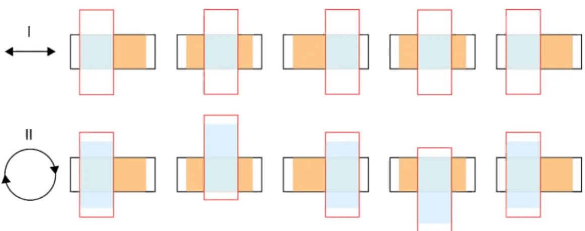
A mechanical apparatus was constructed to contact a pair of PTFE samples of varying strain. It is important to contact the two samples in a way that is symmetric, as an asymmetry in contact can lead to systematic charge transfer between the samples. As shown in Fig.1, we position the two rectangular samples perpendicular to one another. If we were then to translate one sample linearly back and forth over the other, the
FIG. 1. Comparison of two possible orientations of a pair of substrate samples for contact transfer experiments and resulting contact areas for charge transfer. In both cases, they are arranged one on top of the other, and the bottom sample is stationary while the top sample is moved. The area contacted on the bottom sample is shown in orange, and the area contacted on the top sample is shown in blue. In case I, the top sample is moved linearly back and forth across the bottom sample, leading to an unequal contact area for the two samples (see orange and blue shaded areas). In case II, the top sample is moved in a circular trajectory across the bottom sample, leading to an equal contact area for the two samples (see orange and blue shaded areas).
motion would be asymmetric in that the area of contact would be smaller on the moving sample than on the stationary sample. However, if we were to translate one sample in a circular trajectory (while maintaining perpendicular orientation) over the stationary sample then the area of contact would be the same on both samples. Thus we constructed a system that automatically contacts the samples in this circular manner, driven by a stepper motor. Contacting experiments were carried out at a rate of 22 cycles per minute for 90 seconds (this rate was the rotation rate of the stepper motor used in the apparatus; we do not think the specific rate would affect the results). The charge on each sample was measured, before and after contact, by placing the samples in a Faraday cup connected to an electrometer (Keithley 6517A). The net charge transferred on each sample was obtained as the difference in charge before and after contact.
Changes to optical properties of the samples resulting from strain were measured by ultraviolet-visible (UV-vis) spectroscopy (Shimadzu 1800) in the transmission mode. The reference (blank) spectrum was ambient air.
X-ray diffraction (XRD) was performed with a X-Pert Pro diffractometer at a step size of 0.0131◦ and a scan speed of 0.033667◦/s. Micro Raman spectroscopy was performed with a Witec Model Alpha 300S spectrometer using a 400-mW diode-pumped 532-nm solid state laser. The confocal microscope focused the laser to a spatial resolution of 200 nm. Scanning electron microscopy (SEM) was performed with a FEI Helios Nanolab 650. The system was operated at a low beam voltage of 350 V and images were acquired with multiple frames averaging to increase the signal to noise so that PTFE samples could be directly imaged without any conductive metal coating, in order to preserve the fidelity of the microstructure after straining.
B. Simulations
Molecular simulations were performed on PTFE. Although PTFE is typically semicrystalline [26], the molecular simula-tion of semicrystalline materials is extremely difficult, and we
believe the relevant changes are occurring in the amorphous phase—for these reasons, we carried out our simulations on fully amorphous PTFE. The simulations involved a system of 40 PTFE molecules, with each molecule consisting of 50 monomers. Periodic boundary conditions were used to remove surface effects and thus model a bulk system. The OPLS-AA force field was used to represent the potential energy of the system [27]. Electrostatic interactions were calculated using the particle-mesh-Ewald algorithm with a cutoff distance of 1 nm and a Fourier spacing of 0.4 nm [28], and Van der Waals interactions were considered up to a cutoff of 2 nm.
The amorphous PTFE system was generated by first inserting PTFE molecules into a large simulation box (15× 15× 15 nm3) without allowing them to touch each other. Molecular dynamics was then used in the NPT ensemble at high temperature (T = 1000 K) and pressure (P = 1 MPa) for 1 ns. To evolve the system to the appropriate density, the pressure was progressively increased in a series of 1-ns simulations until the appropriate density was obtained. The temperature was then reduced to 300 K, and the pressure was reduced to 1 atm, and an additional 40 ns simulation was used to relax the amorphous PTFE configuration at 0% strain. The molecular dynamics simulations were carried out using a leap-frog algorithm with a time step of 2 fs [29], and the temperature and pressure were controlled by a velocity-rescaling couple with a time constant of 10 fs [30], and a Berendsen couple with a time constant of 4 ps [31], respectively.
Axial strain was introduced by incrementally scaling the
z coordinate of each atom by a scaling factor, and then relaxing the system with a molecular dynamics simulation. These simulations allowed for the transverse dimensions of the material to contract as the material was strained axially; this is accomplished by NPT ensemble at atmospheric pressure with the compressibility in the z direction (βz) set to 0 to keep the axial strain constant. The compressibility in the x and y directions (βx,βy) was set to be 10−4MPa−1[32]. Four independent 40 ns simulations were run at each strain. Results were obtained for PTFE at{0%, 5%, 10%, . . . , 100%} strains.
We also simulated the straining of PTFE in the quasistatic limit in order to develop a physical understanding of the changes in structure with strain [33]. The quasistatic limit corresponds to the limit of zero temperature and zero-strain rate; this limit precludes all thermally induced or inertially induced dynamics, and during the trajectory the system thus remains at the nearest energy minimum. The quasistatic simulations are carried out by elongating the system in tiny increments, with the atom positions varied to minimize the energy after each strain increment. Each strain increment consisted of an axial extension of 0.1% and a perpendicular contraction in the appropriate amount as determined by the strain-dependent Poisson’s ratios from the thermal molecular dynamics simulations described in the previous paragraph. The energy minimizations were carried out using the conjugate-gradient algorithm, to the limits of machine precision.
All simulations were carried out using GROMACS/4.6
[34–37].AVOGADROandVISUAL MOLECULAR DYNAMICS
soft-ware were used for visualization [38,39]. III. RESULTS A. Stress-strain measurements
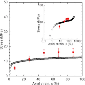
The experimental stress-strain curve of PTFE under tensile strain is shown in Fig. 2. For strains up to ∼2%, the deformation is elastic, such that stress increases linearly with strain; the Young’s modulus, given by the slope, is approximately 460 MPa. Above∼2% strain, yielding occurs which is characterized by a continual decrease in the slope of the stress-strain curve. Above∼100% strain, the material enters a strain hardening regime where the slope of the stress-strain curve again increases. The material fractures at
FIG. 2. Stress-strain measurements for PTFE films from experi-ments (red line) and simulations (open circles). Inset shows a log-log plot of the same data. Deformation of PTFE shows linear elastic (<2%), yielding (2%–100%), and strain hardening regimes (>100%).
about 400% strain. For strains beyond the elastic regime, the strain is irreversible, and the sample permanently remains in a strained state after the applied stress is removed. For our contact charging studies, we used samples deformed to 100% strain, such that the material has maximal inelastic deformation without entering the strain hardening regime.
Figure 2 also shows stress-strain results obtained from simulations at 300 K. The plastic flow stress observed in simulations is in reasonable agreement with experimental measurements. As the material is stretched axially, it contracts in the transverse dimensions; the magnitude of the contraction corresponds to a Poisson’s ratio of 0.45, which is close to literature values [40]. This agreement between the simulations and experiments supports our hypothesis that the mechanical properties are governed by the amorphous phase of PTFE.
B. Triboelectric charging experiments
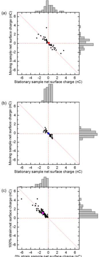
Figure 3(a) shows results for 40 contact charging ex-periments that were conducted between a pair of unstrained (0%) PTFE samples. The measurements show that in each experimental trial, one sample acquires a negative net charge and the complementary sample acquires a nearly equal positive net charge (thus falling on or close to the dashed line with a slope of –1). To assess experimental biases in charging behavior, such as whether the samples were moving or stationary, a statistical analysis of the data was performed. The mean charge was +0.11 ± 0.19 nC for the stationary sample, and+0.13 ± 0.18 nC for the moving sample; both of these mean charges are statistically indistinguishable from zero. Although the mean charges of both the moving and stationary samples were positive, we believe this is not a real effect and just due to noise as these charges were zero within the statistical uncertainty. Overall, the charging behavior is seemingly random, with no clear tendency for a given sample in an individual experiment to predictably charge negatively or positively, irrespective of whether the sample was moving or stationary. We note that there are some outlier data points with higher magnitudes of charging; these outliers could originate from random impurities on the surfaces, inhomogeneity in surface roughness that could lead to different contact area or different levels of bond breaking and material transfer, as well as other factors.
Results for 40 contact charging experiments between a pair of 100% strain samples are shown in Fig.3(b). Again, we find that samples charge negative and positive with approximately equal, but opposite charge in individual experimental trials (thus again falling on or close to the dashed line with a slope of –1). Interestingly, the span of charges measured is narrower for the pair of 100% strain than the 0% strain samples. A similar statistical analysis shows that for the stationary samples, the mean charge was +0.048 ± 0.091 nC, and for the moving samples the mean charge was –0.065± 0.093 nC; again, both of these mean charges are statistically indistinguishable from zero.
Finally, results for 80 contact charging experiments be-tween 0% strain and 100% strain samples are shown in Fig.3(c). In stark contrast to the contacting of equally strained samples, a very clear tendency is observed where the 0% strain sample charges negative and the 100% strain sample
FIG. 3. Summary of contact charging measurements for the following cases: (a) contact between two samples each at 0% strain; (b) contact between two samples each at 100% strain; and (c) contact between 0% strain sample and 100% strain sample. The net surface charges measured from each sample in the pair, defined as a difference between the surface charge before and after contact, are shown as a scatter plot and frequency histogram in each case.
charges positive with approximately equal, but opposite charge in each and every experimental trial (thus falling on or close to the dashed line with a slope of –1 but only in the top left quadrant). Importantly, statistical analysis showed that this charge dependency did not change whether the 0% strain or the 100% strain samples were moving or stationary. For the 100% strain samples, the mean charge was +1.2 ± 0.099 nC, and for the unstrained samples the mean charge was –1.2± 0.11 nC.
Our results thus show that the 0% and 100% strain PTFE samples have different triboelectric charging behaviors, such that when contacted, the 0% strain sample tends to charge negative and the 100% strain sample tends to charge positive. Thus strain appears to alter the material properties of the PTFE that control triboelectric charging.
FIG. 4. (a) Spectroscopic transmittance of 0% strain (black) and 100% strain (red) PTFE films. (b) Transmission of PTFE samples as a function of percent strain at 400 (blue), 550 (red), and 800 nm (black).
FIG. 5. Optical images of void formation and growth in strained PTFE films at (a) 250% strain, where the void is first noticed, (b) 350% strain, and (c) 417% strain, just before the void and film rupture. The diameters of the void are approximately 400, 700, and 1100 μm in (a)–(c), respectively.
C. Materials characterization
X-ray diffraction (XRD) and Raman spectroscopy were used to address potential changes to the chemical structure resulting from permanent deformation. The properties of 0% and 100% strain samples were compared (Fig. S1, Ref. [41]). We did not see significant differences in the XRD or Raman spectra, which indicated that the overall chemical structure did not appear to change significantly with strain.
The most salient change in the material resulting from strain is the opacity of the sample—the strained sample appears to the naked eye to be visibly whiter. This “strain whitening” is a well-known effect in polymer materials and is attributed to the formation of voids in the material that have sizes comparable to the wavelength of light (hundreds of nanometers) and thus scatter the light [42]. We quantified this effect spectroscopically. A comparison of transmission spectra collected for 0% and 100% strain PTFE samples between 350 and 800 nm shown in Fig. 4(a) confirms that the 0% strain samples have a higher transmittance than 100% strain samples. To illustrate this difference, the transmittance at 400, 550, and 800 nm are plotted as a function of strain in Fig.4(b), which more clearly shows that transmittance decreases with increasing percentage of strain.
Furthermore, we note that as the material is being strained, a small number of macroscopic holes become visible to the naked eye as the strain exceeds about 150%. As shown by a series of optical images collected from a PTFE sample while being deformed in Fig.5, the holes can be seen with the naked eye when they are about 300 μm in diameter [Fig.5(a)], and grow in size with increasing strain [Fig.5(b)], up to more than 1000 μm in diameter at strains that fracture occurs [Fig.5(c)]. The fracture of the material appears to be initiated from one of these holes.
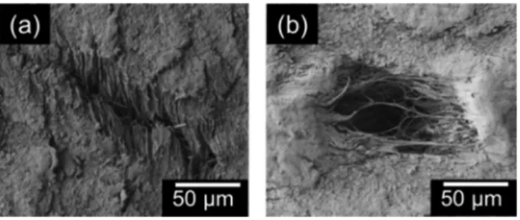
Some of the holes that are visible with the naked eye when the material is under tensile stress seem to “close-up” as the tensile stress is released, due to the small elastic contraction that occurs upon release of stress. We examined samples with SEM and found remnants of holes, as shown in Fig.6(a), as well as other smaller holes, approximately 50 μm in diameter, that were not visible with the naked eye, as shown in Fig.6(b). The SEM images reveal filamentary structure at the hole (fibrils) characteristic of crazing.
D. Molecular simulations
The molecular simulations show changes occur in the intramolecular structure with strain, in that the polymer chains
FIG. 6. Representative SEM images of PTFE films strained to fracture: (a) remnant of a void that was visible to the naked eye when under tension, but closed up when tension was released and (b) a void that was not visible to the naked eye.
stretch out and align in the direction of strain (Fig. S2, Ref. [41]). There are also slight shifts in the bond angle and torsion distributions with strain (not shown).
However, we believe the more important changes occur at longer nanometer scales. Above strains of about 50% the volume begins to increase significantly with strain. In comparison, at lower strains, the lateral contractions more closely balance the axial extensions to keep the volume roughly constant. The increase in volume is due to the formation and growth of voids in the material. Figure7shows snapshots of the system at strain increments of 10%; this is a view from the “top” of the simulation cell, and thus one cannot necessarily see what is happening in the interior (note also that there are periodic boundary conditions in all directions). Voids begin to form at strains of 50%, as evidenced by lighter-colored regions that imply that the top layers of atoms are missing. At 90% strain, a void spans the entire width of the simulation cell (the simulation cell is 4 to 5 nm wide).
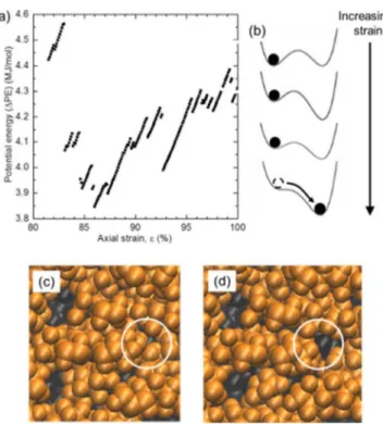
To investigate the mechanisms of void formation and growth, simulations were performed for deformation in the quasistatic (zero-temperature and zero-strain-rate) limit. In this limit, the system always remains in a local energy minimum. Results are shown in Fig. 8(a) for the potential energy as a function of strain. Usually, the potential energy increases continuously with increasing strain. However, there are numerous steps where the potential energy drops discon-tinuously. These changes are due to strain-induced changes
FIG. 7. Simulation results for microstructure of PTFE system as a function of strain.
FIG. 8. Results of quasistatic simulations: (a) potential energy as a function of strain in the inelastic deformation regime. (b) Schematic of changes in the potential energy landscape with strain; note the fold catastrophe where the energy minimum on the left disappears. (c) and (d) The molecular configuration just before (c) and just after (d) the discontinuous drop in potential energy at∼83% strain; note the structural change corresponds to the nucleation of a void, see a white circle.
in the potential energy landscape. Consider the schematic in Fig.8(b). As the system is strained slightly, the potential energy landscape is perturbed, but in the quasistatic limit, the system remains in the same potential energy minimum; such changes correspond to the continuous increases in potential energy with strain in Fig. 8(a). However, as shown in Fig. 8(b), eventually this potential energy minimum “disappears,” and at this point there are net forces that push the system to a different potential energy minimum; such changes correspond to the discontinuous potential energy drops in Fig.8(a). Our previous work has shown that the changes in characteristics of the potential energy landscape (barrier height, normal mode frequencies) follow the mathematical scaling behavior associated with fold catastrophes [33,43].
Following a fold catastrophe, the system relaxes to a dif-ferent energy minimum. We examined the structural changes associated with these atomic relaxations and find that in some cases these relaxations correspond to the formation and growth of voids [Figs. 8(c) and 8(d)]. Thus voids form and grow by sporadic discontinuous events as the system is strained, which correspond to fold catastrophes of the potential energy landscape.
IV. DISCUSSION AND CONCLUSIONS
Typically, in a pair of chemically identical material surfaces that are contacted symmetrically, triboelectric charging will occur such that one surface charges positive and the other
charges negative. However, which one of the two surfaces will charge positive and which negative will appear random [24], as demonstrated here in Figs.3(a)and3(b). We show here that when one of these PTFE samples is permanently deformed, there is systematic triboelectric charging such that the strained material almost always charges positive and the unstrained material almost always charges negative. This result is akin to charging behavior between materials with different chemical composition.
Why is the triboelectric charging behavior so dramatically altered when one material is permanently deformed? Previous work has suggested that large strain drives polymer systems into distinct amorphous states [44]. To assess structural changes to PTFE caused by deformation, we carried out XRD and Raman spectroscopy, but significant differences between the unstrained and strained PTFE were not observed. These methods probe the material structure at the molecular level, and thus we conclude that the molecular-scale structure of PTFE is not so significantly impacted by permanent deformation.
Instead, we suggest that the relevant structural changes caused by deformation are at a scale larger than the molec-ular scale, and correspond to the formation of voids. This idea is supported by the following: (1) molecular dynamics simulations which show the formation of voids of nanometer dimensions; (2) spectroscopic characterization which shows decreased transmittance arising from the scattering of light by voids that are the same length scale as the wavelength of visible light (hundreds of nm); (3) SEM analysis which reveals holes on the order of 50 μm diameter and smaller; and (4) the naked-eye observation of holes with diameters of a few hundred μm to over 1 mm. We note that the voids found by these four methods are on very different length scales, ranging from nanometers to a millimeter. We believe these voids are all related, as follows. Nanometer-sized voids are nucleated by plastic events [45,46] associated with fold catastrophes in the energy landscape [47]. These small voids grow and/or merge into larger voids on the order of hundreds of nanometers, which lead to scattering of light and decrease optical transmittance. Likewise, some of these voids in turn grow into the micrometer-sized voids observable by SEM, and some of those grow into macroscopic holes that can be observed by the naked eye.
The distinct triboelectric charging behavior found for permanently deformed samples could arise from the voids of a wide range of length scales, as well as the associated fibril structure (crazes). As noted, a correlation between triboelectric charging and material properties has yet to be established. In fact, it is not known whether charge transfer is due to the transfer of electrons, mobile ions, or radical moieties generated from the physical contact. The observed changes in the microstructure of the material could affect each mechanism of charge transfer: the electronic states near the voids and fibrils will likely be different from the rest of the material, which could lead to different electron transfer propensity; the different electronic states would lead to different ion adsorp-tion, which would in turn affect the transfer of adsorbed ions between surfaces; and the mechanical strength of the material could be weakened near the voids and fibrils to enhance ions, radicals, or larger fragments breaking off and transferring during rubbing. In addition, the presence of voids could lead to a different effective contact area at a smaller scale than the
overall contacting area of the sample surface (see Fig.1), and this asymmetry of contact areas could lead to different charging behavior.
ACKNOWLEDGMENTS
This material is based upon work supported by the National Science Foundation under grant numbers CBET-1235908,
CBET-1604909 and DMR-1206480. The calculations were carried out using computational resources through the Ohio Supercomputing Center. Z.Y. and H.T.B. are grateful for support from The Scientific and Technological Research Council of Turkey (TUBITAK project No. 214M358). We thank Richard Pham and Ross Widenor for their work on the early stages of this project.
[1] D. J. Lacks and R. M. Sankaran,J. Phys. D: Appl. Phys. 44, 453001(2011).
[2] C. B. Duke, J. Noolandi, and T. Thieret,Surf. Sci. 500,1005 (2002).
[3] S. Wang, L. Long, Z. L. Wang,Nano Lett.12,6339(2012). [4] J. E. Vinson and J. J. Liou,Proc. IEEE 86,399(1998). [5] G. Hendrickson,Chem. Eng. Sci. 61,1041(2006).
[6] K. C. Pingali, S. V. Hammond, F. J. Muzzio, and T. Shinbrot, Int. J. Pharmaceuticals 369,2(2009).
[7] T. Shinbrot and H. J. Herrmann, Nature (London) 451, 773 (2008).
[8] F. Spahn and M. Seiß,Nat. Phys. 11,709(2015).
[9] A. P. Johnson, H. J. Cleaves, J. P. Dworkin, D. P. Glavin, A. Lazcano, and J. L. Bada,Science 322,404(2008).
[10] P. Iversen and D. J. Lacks,J. Electrostat. 70,309(2012). [11] D. K. Davies,J. Phys. D: Appl. Phys. 2,1533(1969).
[12] Z. Sternovsky, M. Horányi, and S. Robertson, J. Vac. Sci. Technol. A 19,2533(2001).
[13] G. S. P. Castle,J. Electrostat. 40–41,13(1997).
[14] R. G. Horn, D. T. Smith, and A. Grabbe,Nature (London) 366, 442(1993).
[15] A. F. Diaz and R. M. Felix-Navarro, J. Electrostat. 62, 277 (2004).
[16] H. T. Baytekin, B. Baytekin, J. T. Incorvati, and B. A. Grzybowski,Angew. Chem. Int. Ed. 51,4843(2012).
[17] M. Sow, R. Widenor, A. Kumar, S. W. Lee, D. J. Lacks, and R. M. Sankaran,Angew. Chem. Int. Ed. 51,2695(2012). [18] P. E. Shaw,Proc. R. Soc. A 94,16(1917).
[19] J. Lowell and A. C. Rose-Innes,Adv. Phys. 29,947(1980). [20] B. Baytekin, H. T. Baytekin, and B. A. Grzybowski,J. Am.
Chem. Soc. 134,7223(2012).
[21] J. C. Angus, I. Greber, and K. Kash,J. Electrostat. 71, 1055 (2013).
[22] L. S. McCarty and G. M. Whitesides,Angew. Chem. Int. Ed.
47,2188(2008).
[23] C. Y. Liu and A. J. Bard,Nat. Mater. 7,505(2008).
[24] M. M. Apodaca, P. J. Wesson, K. J. M. Bishop, M. A. Ratner, and B. A. Grzybowski,Angew. Chem. Int. Ed. 49,946(2009). [25] Y. Awakuni and J. H. Calderwood,J. Phys. D: Appl. Phys. 5,
1038(1972).
[26] J. T. Shen, Y. T. Pei, and J. T. M. De Hosson,J. Mater. Sci. 49, 1484(2013).
[27] W. L. Jorgensen, D. S. Maxwell, and J. Tirado-Rives,J. Am. Chem. Soc. 118,11225(1996).
[28] U. Essman, L. Perera, M. L. Berkowitz, T. Darden, H. Lee, and L. G. Pedersen,J. Chem. Phys. 103,8577(1995).
[29] W. F. Van Gunsteren and H. J. C. Berendsen,Mol. Sim. 1,173 (1988).
[30] G. Bussi, D. Donadio, and M. Parrinello,J. Chem. Phys. 126, 014101(2007).
[31] H. J. C. Berendsen, J. P. M. Postma, W. F. van Gunsteren, A. Dinola, and J. R. Haak,J. Chem Phys. 81,3684(1984). [32] C. E. Weir,J. Res. Nat. Bur. Stand. 46,207(1951).
[33] Y. G. Chung and D. J. Lacks,J. Polym. Sci. Part B Polym. Phys.
50,1733(2012).
[34] B. Hess, C. Kutzner, D. van der Spoel, and E. Lindahl,J. Chem. Theory Comput. 4,435(2008).
[35] D. van der Spoel, E. Lindahl, B. Hess, G. Groenhof, A. E. Mark, and H. J. C. Berendsen,J. Comp. Chem. 26,1701(2005). [36] E. Lindahl, B. Hess, and D. van der Spoel,J. Mol. Mod. 7,306
(2001).
[37] H. J. C. Berendsen, D. van der Spoel, and R. van Drunen, Comput. Phys. Commun. 91,43(1995).
[38] M. D. Hanwell, D. E. Curtis, D. C. Lonie, T. Vandermeersch, E. Zurek, and G. R. Hutchison,J. Cheminform. 4,17(2012). [39] W. Humphrey, A. Dalke, and K. Schulten,J. Mol. Graphics 14,
33(1996).
[40] Properties Handbook (Teflon PTFE, DuPont, 1996).
[41] See Supplemental Material athttp://link.aps.org/supplemental/ 10.1103/PhysRevMaterials.1.035605for additional experimen-tal and simulation data.
[42] Y. Liu and R. W. Truss,J. Polym. Sci. B: Polym. Phys. 32,2037 (1994).
[43] C. E. Maloney and D. J. Lacks, Phys. Rev. E 73, 061106 (2006).
[44] G. B. McKenna,J. Phys.: Condens. Matter 15,S737(2003). [45] A. S. Argon,Acta Metall.27,47(1979).
[46] M. L. Falk and J. S. Langer,Phys. Rev. E 57,7192(1998). [47] D. L. Malandro and D. J. Lacks, Phys. Rev. Lett. 81, 5576