Research Article
Improving the Efficiency Enhancement of Photonic Crystal
Based InGaN Solar Cell by Using a GaN Cap Layer
T. F. Gundogdu,
1M. Gökkavas,
1and E. Ozbay
1,21Nanotechnology Research Center (NANOTAM), Bilkent University, 06800 Ankara, Turkey 2Department of Electrical and Electronics Engineering, Bilkent University, 06800 Ankara, Turkey
Correspondence should be addressed to T. F. Gundogdu; [email protected]
Received 2 May 2014; Revised 8 July 2014; Accepted 26 July 2014; Published 27 August 2014 Academic Editor: Sefer Bora Lisesivdin
Copyright © 2014 T. F. Gundogdu et al. This is an open access article distributed under the Creative Commons Attribution License, which permits unrestricted use, distribution, and reproduction in any medium, provided the original work is properly cited. We studied a high indium content (0.8) InGaN based solar cell design where the active InGaN layer is sandwiched between a GaN cap layer and a GaN spacer layer. The incorporation of the sacrificial cap layer allows for the etching of the front surface without removing the active InGaN resulting in a 50% enhancement of the short-circuit current density for a 15 nm-thick InGaN layer.
1. Introduction
One of the promising alternatives for the solution of the renewable energy problem is the development of solar cell technologies, where high energy-conversion efficiency is a
key requirement [1]. To date, silicon has been the solar
cell material of choice owing to its mature technology and comparably better availability. However, silicon, with a relatively small band-gap, has limited efficiency due to excess carrier energy generation and surface absorption. Alternative materials, mainly semiconductor compounds, have also been used in single or higher efficiency multijunction forms. Conventional high efficiency solar cell design relies on multiple junctions, each with differing band-gaps optimized in order to harvest energy from different portions of the solar irradiation. Theoretical studies show that increasing the number of junctions in a solar cell is an effective way of increasing efficiency. The practical number of junctions, on the other hand, is limited to a few due to the difficulty of growing and stacking dissimilar materials on top of each other without compromising material quality. Another limitation is the problem of current extraction from these heterostructures, where barriers between dissimilar materials have to be overcome for efficient current flow.
Following the development of the MOCVD (metal organic chemical vapor deposition) material growth tech-nology, the III-nitride material system has been utilized
in a number of key applications, such as lasers and LEDs (light emitting diode), UV (ultraviolet) photodetectors, and HEMTs (high electron mobility transistor). Historically, the material system incorporated only wide band-gap materials (AlN, GaN, and InN) limiting photonic device applications to the blue, UV, and deep-UV portions of the spectrum. When the band-gap of InN was recently revised to 0.7 eV
[2,3], allowing for band-gap tunable InGaN compounds, the
spectral range covered by InGaN-based heterostructures was effectively extended to include the photon energies between 3.7 eV and 0.7 eV, which coincides extremely well with desired optical absorption spectrum of multijunction terrestrial solar cells. Additional desirable properties of InGaN material
are well-established growth and fabrication processes [4],
the possibility of multiple-junctions within a single alloy
system, and high carrier mobility [5]. Together with the wide
absorption range and possibility of using thinner active layers allowed by a large absorption coefficient, InGaN has captured interest as an emerging candidate for next generation high efficiency cells. Furthermore, InGaN-based solar cells are particularly desirable for space applications because of their
superior radiation resistance [6]. Successfully demonstrated
cases of InGaN solar cells incorporate low concentration indium alloys, which results in absorption of a small spectral portion of the solar irradiation, ultimately limiting cell
con-version efficiency [7]. An increase in indium concentration
(e.g., to >25%) to capture a wider spectrum results in the
Volume 2014, Article ID 605204, 9 pages http://dx.doi.org/10.1155/2014/605204
detoriation of crystalline material quality. Epitaxial layers
with>25% In concentration have a critical InGaN thickness
on the order of a few tens of nanometers [8].
One method to increase the efficiency obtained from thin active layers of absorbing material is to excite guided mode resonances within these thin layers using nanophotonic
methods [9]. Solar cell structures incorporating
subwave-length modifications such as nanopatterned surfaces [10,11]
and backside gratings [12, 13], plasmonic nanostructures
[14, 15], embedded nanoparticles [16], and nanowires [17–
19] have been extensively reported. Similarly, there have
been a few reports in the literature on InGaN-based solar cells utilizing nanophotonic methods to increase efficiency. Embedded plasmonic nanoparticles were proposed in one study where calculations indicated 27% efficiency
enhance-ment [20]. Although it is possible to study such
embedded-type nanoparticles theoretically, in terms of experimental demonstration, nanostructures that are limited to material surface are more practical. An experimental work was pre-sented where metallic nanoparticles were deposited on an InGaN/GaN quantum well solar cell resulting in a 54%
increase in external quantum efficiency [21].
Another relatively easy to fabricate subwavelength sur-face modifications are photonic crystals. Photonic crystal enhanced solar cells aiming to enhance the efficiency of thin film solar cells by the mechanisms of optical path increase, light trapping, and optical impedance matching have been proposed and studied in the literature mostly for silicon and
germanium materials [22,23]. Our group has been working
on the growth of InGaN heterostructures [24–26]. Previously,
we proposed a solar cell design, where the optical absorption from a thin InGaN active layer was enhanced by a photonic
crystal etched into the top surface [27]. It was observed that
the etching away of the active InGaN material to fabricate the photonic crystal limited the achievable efficiency. In this work, we employ a GaN cap layer that serves to increase the enhancement achieved by the photonic crystal pattern. In the literature such capping layers have been proposed and demonstrated for a variety of device structures. The function of the cap layer is to improve either the electrical and/or the optical performance of the proposed device. In HEMTs, for example, the cap layer has multiple functions, to planarize/homogenize the surface, to increase the Schottky barrier height due to piezo polarization effects, to improve Ohmic contacts, and to passivate surface states. In LEDs and lasers incorporating InGaN quantum wells, GaN caps serve to homogenize and passivate the surface. To achieve pin structures, p-type GaN cap layers are employed in LEDs, lasers, and photodetectors. From an optical point of view, the GaN cap serves to displace the active layer from the surface. In the literature, the sandwiching of an absorbing material in nonabsorbing material is employed either to improve the absorption spectrum of photodetectors or to localize absorption within high E-field regions to improve bandwidth. Similarly, in lasers, nonabsorbing cap layers are employed as lossless waveguiding regions surrounding the high current areas. In this paper, the GaN cap layer is employed as a sacrificial layer that hosts the photonic crystal lattice structure, effectively displacing the active InGaN layer
to high optical field areas. Although the structure is not analysed electrically in this work, it is worth noting that the GaN cap layer can serve as a possible p-GaN contact layer as well.
2. Structure and Method
An initial design of layer structures studied in [27] is shown
inFigure 1(a). The thickness of the In0.8Ga0.2N active layer is
denoted by𝑑InGaN, and the thickness of a GaN layer beneath
the active layer is denoted by𝑑GaN. The epitaxial layers are
modeled to be grown on sapphire. Figure 1(c) depicts the
cross section of the proposed photonic crystal structure. The 1D photonic crystal structure is formed by etching trenches that have depth h and lattice constant a. The parameter b denotes the width of the photonic crystal grating, where the width of the trenches is equal to a-b. The graphic in
Figure 1(e)illustrates the perspective view of the proposed
design. In [27], we have shown that an optimized design of
the photonic crystal structure, inFigure 1(a), yields a
short-circuit current density increase of 17.5% for a case where
𝑑GaN = 200 nm and 𝑑InGaN = 150 nm. However, it was also
observed that the enhancement is limited since the etching of the photonic crystal pattern effectively removed a significant portion of the active absorber material InGaN. To alleviate this problem, we propose the modified layer structure as
shown in Figure 1(b). Here, the InGaN layer is displaced
from the surface and sandwiched between two GaN layers to facilitate the etching of the top GaN layer instead of the active InGaN layer. The thickness of the top GaN layer is denoted
by the parameter 𝑑GaN cap and the thickness of the bottom
GaN layer is denoted by the parameter𝑑GaN spacer. To achieve
a fair comparison among results of different structures, the
total thickness of the structure𝑑 = 𝑑InGaN +𝑑GaN=𝑑InGaN
+𝑑GaN cap +𝑑GaN spacer = 350 nm for all results reported in
this paper. When the modified layer structure inFigure 1(b)
is etched as shown in the cross section in Figure 1(d), the
resulting 3D geometry is as shown inFigure 1(f).
As discussed in [27], I-V (current-voltage) curve can
be used to express the electrical behavior of solar cells and the efficiency can be extracted by analyzing the I-V characteristics. By using the I-V curve descriptions for an
ideal diode as detailed in [28], it is possible to show that
there is an approximate linear relation between the solar cell
conversion efficiency and short-circuit current density 𝑗sc.
As a consequence, one can employ the short-circuit current density as a figure of merit without further elaborating the electrical behavior. If it is assumed that each carrier pair is transported to the circuit and the influence of the photonic
crystal structure is neglected,𝑗sccan be written as
𝑗sc = ∫
𝑑𝑗sc
𝑑𝜆𝑑𝜆 = 𝑒 ∫ 𝐴 (𝜆)
𝑑𝑁
𝑑𝜆𝑑𝜆. (1)
In the equation,𝐴(𝜆) is the spectral absorption and 𝑑𝑁/𝑑𝜆
is the photon flux density [27]. For terrestrial solar cells,
the integration starts at 280 nm as a result of the filtering in the ozone layer. The upper limit is determined by the
In0.8Ga0.2N dInGaN GaN dGaN Sapphire (a) In0.8Ga0.2N GaN GaN Sapphire dGaN cap dInGaN dGaN spacer (b) a b h GaN Sapphire (c) In0.8Ga0.2N a b h GaN Sapphire (d) (e) (f)
Figure 1: (a) Initial InGaN PC structure studied in [27]. (b) Layer structure of the modified solar cell structure incorporating the GaN cap layer. (c) Cross-sectional etch geometry for the initial structure in (a). (d) Cross-sectional etch geometry for the modified structure in (b). (e) 3D view for the initial structure in (a). (f) 3D view for the modified structure in (b).
is cut-off beyond 860 nm. For any studied structure type, the specific spectral absorption pertaining to each structure was calculated and weighted by the photon flux density to find the short-circuit current density. As the incoming radiation, the spectrum of a blackbody at 5800 K with a power density equal
to 1000 W/m2was used as a smooth replacement for the AM
1.5 G irradiation. To calculate the spectral absorption, finite-difference time-domain (FDTD) method was employed with periodic boundary conditions. The spectral dependency of
the GaN refractive index was modeled after [29,30], while the
InGaN refractive index was modeled using data from [31,32]
as described in [27].
3. Results
Parametric simulations were performed to maximize the short-circuit current density for the initial structure in
Figure 1(a)and the improved structure including the GaN
cap layer inFigure 1(b). The effect of the three parameters
a (lattice constant), h (etch depth), and FF (fill factor) (=b/a)
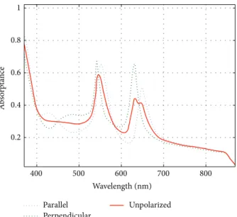
were investigated. As an example,Figure 2shows the
absorp-tion spectra for a 20 nm-thick InGaN layer sandwiched between a 130 nm-thick GaN cap layer and a 200 nm-thick GaN spacer layer, with the photonic crystal parameters of ℎ = 130 nm, 𝐹𝐹 = 50%, and 𝑎 = 300 nm, for the two orthogonal polarizations, as well as for unpolarized light. It is immediately observed that there are two peaks located close to 550 nm and 650 nm for both polarizations. The positions of the absorption peaks are slightly offset for the two polarizations and they shift towards larger wavelengths for longer periods, and their absolute value (height) depends
on the two parameters FF and h (see [27]). The highest𝑗scwas
observed when𝑎 = 300 nm. An increase or decrease from 𝑎 =
300 nm resulted in a slow decrease in 𝑗sc. To find the optimum
geometry, the short-circuit current density was calculated for
the parameter space spanned by FF and h. Figure 3shows
the result of this span for the 130 nm GaN-capped and
400 500 600 700 800 Wavelength (nm) Ab so rp ta n ce 0.2 0.4 0.6 0.8 1 Parallel Perpendicular Unpolarized
Figure 2: Calculated absorptance spectra for an optimized (FF = % 50, h = 130 nm, and a = 300 nm) solar cell structure with a 130 nm-thick GaN cap layer and a 20 nm-thick InGaN layer in the case of parallel (blue dotted), perpendicular (green dashed) polarizations with respect to the photonic crystal pattern, and unpolarized light incidence (solid red).
40 60 80 100 120 140 160 E tc h dep th (nm) 0 20 40 60 80 100 Fill factor (%) 2 3 4 5 6 7 8 jsc (mA/cm 2 ) (a) 40 60 80 100 120 140 160 E tc h dep th (nm) 0 20 40 60 80 100 Fill factor (%) 2 3 4 5 6 7 8 jsc (mA/cm 2 ) (b) 40 60 80 100 120 140 160 E tc h dep th (nm) 0 20 40 60 80 100 Fill factor (%) 2 3 4 5 6 7 8 jsc (mA/cm 2 ) (c)
Figure 3: Calculated short-circuit current density for an optimized solar cell structure with a 20 nm-thick InGaN layer and𝑎 = 300 nm. The incident light is (a) parallel and (b) perpendicularly polarized to the photonic crystal pattern. (c) For unpolarized illumination.
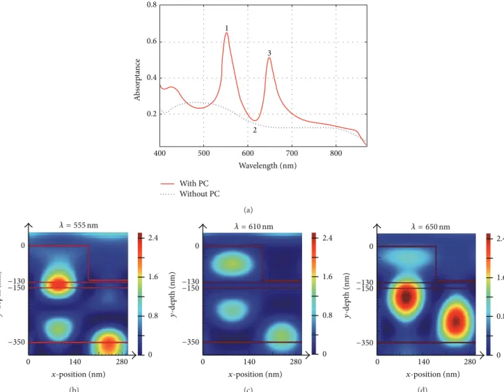
1 2 3 With PC Without PC 400 500 600 700 800 Wavelength (nm) Ab so rp ta n ce 0.2 0.4 0.6 0.8 (a) −350 −150 −130 0 y -dep th (nm) x-position (nm) 0 140 280 0 0.8 1.6 2.4 𝜆 = 555 nm (b) −350 −150 −130 0 y -dep th (nm) x-position (nm) 0 140 280 0 0.8 1.6 2.4 𝜆 = 610 nm (c) −350 −150 −130 0 y -dep th (nm) x-position (nm) 0 140 280 0 0.8 1.6 2.4 𝜆 = 650 nm (d)
Figure 4: Calculated absorptance spectrum and optical field intensity distribution for a solar cell structure with the following parameters: 20 nm-thick InGaN layer, 130 nm-thick GaN cap layer, 300 nm lattice length, 50% fill factor, and 120 nm etch depth. (a) Calculated absorptance. (b) Field distribution at 555 nm wavelength. (c) Field distribution at 610 nm wavelength. (d) Field distribution at 650 nm wavelength.
for light polarized parallel and perpendicular to the photonic
crystal trenches, respectively whereasFigure 3(c)illustrates
the case when the incoming light is unpolarized. It is observed that the short-circuit current density is maximized at (ℎ = 130 nm and 𝐹𝐹 = 60%) for light polarized perpendicular to the photonic crystal, at (ℎ = 130 nm and 𝐹𝐹 = 40%) for light polarized parallel to the photonic crystal, and at (ℎ = 130 nm and 𝐹𝐹 = 50%) for unpolarized light. It is seen that a reference structure without the photonic pattern (when
the fill factor is equal to 100%) results in a𝑗sc= 5.9 mA/cm2.
The calculated short-circuit current density for the optimum
structure is 8.38 mA/cm2, corresponding to a 42% increase
over a reference structure. The dependency of the parametric results around the optimum can be observed by inspecting
Figure 3. First, the maximum enhancement occurs at a
larger fill factor (but at the same etch depth) value for the perpendicular polarization in comparison with the parallel polarization. Second, as expected, for both polarizations,
the short-circuit current density drops quickly as the etch depth increases from the optimum value and the InGaN layer is removed.
Figure 4shows the calculated absorption spectra and the
associated optical field distribution for a solar cell structure with 130 nm GaN cap layer, 20 nm InGaN layer, 300 nm period, 50% fill factor, and 120 nm etch depth. In part (a)
ofFigure 4, the absorption spectrum of the PC-etched solar
cell (120 nm etch depth) and the absorption spectrum of the reference structure (no etch) are compared. It is observed that the PC pattern improves the absorption at two peaks located around 555 nm and 650 nm, while it does not significantly affect the absorption outside the peak regions. Parts (b),
(c), and (d) of Figure 4 show the optical field intensity
inside the photonic crystal etched solar cell structure for the three different wavelengths of 555 nm, 610 nm, and 650 nm, respectively. These wavelengths correspond to the points
400 300 500 600 700 800 900 Wavelength (nm) Ab so rp ta n ce 0.2 0.4 0.6 1 0.8 10 nm InGaN 20 nm InGaN 50 nm InGaN 100 nm InGaN
Figure 5: Calculated absorptance spectra for optimized GaN-capped solar cell structures with 10 nm (blue), 20 nm (green dashed), 50 nm (red dotted), and 100 nm-thick (light blue dot-dashed) InGaN layers.
the etched structure, as well as the boundaries between differ-ent layers, is shown for clarity purposes. The top surface of the
structure is located at𝑦 = 0, while the active InGaN layer is
placed between𝑦 = −130 nm and 𝑦 = −150 nm. Parts (b) and
(d) ofFigure 4show significant enhancement for the optical
field within the InGaN layer at the absorption peaks, while
it is observed inFigure 4(c)that the field is not enhanced
at all within the InGaN layer for this wavelength between the peaks. In the literature, the photonic crystal in this work is explained by relating it to a diffraction grating, where normally incident light is diffracted in oblique directions, resulting in a longer path and associated higher absorption. A wave optics explanation would be that the grating couples light into and excites guided slab modes. The existence of diffracted light and resulting Fabry-P´erot resonances in the structure shapes the absorption spectrum. Deeper trenches modify the slab waveguide modes to photonic crystal modes and the resulting absorption peaks are more pronounced.
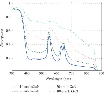
Figure 5shows the calculated absorption spectra of the
modified GaN-capped structure inFigure 1(d)for different
values of the InGaN layer thickness. The etch depth and fill factor are chosen to maximize the absorption of the
unpolarized light. For all four curves inFigure 5, the shape
of the spectral absorption is qualitatively similar with two distinct high absorption regions that are located between 500 to 600 nm and 600 to 700 nm. As the InGaN thickness increases, the absorption peaks broaden and their height above the baseline decreases in contrast to an increase in total absorption outside the peak regions. This result indicates that the enhancement by the photonic crystal pattern is more prononunced in the wavelength region of the two peaks and the absolute value of the enhancement is higher for thinner InGaN layers.
To compare the short-circuit current densities obtained
from the initial design shown inFigure 1(c)and the modified
design shown inFigure 1(d), calculations were performed for
a range of InGaN layer thickness values. For all calculations,
the period𝑎 = 300 nm was chosen, and the etch depth ℎ
and fill factor were optimized to maximize the short-circuit current density for unpolarized light. In the case of the
GaN-capped structure ofFigure 1(d), the thickness of the top GaN
layer was chosen as another free parameter and optimized
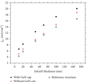
separately for each InGaN layer thickness.Figure 6 shows
the calculated𝑗scversus InGaN layer thickness for the initial
design without the GaN cap (as shown inFigure 1(c)), the
modified design with the GaN cap (as shown inFigure 1(d)),
and a reference structure (unetched as shown inFigure 1(b)).
It can be seen that for all InGaN layer thicknesses, the incorporation of the GaN-cap layer, i.e., the placement of the InGaN active layer away from the surface resulted in higher current densities. This is expected; since in order to form the photonic crystal pattern, the active InGaN layer is being etched away for the conventional design, whereas, in comparison, only GaN sacrificial cap layer is being etched away for the case of the improved design with the GaN cap layer. Therefore, it is possible to obtain higher current densities with thinner InGaN layers by using the improved
design with the GaN cap layer shown inFigure 1(d).
As discussed earlier, it is desirable to design solar cells incorporating InGaN layers thinner than the critical
thick-ness for any given InGaN composition.Figure 7shows the
maximum attainable enhancement over a reference structure without any photonic crystal pattern for both the initial design where the thin InGaN layer is placed at the top surface and the improved design where the thin InGaN layer is sandwiched between two GaN layers. It can be seen that the enhancement is higher for the modified design with the sacrificial GaN cap layer compared to the design where the active InGaN layer is placed at the surface without the GaN cap. In the case with the GaN cap, the enhancement
2 4 6 8 10 12 14 16 18 20 22 InGaN thickness (nm) 0 20 40 60 80 100 120 140 160
With GaN cap Without GaN cap
Reference structure
jsc
(mA/cm
2)
Figure 6: Calculated short-circuit current density versus the InGaN layer thickness demonstrating the improvement as a result of the structure design incorporating the GaN cap layer. Comparison between the improved structure with the GaN cap layer inFigure 1(d), the initial structure without the GaN cap layer inFigure 1(c), and the reference structure shown inFigure 1(b).
InGaN thickness (nm)
0 20 40 60 80 100 120 140 160
With GaN cap Without GaN cap
5 10 15 20 25 30 35 40 45 50 55 Enha ncemen t (%)
Figure 7: Calculated short-circuit current density enhancement versus the InGaN layer thickness demonstrating the improvement as a result of the structure design incorporating the GaN cap layer.
is as high as 50% for InGaN layers thinner than 15 nm and gradually drops as the InGaN layer thickness is increased. In the case of the design without the GaN cap, the maximum attainable enhancement is around 20%, achieved by very thin and thick (150 nm) InGaN layers. For thin layers, this result is readily understood, since the current density of the reference structure is lower for thinner layers. As the InGaN layer thickness gets higher, for equal amount of InGaN being etched away, the unetched portion of InGaN increases,
resulting in the enhancement increase between 70 nm and 150 nm. Of course, such a problem does not exist for the GaN-capped design, where only GaN material is etched away and, as a result, the maximum attainable enhancement is always higher than the enhancement attainable without the GaN cap, regardless of the InGaN layer thickness.
In conclusion, the spectral absorption and the short-circuit current density for an InGaN-based solar cell layer structure was calculated, the effect of a photonic crystal
surface pattern was investigated, and a sacrificial GaN cap layer was proposed to improve the enhancement of short-circuit current, and it was demonstrated that it is possi-ble to increase the current as much as 50%. This enhancement was obtained by the inclusion of the GaN cap layer which was removed during the surface patterning instead of the absorbing InGaN layer being etched in earlier designs. As an improvement to the current design, antireflective coatings and backside reflectors would further increase the enhance-ment. As the InGaN growth and fabrication technologies continue to mature, the proposed surface pattern designs can be employed to demonstrate practical solar cells with higher conversion efficiency.
Conflict of Interests
The authors declare that there is no conflict of interests regarding the publication of this paper.
Acknowledgments
This work is supported by the projects DPT-HAMIT, ESF-EPIGRAT, NATO-SET-181, and TUBITAK under the Project nos. 107A004, 107A012, and 109E301. One of the authors (E. Ozbay) also acknowledges partial support from the Turkish Academy of Sciences.
References
[1] J. Nelson, The Physics of Solar Cells, Imperial College Press, London, UK, 2003.
[2] J. Wu, W. Walukiewicz, K. M. Yu et al., “Small band gap bowing in In1−𝑥Ga𝑥N alloys,” Applied Physics Letters, vol. 80, no. 25, pp. 4741–4743, 2002.
[3] T. Matsuoka, H. Okamoto, M. Nakao, H. Harima, and E. Kurimoto, “Optical bandgap energy of wurtzite InN,” Applied
Physics Letters, vol. 81, no. 7, pp. 1246–1248, 2002.
[4] B. Butun, J. Cesario, S. Enoch, R. Quidant, and E. Ozbay, “InGaN green light emitting diodes with deposited nanoparti-cles,” Photonics and Nanostructures—Fundamentals and
Appli-cations, vol. 5, no. 2-3, pp. 86–90, 2007.
[5] Y. Nanishi, Y. Saito, and T. Yamaguchi, “RF-molecular beam epitaxy growth and properties of InN and related alloys,”
Japanese Journal of Applied Physics, vol. 42, no. 5A, pp. 2549–
2559, 2003.
[6] J. Wu, W. Walukiewicz, K. M. Yu et al., “Superior radiation resis-tance of In1−𝑥Ga𝑥N alloys: full-solar-spectrum photovoltaic material system,” Journal of Applied Physics, vol. 94, no. 10, pp. 6477–6482, 2003.
[7] O. Jani, I. Ferguson, C. Honsberg, and S. Kurtz, “Design and characterization of GaN/InGaN solar cells,” Applied Physics
Letters, vol. 91, no. 13, Article ID 132117, 2007.
[8] C. A. Parker, J. C. Roberts, S. M. Bedair, M. J. Reed, S. X. Liu, and N. A. El-Masry, “Determination of the critical layer thickness in the InGaN/GaN heterostructures,” Applied Physics Letters, vol. 75, no. 18, pp. 2776–2778, 1999.
[9] C. Heine and R. H. Morf, “Submicrometer gratings for solar energy applications,” Applied Optics, vol. 34, no. 14, pp. 2476– 2482, 1995.
[10] S. B. Mallick, M. Agrawal, and P. Peumans, “Optimal light trapping in ultra-thin photonic crystal crystalline silicon solar cells,” Optics Express, vol. 18, no. 6, pp. 5691–5706, 2010. [11] L. L. Yang, Y. M. Xuan, and J. J. Tan, “Efficient optical absorption
in thin-film solar cells,” Optics Express, vol. 19, no. 5, pp. A1165– A1174, 2011.
[12] J. Gjessing, E. S. Marstein, and A. Sudbø, “2D back-side diffraction grating for improved light trapping in thin silicon solar cells,” Optics Express, vol. 18, no. 6, pp. 5481–5495, 2010. [13] L. Zeng, Y. Yi, C. Hong et al., “Efficiency enhancement in Si solar
cells by textured photonic crystal back reflector,” Applied Physics
Letters, vol. 89, Article ID 111111, 2006.
[14] K. R. Catchpole, S. Mokkapatia, F. Becka et al., “Plasmonics and nanophotonics for photovoltaics,” MRS Bulletin, vol. 36, no. 6, pp. 461–467, 2011.
[15] S. Pillai, K. R. Catchpole, T. Trupke, and M. A. Green, “Surface plasmon enhanced silicon solar cells,” Journal of Applied Physics, vol. 101, no. 9, Article ID 093105, 2007.
[16] J. R. Nagel and M. A. Scarpulla, “Enhanced absorption in optically thin solar cells by scattering from embedded dielectric nanoparticles,” Optics Express, vol. 18, no. 13, pp. A139–A146, 2010.
[17] E. Garnett and P. Yang, “Light trapping in silicon nanowire solar cells,” Nano Letters, vol. 10, no. 3, pp. 1082–1087, 2010.
[18] J. Zhu, Z. Yu, G. F. Burkhart et al., “Optical absorption enhancement in amorphous silicon nanowire and nanocone arrays,” Nano Letters, vol. 9, no. 1, pp. 279–282, 2009.
[19] L. Hu and G. Chen, “Analysis of optical absorption in silicon nanowire arrays for photovoltaic applications,” Nano Letters, vol. 7, no. 11, pp. 3249–3252, 2007.
[20] J. Wang, F. Tsai, J. Huang et al., “Enhancing InGaN-based solar cell efficiency through localized surface plasmon interaction by embedding Ag nanoparticles in the absorbing layer,” Optics
Express, vol. 18, no. 3, pp. 2682–2694, 2010.
[21] I. M. Pryce, D. D. Koleske, A. J. Fischer, and H. A. Atwater, “Plasmonic nanoparticle enhanced photocurrent in GaN/InGaN/GaN quantum well solar cells,” Applied Physics
Letters, vol. 96, no. 15, Article ID 153501, 2010.
[22] P. Bermel, C. Luo, L. Zeng, L. C. Kimerling, and J. D. Joannopoulos, “Improving thin-film crystalline silicon solar cell efficiencies with photonic crystals,” Optics Express, vol. 15, no. 25, pp. 16986–17000, 2007.
[23] I. Prieto, B. Galiana, P. A. Postigo, C. Algora, L. J. Mart´ınez, and I. Rey-Stolle, “Enhanced quantum efficiency of Ge solar cells by a two-dimensional photonic crystal nanostructured surface,”
Applied Physics Letters, vol. 94, no. 19, Article ID 191102, 2009.
[24] H. Yu, S. B. Lisesivdin, M. Ozturk et al., “Improvement of breakdown characteristics in AlGaN/GaN/Al𝑥Ga1−𝑥N HEMT based on a grading Al𝑥Ga1−𝑥N buffer layer,” Physica Status Solidi
A, vol. 207, no. 11, pp. 2593–2596, 2010.
[25] H. Yu, M. Ozturk, P. Demirel, H. Cakmak, and E. Ozbay, “MOCVD growth and optical properties of non-polar (1 1-2 0)
a-plane GaN on (1 0-1 2) r-plane sapphire substrate,” Journal of Crystal Growth, vol. 312, no. 23, pp. 3438–3442, 2010.
[26] B. Sarikavak-Lisesivdin, S. B. Lisesivdin, and E. Ozbay, “The effect of In𝑥Ga1−𝑥N back-barriers on the dislocation densities in Al0.31Ga0.69N/AlN/GaN/In𝑥Ga1−𝑥N/GaN heterostructures (0.05≤ x ≤ 0.14),” Current Applied Physics, vol. 13, no. 1, pp. 224– 227, 2013.
[27] T. F. Gundogdu, M. Gokkavas, and E. Ozbay, “Absorption enhancement in InGaN-based photonic crystal-implemented
solar cells,” Journal of Nanophotonics, vol. 6, Article ID 061603, 2012.
[28] C. H. Henry, “Limiting efficiencies of ideal single and multiple energy gap terrestrial solar cells,” Journal of Applied Physics, vol. 51, no. 8, pp. 4494–4500, 1980.
[29] J. F. Muth, J. H. Lee, I. K. Shmagin et al., “Absorption coefficient, energy gap, exciton binding energy, and recombination lifetime of GaN obtained from transmission measurements,” Applied
Physics Letters, vol. 71, no. 18, pp. 2572–2574, 1997.
[30] N. Watanabe, T. Kimoto, and J. Suda, “The temperature depen-dence of the refractive indices of GaN and AlN from room temperature up to 515∘c,” Journal of Applied Physics, vol. 104, no. 10, Article ID 106101, 2008.
[31] G. M. Laws, E. C. Larkins, I. Harrison, C. Molloy, and D. Somer-ford, “Improved refractive index formulas for the Al𝑥Ga1−𝑥N and In𝑥Ga1−𝑦N alloys,” Journal of Applied Physics, vol. 89, no. 2, pp. 1108–1115, 2001.
[32] M. Anani, H. Abid, Z. Chama, C. Mathieu, A. Sayede, and B. Khelifa, “InxGa1−𝑥N refractive index calculations,”
Submit your manuscripts at
http://www.hindawi.com
Scientifica
Hindawi Publishing Corporationhttp://www.hindawi.com Volume 2014
Hindawi Publishing Corporation
http://www.hindawi.com Volume 2014
Ceramics
Journal ofNanoparticles
Journal of Hindawi Publishing Corporationhttp://www.hindawi.com Volume 2014
Hindawi Publishing Corporation
http://www.hindawi.com Volume 2014
International Journal of
Biomaterials
Hindawi Publishing Corporation
http://www.hindawi.com Volume 2014
Nanoscience
Journal ofTextiles
Hindawi Publishing Corporation
http://www.hindawi.com Volume 2014
Journal of
Crystallography
Journal of Hindawi Publishing Corporationhttp://www.hindawi.com Volume 2014
The Scientific
World Journal
Hindawi Publishing Corporation
http://www.hindawi.com Volume 2014
Hindawi Publishing Corporation
http://www.hindawi.com Volume 2014
Coatings
Journal ofAdvances in
Materials Science and Engineering
Hindawi Publishing Corporation
http://www.hindawi.com Volume 2014
Hindawi Publishing Corporation
http://www.hindawi.com Volume 2014
Metallurgy
Journal ofHindawi Publishing Corporation
http://www.hindawi.com Volume 2014
BioMed
Research International
Materials
Journal of Hindawi Publishing Corporationhttp://www.hindawi.com Volume 2014
N
a
no
ma
te
ria
ls
Hindawi Publishing Corporation
http://www.hindawi.com Volume 2014
Journal of