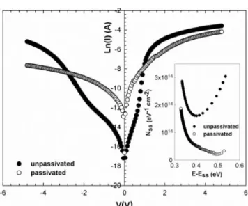
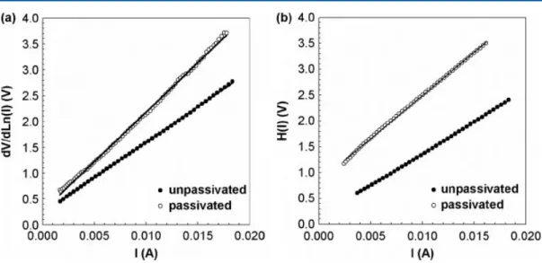
The effect of insulator layer thickness on the main electrical parameters in (Ni/Au)/AlxGa1-xN/AIN/GaN heterostructures
Tam metin
Şekil
Benzer Belgeler
Abdülmecit çağında, askeri ve mülki okulların yatılı öğrencileri, Hıdrellezlerde, buraya gelirler, koşup oynarlar, türlü eğlencelere dalıp çıkarak kuzu
In the third section, we investigate the thermal behavior of the back-to-back transducer in a finite closed circular baffle under high electrical drive and give some
This is because of the fact that the subquery in the ÔPRQ’ node can have a variable to be used by the subquery contained in the ÔTRQ’ node and in this case it is essential to
As an overall result, this study suggests that peer revision of students’ written texts provides a useful type of feedback as a complement to teacher feedback in second
Ibrahim, A., et al., Effects of annealing on copper substrate surface morphology and graphene growth by chemical vapor deposition. Jin, Y., et al., Roles of H2
Popularity and social features reflect social aspects of POIs in the search results: user count that indicates the number of users who have visited a POI, checkin count
We have shown, e.g., for (Zn,Mn)Se-based quantum wells, 36 that the microwave-induced heating of the Mn spin system, both resonant and nonresonant, can be experimentally
In this study, the optimal channel switching strategy is proposed for average capacity maximization under power constraints and considering a time delay for each channel
