IZ
MIR K
A
T
IP CE
L
E
BI UNIV
E
RSIT
Y
2
0
1
8
G
.
E
RSU
M.Sc. THESIS FEBRUARY 2018ENHANCEMENT OF THE ELECTRICAL PROPERTIES OF GRAPHENE FOR ELECTRONIC DEVICES
Thesis Advisor: Asst. Prof. Fethullah GUNES IZMIR KATIP CELEBI UNIVERSITY
GRADUATE SCHOOL OF NATURAL AND APPLIED SCIENCES
Department of Material Science and Engineering
Anabilim Dalı : Herhangi Mühendislik, Bilim Programı : Herhangi Program
FEBRUARY 2018
Thesis Advisor: Asst. Prof. Fethullah GUNES Department of Material Science and Engineering
Anabilim Dalı : Herhangi Mühendislik, Bilim Programı : Herhangi Program
M.Sc. THESIS Gulsum ERSU (Y130111028)
ENHANCEMENT OF THE ELECTRICAL PROPERTIES OF GRAPHENE FOR ELECTRONIC DEVICES
IZMIR KATIP CELEBI UNIVERSITY
ŞUBAT 2018
İZMİR KATİP ÇELEBİ ÜNİVERSİTESİ FEN BİLİMLERİ ENSTİTÜSÜ
ELEKTRONİK CİHAZLAR İÇİN GRAFENİN ELEKTRİKSEL ÖZELLİKLERİNİN GELİŞTİRİLMESİ
YÜKSEK LİSANS TEZİ Gülsüm ERSÜ
(Y130111028)
Malzeme Bilimi ve Mühendisliği Ana Bilim Dalı
Anabilim Dalı : Herhangi Mühendislik, Bilim Programı : Herhangi Program
v
Thesis Advisor :
Asst. Prof. Dr.Fethullah GUNES ... İzmir Katip Çelebi University
Jury Members :
Asst. Prof. Dr. Ahmet AYKAC ... İzmir Katip Çelebi University
Asst. Prof. Dr. Seckin ERDEN ... Ege University
Gulsum ERSU, a M.Sc. student of IKCU Graduate School Of Natural And Applied Sciences, successfully defended the thesis entitled “ENHANCEMENT OF THE ELECTRICAL PROPERTIES OF GRAPHENE FOR ELECTRONIC DEVICES ”, which she prepared after fulfilling the requirements specified in the associated legislations, before the jury whose signatures are below.
Date of Submission : 06.03.2018 Date of Defense : 06.02.2018
vii
ix FOREWORD
Firstly, I would like to thank my parents for their patience, support, and prayers during this time. I am especially grateful for their encouragement on whatever I decided to go for.
I would like to thank my advisor Asst. Prof. Fethullah Güneş for all his help, teaching and giving me an opportunity to do experimental research in his lab. I also would like to thank him for confidence me and giving me responsibility.
I would like to thank the committee members of my thesis for their participation.
Thanks to Asst. Prof. Ahmet Aykaç and Asst. Prof. Mustafa Erol for keeping their doors open when I needed help during my thesis completion process and for their helpful advice.
I am thankful to Dr. Caner Karakaya for his contributions.
v TABLE OF CONTENTS Page FOREWORD ... ix TABLE OF CONTENTS ... v ABBREVIATIONS ... vii SYMBOLS ... ix LIST OF TABLES ... xi
LIST OF FIGURES ... xiii
ABSTRACT ... xv
ÖZET ...xvii
INTRODUCTION ... 1
Graphene ... 1
Morphological Structure of Graphene ... 2
Electronic Structure of Graphene ... 3
Properties and Applications of Graphene ... 5
Graphene Production ... 6
1.5.1 Mechanical and chemical exfoliation ... 6
1.5.2 Epitaxial growth on silicon carbide ... 8
1.5.3 Chemical vapor deposition (CVD) ... 9
GROWTH AND CHARACTERIZATION OF GRAPHENE ... 11
Synthesis Flexible and Transparent Conductive Graphene Film ... 11
Materials and Methods ... 12
2.2.1 Pre-treatment of copper foil ... 12
2.2.2 Preparation of monolayer graphene film ... 13
2.2.3 Transfer process of graphene film ... 14
2.2.4 Characterization ... 15
Results and Discussion ... 16
2.3.1 Effect of pre-treatment process ... 16
2.3.2 Characterization of the CVD-graphene film ... 19
CONTROLLING THE ELECTRONIC PROPERTIES OF GRAPHENE ... 27
Electronic Modulation of Graphene via Doping Method ... 27
Materials and Methods ... 29
Characterization ... 30
Results and Discussion ... 30
vi
REFERENCES ... 39 CURRICULUM VITAE ... 47
vii ABBREVIATIONS 0D : Zero-dimensional 1D : One-dimensional 2D : Two-dimensional 3D : Three-dimensional CNT : Carbon nanotubes
OLED : Organic light-emitting diodes FET : Field-effect transistors
HOPG : Highly oriented pyrolytic graphite GO : Graphene oxide
rGO : Reduced graphene oxides SiC : Silicon Carbide
LED : Light emitting devices CVD : Chemical vapor deposition TCF : Transparent conductive film LCD : Liquid crystal display PMMA : Poly(methylmethacrylate)
APCVD : Atmospheric pressure chemical vapor deposition
CH4 : Methane
H2 : Hydrojen
Ar : Argon
PET : Polyethylene terephthalate CMP : Chemical-mechanical polish MFC : Mass flow controller
FeCl3 : Iron (III) chloride DI : Deionized water
N2 : Nitrogen
sccm : Standart cubic centimeters per minute IPA : Isopropyl alcohol
OM : Optical microscope AFM : Atomic force microscope
viii RMS : Root mean square
FWHM : Full-width half-minimum Rs : Sheet resistance
TCE :Transparent conductive electrode
T : Transmittance
HOMO : Highest occupied molecular level LUMO : Lowest unoccupied molecular level SAMs : Self-assembled monolayers
F-PBA : 4-Fluorophenyl boronic acid 2F-PBA : 3,4-Difluorophenyl boronic acid 3M-PBA : 3,4,5-Trimethoxyphenyl boronic acid BF3 : Boron trifluoride dimethyl etherate
TPA : 4,4''-bis(diphenylamino)-1,1':3',1''-terphenyl CAR : 4,4''-di-9H-carbazol-9-yl-1,1':3',1''-terphenyl DMF : N,N-Dimethylformamide
ix SYMBOLS 𝒗𝑭 : Fermi velocity 𝒌 ⃗⃗ : Wave vector ħ : Planck’s constant 𝝈𝑫𝑪 : Conductivity 𝝈𝑶𝑷 : Optical conductivity T : Transmittance Rs : Sheet resistance ρ : Resistivity t : Thickness σ : Conductivity q : Electron charge n : Carrier density µ : Mobility
xi LIST OF TABLES
Page Transmittance, sheet resistance, and σDC/σOP values for the layer-by-layer
graphene. ... 25 Table 3.1 : Electrical properties of graphene doped with various concentrations. ... 35
xiii LIST OF FIGURES
Page Allotropes of carbon namely Graphene, Fullerene, Carbon nanotube,
and Graphite [1]. ... 1
(a) Electronic configuration of sp2 hybridized (b) sp2 hybridized carbon and its orbital structure, (c) crystal structure of the graphene which contains two carbon atoms in a unit cell. ... 3
Electronic band structure of graphene [24]. ... 4
Procedure of mechanically exfoliated graphene and optical image of few layer graphene (dark purple contrast) and single-layer graphene (lighter purple contrast). Image cited from [58]. ... 7
Schematic representation of the graphene oxide synthesis by liquid-phase exfoliation (top-right) and reduction method (bottom-right). Reproduced from Ref.[59, 62]. ... 8
Schematic representation of epitaxial graphene growth on SiC. The blue broken line is the electrically ineffective buffer layer [71]. ... 9
Schematic representation of the CVD mechanisms of graphene growth on Cu foil. ... 10
(a) and (b) the digital image of chemical vapor deposition (CVD) system. (1) split tube furnace, (2) reaction chamber, (3) mass flow controller. ... 13
The time-dependent growth parameters used in this study and illustration of graphene growth process on Cu foil by CVD. ... 14
Transfer procedure of graphene film. ... 15
Images of characterization devices. ... 16
Schematic procedure of the sample preparation by CMP method. ... 17
(a) Digital images of Cu foils after the annealing and polishing treatment and optical images of (b) pristine, (c) pre-annealed and (d) polished Cu foils. Scale bars are 100 μm. ... 18
3D AFM topography image of the Cu surface (a) before and (b) after polishing, roughness mean square is abbreviated as RMS. ... 18
Optical images of graphene grown on (a) unpolished-Cu and (b) CMP-Cu. Graphene films were transfered on Si/SiO2. ... 19
Raman spectrum of transferred graphene films (a) grown at the different H2 flow rate, (b) plot of I2D/IG and ID/IG ratios as a function of H2 amount, (c) grown at the different CH4 flow, (d) corresponding I2D/IG and ID/IG. ... 21
xiv
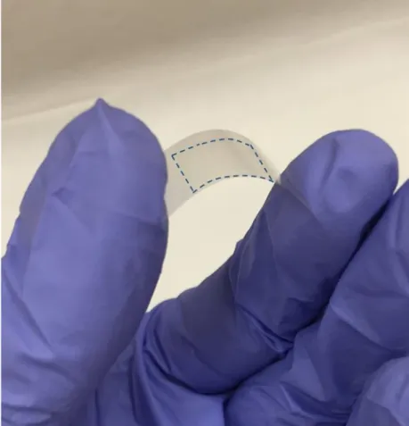
(a) Raman spectra of transferred graphene. The insert shows the Lorentzian fitting of 2D peak. The insert shows the 2D peak fitted by Lorentzian peaks. (b) Optical image of transferred graphene film. Arrows show incomplete adlayers (c) Raman mapping images of graphene for 2D peak as indicated from the image (b) with the dotted square (25 x 21 µm2). ... 22 Optical transmittance of graphene film transferred on PET substrate. 23 Photographs of of graphene films with from 1 layer to 4 layers on PET. ... 25 Figure 3.1 : (a) covalent, (b) non-covalent modification of graphene, (c) band structure of intrinsic, p-type and n-type graphene. ... 28 Figure 3.2 : Structure illustration of self-assembly monolayers (SAMs). ... 29 Figure 3.3 : SEM images of pristine graphene film. The white arrows indicate the wrinkles. ... 31 Figure 3.4 : Chemical strucrutes of SAMs. ... 31 Figure 3.5 : The raman spectrum obtained from pristine and modified graphene with different SAMs molecules a) the G (left) and 2D (right) bands (b) effect of doping on Raman G and 2D band position (c) intensity ratio. ... 33 Figure 3.6 : (a) Sheet carrier density, (b) mobility and conductivity of doped and undoped graphene. ... 34 Figure 4.1 : Photography of the graphene film. ... 38
xv
ENHANCEMENT OF THE ELECTRİCAL PROPERTİES OF GRAPHENE FOR ELECTRONİC DEVİCES
ABSTRACT
Graphene, a one-atom-thick two-dimensional material, has drawn great interest for many electronic and optoelectronic applications due to its extraordinary properties. The properties of the graphene can be modified with different chemical methods and introduced new properties, which widens its potential for applications. The non-covalent modification of graphene is one of the basic techniques for modifying the electrical properties of graphene without disrupting the structure.
In this thesis, the high-quality graphene has been synthesized and electrical properties of graphene have been tuned by using self-assembly monolayers (SAMs). For graphene synthesis, copper foil pre-treatment was performed using the mechanical-chemical polishing method. Afterwords, graphene films were synthesized on pre-cleaned copper foil by atmospheric pressure chemical vapor deposition under the optimized conditions. It was found that copper surface and growth conditions play a significant role in high quality graphene growth. Additionally, sheet resistance and mobility of graphene were measured by Hall Effect measurement system. The sheet resistance of graphene was found about 718 Ω/sq with 96.8% of transmittance. Furthermore, obtained graphene was doped with surface transfer method using various SAMs including 4-Fluorophenyl boronic acid, 3,4-Difluorophenyl boronic acid, 3,4,5-Trimethoxyphenyl boronic acid, Boron trifluoride dimethyl etherate, TPA and CAR. It has been found that SAMs modify the density of its charge carriers, thus, the electrical properties of graphene films have been altered. As a result, depending on the type of SAMs the carrier type of graphene can controllably be changed from p-type to n-type and the electrical properties of graphene could be modified by several SAMs. We believed that this study could open up a wide range of possibilities for electronic and optoelectronic applications.
xvii
ELEKTRONİK CİHAZLAR İÇİN GRAFENİN ELEKTRİKSEL ÖZELLİKLERİNİN GELİŞTİRİLMESİ
ÖZET
Bir atom kalınlığında iki boyutlu bir malzeme olan grafen, olağanüstü özelliklerinden dolayı elektronik ve optoelektronik uygulamalarda kullanılmak üzere büyük ilgi görmektedir. Bant boşluğu bulunmayan grafene yeni özellikler katmak yada varolan özelliklerini uygulamalar için istenilen seviyeye getirmek son zamanlarda çalışılan önemli bir konudur. Yüzey aktarımı yoluyla katkılama, kovalent olmayan bir bağ kurarak ve yapıyı bozmadan grafenin elektriksel özelliklerini değiştirmek için kullanılan temel yöntemlerden biridir.
Bu tez çalışmasında santimetre ölçekli, yüksek kalitede grafen filmler kimyasal buhar biriktirme yöntemi ile sentezlenmiş ve çeşitli tek katman olabilen moleküller kullanılarak elektriksel özellikleri değiştirilmiştir. Öncelikle, bakır folyo, mekanik-kimyasal parlatma yöntemi kullanılarak hazırlanmıştır. Daha sonra grafen, hazırlanan bu bakır folyolar üzerinde atmosferik basınçta kimyasal buhar biriktirme yöntemi kullanılarak sentezlenmiştir. Sentezlenen filmler analiz edilmek için farklı altlıklar üzerine transfer edilmiştir. Yapılan analiz çalışmaları sonucunda bakır yüzeyinin ve büyüme koşullarının grafenin büyümesinde önemli bir rol oynadığı belirlenmiştir. Ek olarak, grafenin levha direnci ve hareketliliği Hall Effect ölçüm cihazı kullanılarak ölçülmüştür. Sentezlenen grafenin levha direnci yaklaşık 718 Ω/sq ve optik geçirgenliği % 96.8 bulunmuştur. Daha sonra, yüzey transfer yöntemiyle grafen filmlere kendi kendine tek katman olabilen (SAM) molekülleri kullanılarak katkılama yapılmıştır. Kullanılan 4-Florofenil boronik asit, 3,4- Diflorofenil boronik asit, 3,4,5-Trimetoksifenil boronik asit, Bor trifluorür dietil eterat, TPA ve CAR SAM moleküllerinin grafenin yük taşıyıcılarının yoğunluğunu değiştirdiği ve dolayısıyla grafen filmlerin elektriksel özelliklerini değiştirdiği belirlenmiştir. Sonuç olarak, SAM moleküllerinin türüne bağlı olarak grafenin taşıyıcı türünün kontrollü olarak p-tipinden n-tipe dönüştürülebilir olduğu ve grafenin elektriksel özelliklerinin SAM ile modifiye edilebilir olduğu bulunmuştur. Sonuçlarımız, grafenin elektriksel özelliklerinin başarıyla değiştirildiğini ayrıca elektronik ve optoelektronik uygulamalar için uygun bir malzeme olarak kullanılabileceğini göstermektedir.
1 INTRODUCTION
Graphene
Graphene is a one-atom-thick two-dimensional (2D) sheets of hexagonal sp2 -hybridized carbon atoms. The honeycomb network of this unique material is a basic model of the three-dimensional (3D) graphite, one-dimensional (1D) carbon nanotubes (CNT) and zero-dimensional (0D) fullerenes, which are different types of carbon allotropes (Figure 1.1).
Allotropes of carbon namely Graphene, Fullerene, Carbon nanotube, and Graphite [1].
The first graphene was obtained by mechanical exfoliation of graphite in 2004. With this method, single and few-layer graphene flakes were formed which could be easily separated using a sticky tape [2]. It has been gaining appreciable attention from many research areas due to remarkable properties of such as electrical, mechanical, optical and thermal [3-5]. Graphene is the thinnest and also the strongest material ever
2
discovered, even though it is a single atom thick which makes it a highly transparent material absorbing only 2.3% of visible light [5-7]. This light-weight material has also other important features like high electron mobility, super-hydrophobicity, high elasticity and thermal conductivity [8-10]. Graphene can be classified as a semi-metal or zero-gap semiconductor of which the electrons behave as massless Dirac fermions [4, 11]. With these extraordinary properties, it has a high potential in many applications such as integrated circuits [12], sensors [13], transistors [14, 15], energy storage devices [16, 17], flexible and transparent electronic applications for solar cells and touch screens [18, 19].
Morphological Structure of Graphene
Graphene lattice, a 2D layers of carbon atoms packed in a honeycomb structure, is originated from the covalent bonding properties of carbon element in the group IV of the periodic table. Carbon element has 6 electrons and its electronic configuration denoted as 1s22s22p2, of which the four electrons are valence electrons. In such kind of electronic configuration carbon can be hybridized to form more stable compounds and results in different hybrid orbitals such as sp2 and sp3 hybridization. In sp2 hybridization, the s-orbital and two p-orbitals (2px, 2py), are situated in the second
energy level of carbon, creating three equivalent hybridized sp2 orbitals, and one 2p z
orbital remained unhybridized (Figure 1.2 a). Therefore, each carbon atom has three closest neighbours which bonded to the other three carbon atoms through the sp2
hybridized orbitals and constitutes short-strong covalent σ-bonds between adjacent atoms in the lattice of graphene. These strong molecular bonds keep graphene as a 2D-layer and also responsible for the mechanical strength (Figure 1.2 b). The remaining 2pz orbital which is unhybridized creates relatively long and diffusing
π-bonds with nearest carbon atoms and is perpendicular to the molecular plane. These bonds form electron cloud and responsible for controlling the interaction between different graphene layers. The lattice of the graphene in Figure 1.2 c shows that two sublattices, A and B, so the two atoms in each basic unit cell form the honeycomb lattice. The carbon-carbon bond distance is approximately 1.42Å and the two lattice vectors can be described as follows as [11, 20-22]:
3 𝑎1 = 𝑎
2 (3, √3), 𝑎2 = 𝑎
2 (3, −√3) (1.1)
(a) Electronic configuration of sp2 hybridized (b) sp2 hybridized carbon and its orbital structure, (c) crystal structure of the graphene which contains two carbon
atoms in a unit cell. Electronic Structure of Graphene
Graphene has unusual electronic properties due to its unique band structure. As have been discussed in the previous section, each carbon atom has a remaining one pz
electron, which is perpendicular to the planar structure, and they bind with one of the three closest carbon atoms, causing the formation of a half filled π bond.
4
In graphene unit cell, there are two atoms because of two different orientation of bonds. The energy dispersion of electrons are divided into two bands as bonding π-electrons (the lower energy valence band) and the anti-bonding π*-π-electrons (the higher energy conduction band) due to interaction among the atoms. Low-energy electronic band structure of graphene, which was described first by P.R. Wallace [23], is determined by these π and π* bands (Figure 1.3).
Electronic band structure of graphene [24].
The π and π* bands stay equal in energy because they are indistinctive at Fermi energy and also touch at six points in the Brillouin zone causing two conical K and K'. These points are called the Dirac or neutrality points and constitute excellent Dirac cones. Therefore graphene is generally referred as a semimetal or a zero gap semiconductor with a long-wavelength energy distribution. Charge carriers in graphene are identified by Dirac equation due to the linear dispersion of the bands:
𝐸 = ±𝒱Ϝℏ|𝑘⃗ | (1.2)
where the 𝒱Ϝ is the Fermi velocity (106 m/s) which is energy-independent and nearly 300 times smaller than the speed of light, 𝑘⃗ is the wave vector and ℏ is Planck’s constant [25-27]. From this equation, it is understood that the graphene has a linear distribution correlation, which is a characteristic of zero-mass particles as photons. Accordingly, the electrons act as massless Dirac fermions moving at the Fermi speed throughout the graphene lattice.
5 Properties and Applications of Graphene
The electrons have extra quantum confinement due to absence of the third dimension and this gives graphene various unique properties in many ways. One of the most extraordinary properties of the graphene is that electrons behave as massless particles or Dirac fermions. The carrier moves in the lattice with little scattering and so graphene sheets conduct electricity very well [2, 28, 29]. Since the graphene system possesses a zero band gap that let electrons to move easily without a need of energy input, it shows abnormal quantum hall effect and high mobility (>200,000 cm2/V.s). High field effect mobility and sensitivity to the field effect provide graphene to be used in ultra-high speed electronics as an alternative to carbon nanotube or silicon being used in modern technology [30, 31]. Furthermore, graphene is a very attractive material for mechanical reinforcement in composite applications due to mechanical strength (>1 TPa) of which ~200 times greater than steel. This makes graphene a high-quality composite material increasing the conductivity and strength of bulk materials along with their durability to heat and pressure [5, 32, 33]. Graphene-based composites could be used instead of materials used in many areas today such as medical implants, engineering materials for the aviation industry and renewable materials. Large specific surface area (~2630 m2g-1), ultra high loading capacity and
non-toxicity of graphene makes it a good candidate for drug delivery systems and biosensors [34]. Since graphene is highly sensitive to different gas molecules, it is possible to use it as a gas sensor for H2, O2 H2O, Cl2, CO, NO2, SO2, heavy metal
ions and vapor of volatile organic compounds [35-37]. Interactions between electrons and the graphene lattice makes it highly transparent, with an absorption of ∼2.3% for a visible light, flexible and strong. Accordingly, graphene has been examined in lithium-ion batteries, supercapacitors, solar cell, energy harvesting system, flexible and stretchable devices [38-40]. Graphene can be added to various battery devices, both as the anode or the cathode, so as to improve the performance of the system and enhance the charge/discharge cycle ratio [41]. The extreme variety of the physical and chemical properties of graphene has also been studied in flexible devices including photovoltaics, organic light-emitting diodes (OLEDs) and field-effect transistors (FETs) [42]. Graphene is used as a thermal interface material due to high thermal conductivity [43, 44].
6
The graphene's wavelength-independent absorption and high mobilities allow the application over a large spectral range from ultraviolet to infrared compared to the conventional semiconductor photodetectors. Schall et.al demonstrated 6″ wafer-scale graphene photodetector with a bandwidth larger than 76 GHz [45]. The compound of extraordinary properties of graphene opens the wide range of applications to overcome many restrictions of current materials in academic and industrial research.
Graphene Production
The current popularity of graphene in scientific research began in 2004 with A.K. Geim and K.S. Novoselov and his colleagues who reported for the first time that the graphene was synthesized using a simple adhesive tape [2, 8]. Although graphene was first theoretically investigated by Wallace in 1947, thin graphitic layers were experimentally synthesized on transition metal surfaces in the late 1970s [23] [46, 47]. In 1975, B. Lang et al.demonstrated structure of few-layer graphite using thermal decomposition methods however, it was not defined as graphene. [48, 49]. In 1999, Ruoff and co-workers attempted to produce graphitic flakes with mechanical exfoliation of HOPG (Highly Oriented Pyrolytic Graphite) but they did not report the electrical characterization of this material [50].
Graphene has a great attention for a while therefore many researchers have worked on different graphene synthesis methods for so long. In general, graphene has been produced or synthesized by two different approaches; top-down and bottom-up. The top-down approach is a breaking down of bulk graphitic materials into smaller ones (such as mechanical or chemical exfoliation and reduction methods). In the bottom-up approach, graphene is synthesized from atomic scale carbon-precursors through a set of chemical reactions (e.g. epitaxial growth and chemical vapor deposition) [51-53].
1.5.1 Mechanical and chemical exfoliation
After the discovery of graphene, the micromechanical cleavage method, top-down approach, have become the most commonly applied method. This method is based on separating different graphene layers from a bulk graphite. Graphite which is stacked layers of many graphene sheets has large lattice spacing in the perpendicular direction (3.35 Å) and a weak van der Waals force (2 eV/nm2) [54, 55]. Therefore
7
graphene can be produced from graphite by exfoliation using a simple sticky-tape and can be used in high-quality, defect-free graphene synthesis (Figure 1.4). This technique known as Scotch tape method generally used for research purposes because it is relatively inexpensive and offers 5 to 10 μm sized high-quality graphene films. On the other hand, glue residues can remain on the substrate and this method is not suitable for graphene synthesis in larger amounts. The quality of the graphene is very high in this technique nevertheless, the technique is not suitable for the mass-production. [56, 57]. This has motivated the search for alternative techniques for the large area graphene applications in the field of nanotechnology.
Procedure of mechanically exfoliated graphene and optical image of few layer graphene (dark purple contrast) and single-layer graphene (lighter purple
contrast). Image cited from [58].
Graphene can be produced by the different way of exfoliation (i.e. liquid-phase exfoliation, chemical reduction) in order to obtain a much higher amount of graphene (Figure 1.5). For example, sonication of graphite in water or in a solvent with almost the same surface energy as graphite leads to a stable suspension of graphene oxide (GO). The main idea behind this method is overcoming the van der Waals forces between the graphitic basal planes and reducing the energy barrier so that separating graphene layers from bulk graphite. The obtained GO layers can be chemically reduced to graphene sheets which known as reduced graphene oxides (rGO). Although, this method may be suitable for the mass production of graphene, the purity of produced rGOs is very low compared to pristine graphene and the number of defects is quite high, due to the oxidation and reduction procedures [59-61].
8
Schematic representation of the graphene oxide synthesis by liquid-phase exfoliation (top-right) and reduction method (bottom-right). Reproduced from
Ref.[59, 62]. 1.5.2 Epitaxial growth on silicon carbide
Although the mechanical exfoliation method is used to examine the properties of the graphene, it is necessary to obtain high-quality monolayer or few-layers graphene for electronic applications. Epitaxial growth of graphene surface is one of the most popular techniques for enlarging the size of graphene films [63]. The basic mechanism of epitaxial growth of graphene is shown in Figure 1.6 [64]. The epitaxial graphene refers to thermal graphitization of a silicon carbide (SiC) surface under high temperature (>1100 oC) and ultra-high vacuum. Under these conditions, silicon
atoms sublimate from SiC substrate due to the vapor pressure difference between silicon and carbon, resulting in carbon-rich surface transforming into an epitaxial layer of graphene at the surface [65-67]. Epitaxial graphene grown on SiC, has attracted the attention in electronic applications such as high-frequency electronics [30], FETs, light emitting devices (LED) [68] etc. With this method, the synthesized graphene does not need to be transferred to another substrate for device fabrication and thus it can be easily patterned. However, epitaxial graphene is restricted by the cost and size of the crystal substrates [69, 70].
9
Schematic representation of epitaxial graphene growth on SiC. The blue broken line is the electrically ineffective buffer layer [71].
1.5.3 Chemical vapor deposition (CVD)
For future applications, graphene synthesis is crucial to be in high-quality, large-sizes, easily obtainable and transferable to various substrates. Chemical vapor deposition (CVD) on polycrystalline transition metal catalysts such as Ni, Pd, Ru, or Cu is the most convenient method among all methods for graphene synthesis [72-74]. CVD methods include 3 steps: i) decomposition of carbon source, ii) adsorption, and iii) diffusion of molecules for the creation of a stable solid deposit on the catalyst. In the CVD process, high temperatures and a metal catalyst substrate are needed to provide the amount of energy required for breaking the carbon bonds (C-C = 347 kjmol-1, C=C = 614 kjmol-1, C≡C = 839 kjmol-1, C-H = 413 kjmol-1). Furthermore, the metal catalyst substrate should be annealed at high temperature for expanding its grain size [75]. During the synthesis an inert gas (argon or nitrogen), hydrogen and carbon source are used. Hydrogen is used for catalyzing the reaction between the metal catalyst and the carbon source, thus carbon atoms that result from the decomposition of carbon source are precipitated onto the metal substrate via surface absorption and then form graphene layers [76]. Following the reaction, the furnace is cooled down to reduce carbon solubility on the substrate and the carbon atoms diffused out so that the precipitated carbon atom is prevented from becoming bulk graphite [77]. In CVD method, copper (Cu) and nickel (Ni) are mostly used catalyst substrates, and the growth process shows similarity for both metals. The thickness and morphology of the graphene films can be controlled by the carbon solubility of the metal and growth conditions. Graphene films grown on Ni do not have a uniform single-layer graphene, mostly mixture of monolayer and few-layer, owing to the high solubility of carbon (>0.1 atomic%). However, Cu has low carbon solubility (<0.001 atomic%) due to a filled d-shells leading to a uniform monolayer graphene [78, 79]. Figure 1.7 shows a representation of the graphene growth on Cu by CVD.
10
The advantage of this method is to obtain high quality, continuous, large area graphene film and also possibility of transfering obtained graphene onto another substrate for device fabrication. Therefore, the CVD method for graphene synthesis was preferred in this thesis work.
Schematic representation of the CVD mechanisms of graphene growth on Cu foil.
11
GROWTH AND CHARACTERIZATION OF GRAPHENE
Synthesis Flexible and Transparent Conductive Graphene Film
Optical transparent flexible conductive films (TCFs) with high electrical conductivity has been greatly studied for use in many devices with electronic and optoelectronic property such as liquid crystal displays (LCDs), OLEDs, smart interactive displays, touchscreens. Such devices which become more common in our lives can protect their original properties after bending or stretching under some special environmental conditions [80, 81]. The materials that emerged in recent years such as 1D metallic nanowires, conductive polymers and carbon nanomaterials have been examined as alternative materials for producing flexible TCFs [82-84]. Among these alternative materials, conducting polymers are electrically unstable despite their desired properties such as electrical, optical and mechanical. Graphite and carbon nanotubes with high chemical stability, high transmittance, and high conductivity have been used for TCFs. However, the surface roughness and uniformity of these materials may lead to significant drawbacks and decrease the performances of the device. In contrast, graphene which is the 2D allotrope of carbon has been attracting a great deal of attention as a good candidate material due to high optical transmittance, flexibility and extraordinary electronic properties [85-88]. In addition, the synthesis of low-defect graphene is crucial to develop large-area graphene-based TCFs. As explained in chapter 1.5, CVD is the suitable method for large-area graphene synthesis. After graphene synthesis by CVD, graphene film must be isolated from the metal catalyst and transferred onto a requested transparent substrate for TCFs applications. Various techniques are used for transferring the CVD graphene, among them the wet chemical method is the most common approach [87, 89, 90]. In the standard chemical transfer procedure, graphene films should be protected from high stress. Generally, Poly(methylmethacrylate) (PMMA) is used as supporting layer owing to its low viscosity, flexibility, high transparency and good solubility in various organic solvents. After etching the metal substrate, free PMMA/graphene layer is transferred onto transparent dielectric substrate for the TCFs applications,
12
lastly, the PMMA layer is removed by dissolving in acetone [91, 92]. In this work, graphene was synthesized on prepared Cu foil by atmospheric pressure chemical vapor deposition (APCVD) process and successfully transferred. Graphene film on Cu was grown using methane gas (CH4) as a carbon source with the gas mixture of
argon (Ar) and hydrogen (H2). The amount of CH4/H2 gas mixture was optimized in
order to remove the amorphous carbon deposits and obtain highly crystalline, large area graphene. The growth time was also optimized to grow the layer of graphene and control of the layer thickness. The synthesized graphene film was successfully transferred onto polyethylene terephthalate (PET) substrate which is transparent and flexible. Additionally, the sheet resistance of graphene was examined according to the number of layers from 1 layer to 4 layers. The size of the synthesized graphene films depends on the dimensions of the Cu substrate and the size of the CVD chamber.
Materials and Methods
2.2.1 Pre-treatment of copper foil
Commercially available copper foil contains highly unwanted a native oxide (CuO, Cu2O), impurity and defect for graphene growth. The pre-treatment methods such as
electrochemical polishing and longtime thermal annealing are commonly used for removing native copper oxide layer and reducing the impurity or defect density on copper foils [93, 94].
In this study; pre-annealing and chemical-mechanical polishing (CMP) method were used for clean and flatten the copper foil surface. Protech split tube furnace was used for CVD method. A standard 2-inch quartz tube was used as the reaction chamber in a CVD furnace and a mass flow controller (MFC) was used to measure and control the flow rate of gases (Figure 2.1). Commercially available 80 µm thick copper foil (99.99% purity, 12 cm x 5 cm,) was placed onto a quartz sample holder and loaded into the center of a quartz tube within CVD furnace. The balancing of the entire CVD system was provided with a mixed gas flow of argon (Ar, 100 sccm) and hydrogen (H2, 200 sccm) and then the system was heated to 1075 ± 2 oC at a heating
ramp rate of 18 oC/min. After the system reached to 1075 oC, the Cu foil was pre-annealed for 2h under ambient pressure in order to enlarge the size of Cu grain and then the system was let to cool down to the room temperature with the same flow
13
ratio of Ar/H2. Finally, pre-annealed Cu foil was chemical-mechanical polished with
Iron(III) chloride (FeCl3) solution using laboratory tissue to obtain a flat surface. In
this method, the Cu surface was wet with diluted FeCl3 and tissue was moved all
over the surface by applying circular motion and equal pressure. After CMP, the copper foil completely rinsed using deionized (DI) water and then dried by a nitrogen (N2) flow for 2 min.
(a) and (b) the digital image of chemical vapor deposition (CVD) system. (1) split tube furnace, (2) reaction chamber, (3) mass flow controller.
2.2.2 Preparation of monolayer graphene film
Graphene layers were synthesized on pre-treated Cu foil by APCVD. Figure 2.2 shows the graphene growth process. The prepared Cu foil substrate was put onto quartz sample holder and loaded into hot center of quartz tube furnace. Then, the temperature was increased up to 1075 ± 2 °C with 1000 sccm (standard cubic centimeters per minute) of Ar gas and 80 sccm of H2 gas. The Cu foil was annealed
for 40 min at this temperature prior to growth to enlarge the grain size and to provide a smooth surface. Subsequently, 12 sccm of CH4 gas that used as a carbon source
was released into the CVD system for 1 min at the same temperature to grow the graphene layer on Cu foil. After growth, the CH4 was turned off and the chamber
14
The time-dependent growth parameters used in this study and illustration of graphene growth process on Cu foil by CVD.
2.2.3 Transfer process of graphene film
Graphene grown by CVD has to be transferred from the metal substrate to the target substrates for most practical applications. In this study, the graphene was transferred onto different substrate since a copper foil is not suitable to use as a substrate in the electrical, physical and chemical measurements. Graphene films were transferred using the PMMA (in 4% chlorobenzene, 950,000 molecular weight) based technique. After synthesis, the prepared polymethyl methacrylate solution (PMMA, 20 mg/mL) was coated by spin-coater at 2000 rpm for 1 min on the graphene/copper foils as a
15
supporting layer and dried in air. In order to etch the copper foil, the graphene/PMMA films were floated on the surface of the copper etchant solution (FeCl3, Transene CE100) for 1 h. The PMMA/graphene suspended films were
washed by DI water (3 times of 20 min each) to clean the substrate from any residual copper etchant. The target substrate (Si/SiO2 or PET) was sonicated during 10 min in
acetone, isopropyl alcohol (IPA) and DI water respectively and dried using a nitrogen gun. After this procedure, the graphene sheets with PMMA were transferred onto a target substrate (Si/SiO2 or PET) and dried at 70 oC for 20 min using drying
oven so as to decrease the amount of water and also to improve the contact between PMMA/graphene/wafer. Finally, the PMMA layer was dissolved in hot acetone during 5 min and then immersed in IPA and ethanol, respectively, at room temperature. The graphene/wafer samples were dried using a nitrogen gun (Figure 2.3).
Transfer procedure of graphene film. 2.2.4 Characterization
The optical microscopy (Nicon Eclipse) and atomic force microscopy (Nanosurf, easyscan 2) were used for characterizing the morphology of the Cu foils. Optical characterization of graphene was performed by confocal Raman spectroscopy
16
(Renishaw) with 532 nm laser wavelength at room temperature and 100x objective, ultraviolet-visible (uv-vis) spectroscopy (Thermo Scientific, Evolution Array) and optical microscopy. Hall effect measurement system ( Ecopia, HMS-3000) was used for electrical characterization of graphene at room temperature (Figure 2.4).
Images of characterization devices. Results and Discussion
2.3.1 Effect of pre-treatment process
In the CVD growth, reducing the graphene nucleation density is of great importance for obtaining large area graphene domains since the nucleation density is highly related to active sites on copper for graphene nucleation. The defects of as-received commercial copper foil surface such as roughness, grain boundary, surface irregularities serve as nucleation seeds of graphene domains [95-97]. The formation of nucleation seeds could be reduced by CMP process and thus graphene could only nucleate on the flat Cu surface instead of Cu defects where the nucleation seeds are especially high. Figure 2.5 shows an illustration of the copper pre-cleaning by CMP method.
17
Schematic procedure of the sample preparation by CMP method. Considering the significance of the Cu foil characteristics on graphene synthesis, the surface morphology and roughness of commercially available foils were investigated using the optical microscopy (OM), and atomic force microscopy (AFM). Figure 2.6 (a) shows photographs of the pristine, pre-annealed and polished Cu foils respectively. The color of the Cu foils has remarkably changed owing to the reduction of the oxidized layer and the recrystallization of the Cu surface. The surface morphology of the pristine foils shows the striation lines and the rough surface that occur during the rolling process used for the manufacture of the Cu sheets. In addition, some defect such as surface pits and impurity particles can be observed which may act as nucleation sites. After pre-annealing at 1075°C, the morphologies were mostly reformed and grain boundaries became more pronounced while the structural defect lines are reduced (Figure 2.6 b and c). The pre-annealed Cu foil was polished using acid treatment to achieve a more uniform surface. Figure 2.6 (d) shows that polished Cu has a sufficiently smoother surface than that of the reference samples. It was observed that the indentation was decreased and impurities were mostly disappeared after polishing.
18
(a) Digital images of Cu foils after the annealing and polishing treatment and optical images of (b) pristine, (c) pre-annealed and (d) polished Cu
foils. Scale bars are 100 μm.
The surface roughness of Cu foils was characterized by AFM. Figure 2.7 shows the surface topology and root mean square (RMS) roughness measurement data of foils applied to Gaussian filtering to suppress the waviness effect and scanned at various points in a 10x10 µm area. It is seen that after polishing, the roughness of the Cu surface is reduced from 167 nm to 81nm and Cu surface became smoother.
3D AFM topography image of the Cu surface (a) before and (b) after polishing, roughness mean square is abbreviated as RMS.
19
These results are consistent with optical microscopy results and with earlier reports indicating that annealing and polishing of Cu reduce surface contamination and help to obtain a flat surface [98-101]. However, CMP method for the preparing metal substrate before graphene growth is rarely reported. Our procedure is a simple method to polish the Cu foils, of which surface roughness was decreased to 81nm. To demonstrate the effect of Cu foil on graphene quality, graphene film was synthesized on unpolished and CMP copper foils and transferred onto Si/SiO2
substrate. The optical microscopy results of graphene grown on polished (CMP-Cu) and unpolished Cu foils were compared in Figure 2.8. The graphene which was grown on unpolished Cu was nucleated randomly and contained incomplete areas due to the existence of impurity particles (Figure 2.8 a). In contrast, graphene film grown on CMP-Cu was highly continuous (Figure 2.8 b). These images prove that pre-treatment process of Cu foil is very effective to synthesize high quality and continuous graphene.
Optical images of graphene grown on (a) unpolished-Cu and (b) CMP-Cu. Graphene films were transfered on Si/SiO2.
2.3.2 Characterization of the CVD-graphene film
The APCVD process has been optimized by adjusting the CH4/H2 flow rate to
synthesize a single-layer graphene. Quality of the CVD grown graphene is greatly dependent on the hydrogen contribution, therefore it is widely used for the graphene growth processes. Hydrogen gas is mainly used for activating the creation of surface-bound carbon and also for the removal of amorphous carbon impurities, so that the number of layers, cyristallinity, and morphology of the graphene domains can be controlled [95, 102, 103]. In this study, the H2 amount in the CH4/H2 gas mixture was
20
optimized in order to reduce defect density and also to grow large area, monolayer graphene. The flow rate (1000 sccm) of Ar during the entire process and CH4 (20
sccm) for the growth process and also growth time were constant. Effect of different flow rates of H2 on graphene growth were investigated using Raman spectroscopy as
shown in Figure 2.9. Raman spectroscopy can inform about crystal size, the existence of sp2-sp3 hybridization, number of graphene layers, defects and disorder. Raman spectra show D, G and 2D (or G') common bands, appearing at about 1350 cm-1, 1582 cm-1 and 2700 cm-1 respectively, for graphitic materials. The D band, at about half of the frequency of the 2D band, is associated with sp3-hybridized carbon and this means defect or disorder for graphene. The G band is common to all sp2 carbon systems, occurs from stretching of the C-C bond. The 2D band is the second most prominent peak that observed because of two-phonon lattice resonant process. The ID/IG ratio (intensity of the D peak to that of the G peak) measured from
the Raman spectrum is used to determine disorder degree in graphitic materials. The increment in the ID/IG ratio refers to the decrement of the number of graphite
microcrystallites. Furthermore, I2D/IG ratio is used to determine the number of
graphene layers [104-107]. As can be observed from Figure 2.9 (b), if the concentration of hydrogen is increased the defect peak intensity in the Raman spectrum decreases from 1.6 to 0.5 whereas the I2D/IG ratio increases. The I2D / IG
density ratio of the graphene which was synthesized with 80 sccm flow rate of H2
was found as approximately 1.89 and this result seems to be useful for improving the graphene quality in our process conditions. Moreover, the ratio of CH4 was varied
from 10% to 25% in present growth parameters to examine the effect of methane partial pressure on raman quality (Figure 2.9 c,d). Graphene films synthesized at the high CH4 flow rate (>12 sccm) have much weaker 2D peaks and large structural
defects (high ID/IG ratio values) likewise very low CH4 flow rate (8 sccm and 10
sccm). However, as CH4 was increased up to 12 sccm, the I2D/IG ratio was increased
showing the monolayer graphene was obtained [104]. Consistent results were obtained with the results obtained by other research groups [103, 108-111].
21
Raman spectrum of transferred graphene films (a) grown at the different H2 flow rate, (b) plot of I2D/IG and ID/IG ratios as a function of H2 amount,
(c) grown at the different CH4 flow, (d) corresponding I2D/IG and ID/IG.
According to the obtained results, 12/80 sccm ratio of CH4/ H2 was chosen as the
best ratio obtained in this work, which is close to that of monolayer graphene, and this ratio was used in the following experiments. On the basis of this results further optimization steps were made and the growth time was decreased. Using the optimal conditions graphene films were synthesized at 1075 oC with 1000/80/12 sccm flow
rate of Ar/H2/CH4 for a 1 min on Cu foil by APCVD. The prepared graphene films
were transferred onto Si/SiO2 (p-doped silicon with about 300 nm oxide) and PET
substrate for electrical and optical characterizations. The Raman spectra were measured from monolayer region and the peak position of D, G and 2D appear around 1347 cm-1, 1586 cm-1. 2680 cm-1, respectively (Figure 2.10 a). Morever, ID/IG
and I2D/IG were found about 0,3 and 3, respectively, and the insert figure shows a
strong and narrow 2D peak with a full-width half-maximum (FWHM) of 35 cm-1. This symmetric 2D peak can be well fitted by a single Lorentzian curve. These results verify the presence of a single-layer graphene with a low structural disorder and also the number of layers were confirmed using ωG(n) = 1581.6 + 11/(1 + n 1.6)
22
microscope images shown in Figure 2.10 (b) indicate that the graphene film is mostly homogeneous and continuous and have a small amount of dark region (dotted circle) which are identified as the bilayer or multilayer graphene [114]. Moreover, 2D bands were taken over a 25 x 21 µm2 area with a 0.5 µm step size to further investigate the
quality, uniformity and thickness of graphene, as shown in Figure 2.10 (c). From the optical contrast it appears that the 2D band is generally uniform over the examined region, indicating that the prepared high-quality graphene is suitable for transparent electrode application [115].
(a) Raman spectra of transferred graphene. The insert shows the Lorentzian fitting of 2D peak. The insert shows the 2D peak fitted by Lorentzian
peaks. (b) Optical image of transferred graphene film. Arrows show incomplete adlayers (c) Raman mapping images of graphene for 2D peak as indicated from the
image (b) with the dotted square (25 x 21 µm2).
For transparent conductive film applications, the optical and electrical properties of 1.5 x 1.5 cm2 graphene films were measured by UV-visible spectrometer and Hall effect measurement system respectively. The sheet resistance (Rs) is very important
factor for conductive films and determine their performance. In order to measure sheet resistance, graphene films were transferred onto Si/SiO2 wafer and then four
indium electrodes were connected on each corner of the film square that making ohmic contact. Finally, the measurements of sheet resistance and mobility of graphene were found about 718 Ω/sq and 1000 cm2/V.s, respectively, with a carrier density of 1012 cm-2. The mobility mostly depends on grain boundaries, dislocations, residue from the transfer processing and other surface properties. Therefore, the
23
mobility of CVD-graphene shows lower mobility values, from less than 1000 cm2/V.s up to 10000 cm2/V.s [116, 117].
Additionally, the graphene films were transferred onto a PET substrate to determine the availability of high-quality, monolayer graphene in large areas. The transmittance of graphene film was measured by UV-Vis spectroscopy using a piece of PET as baseline. The average value of transmittance of 96.8% at λ =550 nm was observed (Figure 2.11). These results are slightly lower than the theoretical value (97.7%) which might be due to the polymer residue or other impurities [7, 118]. It has been determined that graphene films synthesized in this study show a homogeneous optical transmittance being suitable for transparent conductive electrode (TCE) applications.
Optical transmittance of graphene film transferred on PET substrate.
The high value of transmittance (T) and conductivity (with low sheet resistance) are always desired for TCE applications. Nevertheless, sheet resistance and transmittance are inversely related as can be understood from the equation 2.1.
𝜎𝐷𝐶 𝜎𝑂𝑃 =
188.5
24
In the equation, σDC is conductivity, σOP is optical conductivity, Rs is sheet resistance,
and T is transmittance [119]. Using this equation, electrical to optical conductivity ratio was found approximately 16. The σDC/σOP ratio is important to enhance the
performance of TCE. Accordingly, a layer-by-layer approach used in previous reports
was utilized to alter the conductivity ratio [75, 87, 120]. Multilayer “graphene stacks” were prepared by repeating transfer process on the same PET substrate. The prepared films are shown in Figure 2.12. The measured transmittance and sheet resistance value and the calculated σDC/σOP values for layer-by-layer graphene are
given in Table 2.1. It has been observed that the transmittance of graphene film was reduced by about 3% by addition of each graphene layer, which is consistent with the previously reported values for the absorption of light (~2.3%) for each graphene layer [7]. Furthermore, the sheet resistance decreases as the number of layers increases. Because the layer-by-layer process provides extra ways to move the electrons and holes in the film. The obtained ratio of σDC/σop value for 1 layer
graphene is better than that of the reported value (0.7 – 11), yet it is still not at the desired value (>35) in TCE industry standards [121].
25
Photographs of of graphene films with from 1 layer to 4 layers on PET.
Transmittance, sheet resistance, and σDC/σOP values for the layer-by-layer
graphene.
1-layer 2-layers 3-layers 4-layers
Transmittance(%) ~97 ~94 ~91 ~88
Sheet Resistance (Ω/sq) 718 538 306 226
27
CONTROLLING THE ELECTRONIC PROPERTIES OF GRAPHENE
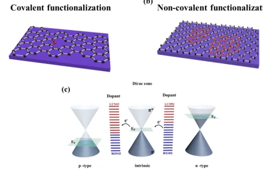
Electronic Modulation of Graphene via Doping Method
Graphene, a gapless material, is one of the most attractive materials for flexible and transparent electronic applications due to its unusual electronic properties. However, the potential use of the graphene in some applications is limited due to the zero band gap and therefore altering the band gap and Fermi level (or workfunction) of graphene is a critical issue. There are many approaches to modify the electronic properties of the graphene by shifting the Fermi level, the most common of which is the chemical modification or doping process. These approaches can be categorized as covalent, with the chemisorption on basal plane, and noncovalent, with physisorption on the surface. The covalent modification also known as substitutional doping refers to the addition of heteroatoms which are electron donors or acceptors in the graphene lattice. These heteroatoms covalently bond with carbon atoms in the graphene lattice and transform sp2 hybridization of carbon to sp3 via breaking the C-C π- and σ-bonds, as shown in Figure 3.1(a). Thus, the geometric and electronic band structure of graphene is modified, which creates a band gap and causes p- and n-type conductivity. The non-covalent modification also known as surface transfer doping occurs by electron exchange between dopant, which adsorbs on the surface through weak van der Waals interaction, and graphene lattice. Such modification generally is achieved by spin-coating or dip coating of a dopant solution changing the electronic properties without disrupting the structure of graphene (Figure 3.1b) [122-126]. Figure 3.1(c) shows the Fermi energy levels (EF) and band structures of intrinsic, p-
and n-type graphene. The linear valence band (π) and conduction bands (π*) touch each other in the Dirac points and these π electrons (electrons and holes) having opposite charge are used to form noncovalent bonding in the surface transfer doping. Charge transfer is related to the difference between the Fermi level of graphene and the highest occupied molecular level (HOMO) or the lowest unoccupied molecular level (LUMO) of the dopant. If the LUMO of dopant is below the Fermi level of graphene, the dopant act as an acceptor and charge (holes) passes through to the
28
dopant from the graphene, hence Fermi level of graphene downshifts and becomes p-type. If the HOMO of dopant is over the Fermi level of graphene, the dopant act as a donor and charge (electrons) transfers from dopant to the graphene so that Fermi level of graphene upshifts and becomes n-type [127-129]. By using this method, the charge carrier concentration and the work function of graphene can be controlled.
Figure 3.1 : (a) covalent, (b) non-covalent modification of graphene, (c) band structure of intrinsic, p-type and n-type graphene.
Many different chemical substances have been studied for the functionalization of graphene, and self-assembled monolayers (SAMs) are one of them. SAMs are well-oriented, stable and ultrathin layers ( ~ 1-3 nm) that uniformly bond with the surface through chemical or physical interactions between molecules and substrate. SAMs are prefered in organic electronic and nanotechnological applications due to their flexibility, low-cost and comparably easy fabrication process. The molecular structure of SAMs which is illustrated in Figure 3.2 consists of three main groups: (i) surface-active head group, binding with the substrate by a strong or a weak bond, (ii) tail, having aromatic structure and determining the thickness of SAMs, (iii) functional end groups, identifying the surface properties of SAMs [130].
29
Figure 3.2 : Structure illustration of self-assembly monolayers (SAMs). SAMs have been recently used to produce n- and p-type graphene by controlling charge carrier of graphene [131-134]. Park et al have reported the modification of electronic properties of graphene using SAMs with electron donor or acceptor functional groups openinig its band gap [135].
In this study, the effect of various SAMs on the electronic properties of CVD-grown graphene film was investigated. The charge carrier density and conductivity of graphene were studied as a function of dopant type and molarity.
Materials and Methods
4-Fluorophenyl boronic acid (F-PBA), 3,4-Difluorophenyl boronic acid (2F-PBA), 3,4,5-Trimethoxyphenyl boronic acid (3M-PBA), Boron trifluoride dimethyl etherate (BF3), 4,4''-bis(diphenylamino)-1,1':3',1''-terphenyl (TPA) and 4,4''-di-9H-carbazol-9-yl-1,1':3',1''-terphenyl (CAR) with carboxylic acid were used as SAMs to modify electrical properties of graphene. Each of these molecules were prepared 10-4 M concentration at room temperature. F-PBA, 2F-PBA, 3M-PBA were dissolved in N,N-Dimethylformamide (DMF, Sıgma-Aldrıch, D158550), BF3 was dissolved in methanol (Merck, 1060092511), TPA and CAR were dissolved in dimethyl sulfoxide (DMSO).
Graphene samples which were synthesized and transferred as described in chapter 2 were kept in the prepared SAMs solution for 24 hours and then rinsed to remove residues and finally dried using nitrogen gun.
30 Characterization
Scanning electron microscopy (ZEISS, GeminiSEM Sigma 300VP) was used for surface characterization of pristine and doped graphene. The optical characteristic and quality of samples were analyzed using Renishaw inVia Raman Spectroscopy with 532 nm laser wavelength and UV-vis spectroscopy (Thermo Scientific, Evolution Array). The electrical characterization of graphene was measured at room temperature using Hall effect measurement system (Ecopia, HMS-3000).
Results and Discussion
The surface morphology of synthesized graphene film is shown in Figure 3.3. Some white lines were observed on the graphene film, which are wrinkles forming during the transfer due to the differences in thermal expansion coefficients of the graphene and the Cu-foil (αgraphene = –6 × 10⁻⁶/K at 27 °C; αCu = 24 × 10-6/K ) [136-138]. These
wrinkles prove the continuity of the grown graphene.
Changing the electronic properties of graphene having a zero band gap is crucial for use in future electronic applications. For this purpose, after graphene films were synthesized and transferred onto Si/SiO2 substrate as mentioned in the previous
section, chemical doping treatments were performed by dipping in chemicals for 24h at room temperature. The chemical structures of various SAMs used for tuning electronic properties of graphene are shown in Figure 3.4.
31
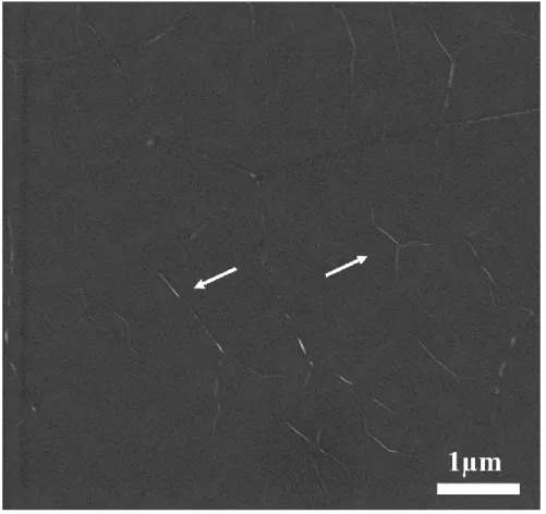
Figure 3.3 : SEM images of pristine graphene film. The white arrows indicate the wrinkles.
32
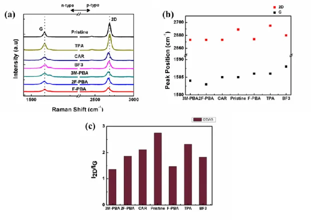
Raman spectroscopy is a useful method to examine the doping behavior of graphene by analysing the G and 2D bands position. The characteristic G and 2D bands alter depending on the doping effect. The Raman 2D and G band peaks positions are blueshifted (upshift) with electron-withdrawing dopant and redshifted (downshift) with electron donating dopant. As shown in Figure 3.5, the difference in the G and 2D peak positions indicate the alteration of the graphene electronic state. The up-shifting of G band indicates that charge transfer from graphene to dopant while the down-shifting indicates that charge transfer from dopant to graphene. Depending on doping type, Raman intensity as well as G and 2D peak positions are changing. It is seen in Figure 3.5(c) that intensity ratio (I2D/IG) was remarkably decreased after
doping because of all molecules used have large aromatic-ring structures. This aromatic-ring, having either electron-donor or electron-acceptor groups, enables the molecule binding to the surface of graphene by π–π interaction and results in intensity decrease [139, 140]. These results indicating changes in peak positions and intensities are evidenced that the graphene was effectively doped by SAMs. Although F-PBA and 2F-PBA are acceptor molecules, downshifting G and 2D band demonstrated that these molecules act as a donor and make n-type graphene. This result is believed to be due to the absence of an σ* OH orbital of which is an electron acceptor, or to the loss of hydrogen bond donor ability of the hydroxyl groups [141, 142].
33
Figure 3.5 : The raman spectrum obtained from pristine and modified graphene with different SAMs molecules a) the G (left) and 2D (right) bands (b) effect of doping on
Raman G and 2D band position (c) intensity ratio.
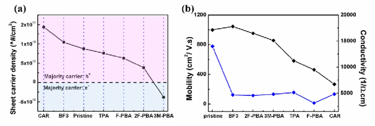
To further demonstrate the doping effects and examine the effect on the electronic properties of graphene, Hall measurement technique was used. Transferred graphene samples (1.5 cm x 1.5 cm) onto Si/SiO2 were doped with SAMs for 24h by dipping
method and the sheet carrier density and mobility measurements were performed at 300 K. Hall effect measurement results for these graphene films are shown in Figure 3.6. The carrier density of undoped graphene was measured about 8.7 x 1012 cm-2 with an average mobility of 1000 cm2/V.s, which is similar to previously observed results [143, 144]. The lower mobility than kish graphene is caused by the defects formed during transfer process or due to the bilayer graphene regions. The sheet carrier density was increased with BF3 and CAR doping and achieved to 1.4 x 1013 cm-2 whereas, it was decreased with TPA, F-PBA and 2F-PBA dopings
and reached about to 3.8 1012 cm-2. When graphene doped with 3M-PBA, the carrier type changed from p-type to n-type and carrier density was measured as about 3.85 1012 cm-2. The reducing in mobility after doping indicates that the graphene becomes n-type. Because of electron-donor nature of 3M-PBA, the conductivity of graphene decreased so that the sheet resistance increased and graphene became n-type [145].
34
The relation between sheet resistance (Rs), conductivity (σ) and mobility (µ) are
described as: 𝑅𝑠 = 𝜌 𝑡 𝑎𝑛𝑑 𝜌 = 1 𝜎= 1 𝑞𝑛𝜇 (3.1)
where ρ is the resistivity, t is the film thickness, q is electron charge (1.6 x10⁻¹⁹ C),
and n is the carrier density [121]. In the case of other dopants, the charge transfer activity between graphene and dopants were reduced. This may be due to the fact that large doping groups inhibit carrier movement [146].
Figure 3.6 : (a) Sheet carrier density, (b) mobility and conductivity of doped and undoped graphene.
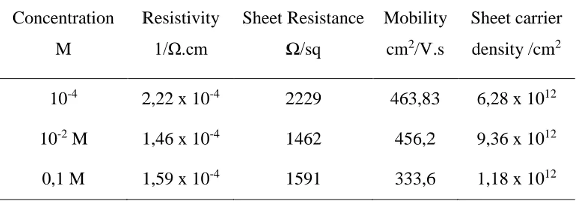
The ability to alter the electrical properties of the graphene to the desired level is very important for device applications. Therefore, various concentrations of F-PBA SAM solution in DMF were prepared and graphene films with 1.5 x 1.5 cm2 size were doped for 1h. The mobility and carrier concentration of graphene doped with different concentration were compared in Table 3.1. It was observed that the properties of CVD-grown graphene could be controlled through changing the concentration of SAMs applied. It has been determined that very low concentration (0.0001 M) solution of F-PBA has a stronger doping effect than that of high concentration solution (0.1 M). The mobility was found about 464 cm2/V.s and 334
35
Table 3.1 : Electrical properties of graphene doped with various concentrations. Concentration M Resistivity 1/Ω.cm Sheet Resistance Ω/sq Mobility cm2/V.s Sheet carrier density /cm2 10-4 2,22 x 10⁻⁴ 2229 463,83 6,28 x 10¹² 10-2 M 1,46 x 10⁻⁴ 1462 456,2 9,36 x 10¹² 0,1 M 1,59 x 10⁻⁴ 1591 333,6 1,18 x 10¹²
![Figure 3.2 : Structure illustration of self-assembly monolayers (SAMs). SAMs have been recently used to produce n- and p-type graphene by controlling charge carrier of graphene [131-134]](https://thumb-eu.123doks.com/thumbv2/9libnet/3708354.24896/55.892.263.697.138.352/structure-illustration-assembly-monolayers-recently-graphene-controlling-graphene.webp)