Electronic and optical properties of stanane and armchair stanane
nanoribbons
Mojde Fadaie1,2 · Daryoosh Dideban3 · Og̈uz Gülseren4
Received: 13 October 2019 / Accepted: 24 April 2020 / Published online: 26 May 2020 © Springer-Verlag GmbH Germany, part of Springer Nature 2020
Abstract
In this study, we performed a density functional theory based investigation of the structural, electronic, and optical properties of a stanane, fully hydrogenated stanene SnH, and armchair stanane nanoribbons ASnHNRs. Our full geometry optimization calculations show stanane has 0.84 Å buckled height and the buckled structure is preserved in ASnHNRs. The optimized lattice parameter of stanane, Sn–Sn, and Sn–H bond length are 4.58 Å, 2.75Å, and 1.73 Å, respectively. Electronic structure calculations show that stanane is a moderate-band-gap semiconductor with a direct band gap of 1.2 eV and ASnHNRs are wide-band-gap semiconductors. The band gap of ASnHNRs decreases as the ribbons width increases. We investigated the optical properties for two directions of polarization. For perpendicular-polarized light, the imaginary part of dielectric func-tion 𝜀2(𝜔) of stanane peaks between 5 and 10 eV; while for the parallel-polarized light, the peaks are seen in a wide range of energy. According to the results, stanane is a good absorptive matter, especially for visible regions of the electromagnetic spectrum. The presence of anisotropy with respect to the type of light polarization is observed in ASnHNRs also. In these structures, the main peak of 𝜀2(𝜔) is located at 3.4 eV for parallel- and in 6–8 eV for perpendicular-polarized light.
Keywords Stanene · Two-dimensional structure · Dielectric function · Structural properties · Optical properties · Stanane · Topological insulator
1 Introduction
Graphene is a two-dimensional honeycomb lattice of carbon atoms which has attracted a great deal of atten-tion because of its unique mechanical, magnetic, and electronic properties [1–3]. Theoretical and experimen-tal investigations have shown that graphene can exist in quasi-one-dimensional structures [4–6] which are called graphene nanoribbons (GNRs). The electronic properties of these materials are closely related to their dimension-ality. In contrast to graphene, GNRs are nonzero band
gap structures [7]. Various theoretical and experimental studies show the remarkable properties of GNRs. Some of these investigations focus on the adsorption of single atoms and molecules on the bare graphene and graphene nanoribbons [8–11]. These new structures could be suit-able candidates for use in nano-scale electronics [12], bio-electronics [13], gas sensors [14], hydrogen storage [15], and spintronic devices [16]. Among various additive atoms and molecules, hydrogen has attracted special attention. By adding hydrogen, zero-gap semiconductor graphene changes into the wide-gap semiconductor graphane [17]. Studies show that graphane nanoribbons exhibit more favorable formation energies than experimentally avail-able graphene nanoribbons [18]. The properties of gra-phene motivated scientists to investigate other elements in the fourth column of the periodic table. First, silicene and germanene, which are 2D structures of silicon and germanium, were fabricated in the laboratory [19, 20] after that tin atoms were considered [21]. The 2D struc-ture of tin atoms, which is called stanene, exhibits notable properties [22–24]. Similar to graphene, these structures have high carrier mobilities [25]. However, their zero or
* Mojde Fadaie
[email protected]; [email protected]
1 Department of Physics, Koç University, Istanbul, Turkey 2 Department of Physics, University of Montreal - MIL
Campus, Montreal, Canada
3 Department of Electrical and Computer Engineering,
University of Kashan, Kashan, Iran
very small gap limits their use, especially in electronic applications. Recently, fully hydrogenated germanene has been fabricated in the laboratory [26]. Germanane is a semiconductor with a moderate band gap. This moder-ate band gap brings new opportunities for applications of fourth-group 2D structures. It is worth noting that the dynamic stability for the stanene nanoribbon under study was investigated by calculating the phonon spectra as pre-sented in the literature [27]. None of them showed imagi-nary frequencies, indicating that they are all dynamically stable. On the other hand, the dynamic stability of nanor-ibbons comprised of stanene and other group IV materials are comprehensively investigated and proven in the recent works [28, 29]. In this work, we perform a density func-tional theory (DFT) study of fully hydrogenated stanene and also armchair stanane nanoribbons (ASnHNRs). We initially give a brief description of the computational method and the relevant parameters which were used in our calculations. Then, the structural properties of both stanane and ASnHNRs are investigated. After that, their electronic properties are discussed in detail. Finally, we analyze our calculations for the optical properties.
2 Methods
All of the calculations in this work are implemented using the Siesta code which is based on the density functional theory (DFT). We adopted the Perdew–Burke–Ernzerhof (PBE) [30] exchange-correlation functional of the gen-eralized gradient approximation (GGA) and 70 Ry cutoff energy in all computations. We started with 2D stanane which is derived from the hydrogenation of stanene, and then the armchair nanoribbons. The sampling for Brillouin zone integration was performed using the Monkhorost-Pack scheme. Additionally, 200 k points were used to compute the band structures. All atomic positions were fully relaxed using a conjugate gradient technique. During these geometry optimizations, all the internal coordinates were relaxed until the Hellmann–Feynman forces were less than 0.005 eV/Å. Stanane is considered in the YZ-plane. In order to avoid the periodic interaction, a large vacuum region of 15 Å was considered in x direction. For nanoribbons, this magnitude of vacuum region is considered in x and z directions, perpen-dicular to the ribbons and along their width. We also inves-tigated the optical properties of the stanane and armchair stanane nanoribbons. It is well known that the interaction of photons with the electrons in a system can be described by the dielectric function which is written as sum of real and imaginary part i.e., 𝜀(𝜔) = 𝜀1(𝜔) + 𝜀2(𝜔).
The imaginary part is determined by a summation over empty states using the equation:
where
c and 𝜈 refer to conduction and valence band states,
respec-tively. The imaginary part of the complex dielectric func-tion 𝜀(𝜔) is calculated for the energies in range of 0 to 20 eV. For these calculations, we used 1 × 20 × 1 k-point mesh within the Monkhorst–Pack scheme for the Brillouin zone integrations. After calculating the imaginary part of the complex dielectric function from DFT-based calculations, the real part is obtained using the dispersion relation of Kramers–Kronig:
P denotes the principle part. Equation 1 is the basic expres-sion which connects the band structure to the optical proper-ties. For example, the absorption coefficient is
where n is the refractive index, and c is the speed of light [31]. In the present work, dielectric functions and absorption spectra are calculated for two directions of polar-ized light and also for unpolarpolar-ized light.
3 Results and discussion
3.1 Geometric structure of stanane and ASnHNRs
To explore the properties of stanane, we first needed to determine its geometric structure. There are three structures of stanane: the chair-, boat-, and stirrup-configurations [32]. In our DFT computations, we considered the chair-configu-ration of stanane which is a structure with hydrogen atoms alternating on both sides of the Sn plane. This configuration is believed to be the most favorable and stable hydrogenated structure [32]. For the calculations, we defined a 2D hex-agonal unit cell consisting of two Sn atoms and two H atoms. As shown in Fig. 1, each Sn atoms of two sublayers are satu-rated by hydrogen atoms from above and below, alternately. The optimized lattice constants being a = b = 4.58 Å . The lengths of the Sn–Sn and Sn–H bonds are 2.75 and 1.73 Å, respectively. The nanoribbons cut from this 2D stanane with their edges terminated by H atoms. Two major families (1) 𝜀(𝜔) =4𝜋 2e2 m2Ω2 ∑ 𝜈,c ∫BZ 2dk (2𝜋)3|e.Mc𝜈(k)| 2 𝛿(Ec(k) (2) − E𝜈(k) − ℏ𝜔) (3) e.Mc𝜈(k) =< 𝜑ck|e.p|𝜑𝜈k> (4) 𝜀1(𝜔) = 1 + 2 𝜋P ∫ ∞ 0 𝜀2𝛼𝛽(𝜔́)(𝜔́) (𝜔́)2− 𝜔2 (5) 𝛼(𝜔) = 𝜔 cn(𝜔)𝜀2(𝜔)
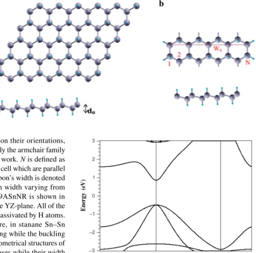
of NRs are distinguished depending on their orientations, namely, armchair and zigzag NRs. Only the armchair family of nanoribbons is investigated in this work. N is defined as the number of Sn–Sn dimer in the unit cell which are parallel to the axis of the nanoribbons, the ribbon’s width is denoted by Wa . We consider the ASNRs with width varying from
N = 7 to N = 17 . The super cell of 9ASnNR is shown in
Fig. 1. ASnHNRs are considered in the YZ-plane. All of the dangling bonds on the edge sites are passivated by H atoms.
Compared to the stanene structure, in stanane Sn–Sn bond and lattice constant are increasing while the buckling decreases [24]. Investigation of the geometrical structures of ASnHNRs shows the buckling decreases while their width increases.
4 Electronic properties of stanane
and ASnHNRs
Figure 2 presents the computed electronic band structure of stanane along K − Γ − M − K direction. The band gap of stanene is 0.04 eV, however, adsorption of hydrogen on stanene has significant effect on its electronic properties. Here, our calculations for electronic band structure of stan-ane show that it is a semiconductor with a direct band gap of 1.22 eV at Γ point, Fermi level is shifted to zero. This moderate value of band gap makes stanane a good candidate for various applications. There is a twofold degeneracy at Γ point of valance band.
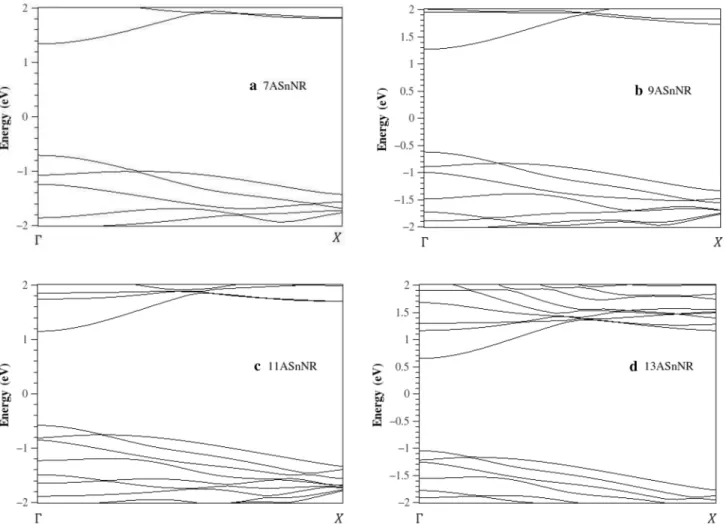
The band structure of some ASnHNRs in the absence of spin–orbit interaction (SOI) are shown in Fig. 3. In all band structure diagrams, the Fermi level is shifted to zero. The value of the ASnHNRs band gap differs from that of parent 2D structure due to the combined effect of quantum confine-ment. These structures were observed to be semiconductors with a direct band gap at Γ point.
The number of bands near Fermi level increases with increasing the ribbon’s width. It is also observed that
valence maximum band (VBM) and conduction band minimum (CBM) are inhomogeneous related to Fermi level. Band gap reduces with increases in the ribbon’s width. For accurate investigation, we plotted the varia-tion in band gap as a funcvaria-tion of ribbon’s width for 7–17 ASnHNRs which is presented in Fig. 4.
By comparing the variation of band gap in ASnHNRs with armchair stanene nanoribbons, which we investi-gated in our previous work [33], it is observed that here the quantum confinement effect is not as emphasized as that found in stanene nanoribbons. We also calculated the density of states (DOS) of ASnHNRs. As shown in Fig. 5, the DOS spectra for different ASnHNRs are similar except for small differences in their shapes and amplitudes. As the ribbon’s width increases, the energy of states near Fermi level is shifted upward. This shift leads to a decrease in the size of band gap [18].
Fig. 1 (Color online) Top and side view of a 2D stanane SnH layer, buckled height of stanane is denoted by d0 , b super cell of
9ASnHNR, Wa is the ribbon’s width and N shows the number of dimer lines along the ribbon direction. The gray and the blue balls represent tin and hydrogen atoms, respectively
Fig. 2 Band structure of stanane SnH in the absence of spin–orbit interaction SOI, Fermi level is shifted to zero
Fig. 3 The band structure of a 7ASnHNR, b 9ASnHNR, c 11ASnHNR and d 13ASnHNR in the absence of spin–orbit interaction
Fig. 4 variation of band gap as the ribbon’s width. As the ribbon’s width increases, the size of band gap decreases
Fig. 5 (Color online) Density of state DOS of 7-, 11-, 15 ASnHNRs. By increasing the ribbon’s width, energy of states near Fermi level is shifted upward
5 Optical properties of stanane
and ASnHNRs
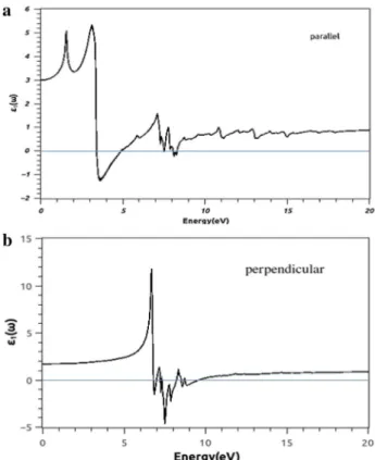
Stanane is a promising candidate for optoelectronics because of its moderate direct band gap, [10]. Therefore, we calculated the imaginary and real part of dielectric function for both stanane and ASnHNRs. Our calculations were done for two directions of incident light polariza-tions, parallel and perpendicular to structures. For the parallel polarization, as shown in Fig. 6a, the calculated
𝜀2(𝜔) of stanane in the band gap area is zero, but in all
other energies, there are peaks indicating the absorption of light. The major peak shows that stanane has a pro-nounced visible light and UV light adsorption. Therefore, it posses great potential in photo-related applications. In stanene, the main peaks are located at 5eV and continue up to 10 eV with very low intensity [24]. Then, for this direc-tion of polarizadirec-tion, adding hydrogen to stanene causes an increase in the imaginary part of the dielectric field. This enhancement will definitely affect on absorption. When polarization is perpendicular, as shown in Fig. 6b,
𝜀2(𝜔) is zero in visible light region and here are two main
peaks between 6.5 and 7.5 eV. As it is observed, stanane exhibits remarkable decrease in light adsorption for the perpendicular polarization compared to parallel. Actually, adsorption of hydrogen on stanene has significant effect on its electronic properties since it helps the saturation of
bonds, hence, stanane is a semiconductor with direct band gap at gamma point. So, the effect of this modified band structure is evident on the optical properties. On the other hand, the difference in light absorption for the perpendicu-lar poperpendicu-larization compared to parallel one is a consequence of the buckling and two-dimensional nature of the stanane. The effect of anisotropy of the structure is very apparent from this absorption spectra. Clearly, the transitions from occupied valance states to unoccupied conduction states, the optical matrix elements, are forbidden or very weak apart from 5 to 10 eV range for perpendicular polarization. Generally, in fully hydrogenated stanene optical spectrum comparison with stanene, peaks have higher intensity, but they are limited to the smaller. It means that, by adding hydrogen to stanene, we can make a good transparent material.
The real part of dielectric function of stanane was also investigated for two directions of light polarization.
As shown in Fig. 7, there are dips in the amplitude of
𝜀1(𝜔) , and some of them attain a small negative value. When 𝜀(𝜔) is real and negative no radiation can propagate [31].
The negative values indicate the plasmonic excitation. There is only a small negative value in 𝜀1(𝜔) for the polarization parallel to the stanane rages of 3.5–5.0 eV. The negative values for the perpendicular polarization are greater com-pared to the parallel polarization’s values, and they are seen
Fig. 6 The imaginary component of the dielectric function of stanane
par-in the range of 6.7–10 eV. Thus, par-in this range, no radiation can propagate. It is also observed that the static dielectric constant (value of 𝜀1(𝜔) at zero energy) equals to 1.8 for perpendicular, and it equals 3 for parallel polarization. The differences between the perpendicular and the parallel real parts of dielectric function confirm the anisotropic behavior of optical properties. After dielectric function, we presented the absorption spectra of stanane in Fig. 8. The presence of cutoff energy here confirms the presence of band gap in the band structure.
For parallel polarized light, there are several peaks at high intensity in all ranges of incident light energy. In com-parison with the stanene, hydrogenated stanene is more absorptive, especially for higher energies. For perpendic-ular polarization, our results from Fig. 8 indicate strong light transmission in 0–5 eV and absorption in the range of 6–10 eV. Absorption peaks originate of two main transi-tions between electronic states. Actually, the broad of these peaks corresponds to the transitions from ∏ to ∏∗ for the first peak and 𝜎 to 𝜎∗ for the second one. The results of our calculations for the optical properties of stanane show that they strongly depend on the direction of light’s polarization.
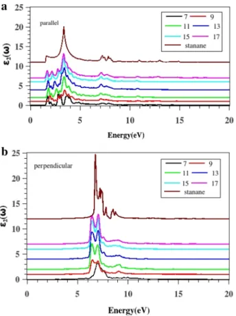
This anisotropic manner in stanane is more pronounced than stanene [24]. In the following, we investigate the optical properties of ASnHNRs. Figure 9 shows the imaginary part of dielectric function for the ASnHNRs. In the band gap area, 𝜀2(𝜔) spectrum is zero. In the case of parallel polariza-tion, transitions are happen for the energies more than band gap energies immediately. This means that for the paral-lel polarization ASnHNRs can absorb the electromagnetic waves if their energy is more than 1.5 eV. Several oscil-lations are seen in the range of 1.5–5 eV. There are two peaks in 6.5–8.5 eV which also have low amplitude. With increasing the nanoribbons’ width, the number of peaks in this region decreases and a main peak grows between 3 and 4 eV. In stanane, these small peaks vanish completely and they change to a broader peak. The amplitude (intensity) of all peaks increase with the increasing of the nanoribbons’ width, and all peaks also shift to the lower energies. For the perpendicular polarized, light peaks are in the range of 5–11 eV. However, up to 5 eV and also above 11eV 𝜀2(𝜔) goes to zero. When the ribbons’ width is increased, the peaks are centralize. This means that there is no absorp-tion at either low or high frequency. Then, for this direcabsorp-tion of polarization, ASnHNRs have a different manner. They
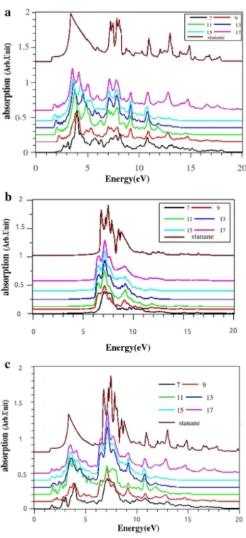
Fig. 8 Absorption spectra of stanane for a parallel b perpendicular-polarized light
Fig. 9 (Color online)The imaginary portion of the dielectric func-tion of ASnHNRS for a parallel b perpendicular polarizafunc-tion. Labels show the number of dimer lines along the ribbon direction
are transparent for a wide range of energy, and they can be used as a transparent conducting film (TCF). Additionally, they can act as important elements in a number of electronic devices including liquid-crystal displays, OLEDs, touch-screens, and photovoltaics. As we expected, 𝜀2(𝜔) and 𝛼(𝜔) are very similar. This matter can be confirmed by comparing the imaginary part of the complex dielectric function shown in Fig. 9 and the optical absorption coefficient displayed in
Fig. 10. First of all, it is evident that the optical properties of ASnHNRs are anisotropic with respect to the type of light polarization from the comparison of Fig. 10a and Fig. 10b. The differences between two polarizations are a consequence of the selection rules raised from the electronic dipole transi-tion matrix elements. In Fig. 10c, we show the absorption for unpolarized light. Different peaks with various heights are seen in a wide range. The highest peaks are located between 6-9 eV. For unpolarized light, both stanane and ASnHNRs are good absorptive.
6 Conclusions
In conclusion, we have studied the structural, electronic, and optical properties of fully hydrogenated stanene, stanane, and armchair stanane nanoribbons (ASnHNRs) by DFT-based calculations. Our investigations show that stanane is a semiconductor with the direct band gap of 1.2 eV. This moderate value of the band gap makes stanane a good candi-date for various applications. ASnHNRs are semiconductors with a wide direct band gap, and their band gap decreases with the increasing nanoribbons’ width due to the quantum confinement effect. An investigation of optical properties proves that the dielectric function strongly depends on the polarization’s direction of incident light. Both stanane and ASnHNRs have a completely different manner in absorption for two directions of polarization. They are good absorptive matter for parallel direction and transparent for the perpen-dicular polarized light.
Acknowledgements We acknowledge support by the Scientific and Technological Research Council of Turkey (TÜBİTAK), Grant No. (117F097) and by the EU-COST Action (CA16221).
References
1. Y. Zhang, Y.-W. Tan, H.L. Stormer, P. Kim, Experimental obser-vation of the quantum Hall effect and Berry’s phase in graphene. Nature 438(7065), 201–204 (2005). https ://doi.org/10.1038/natur e0423 5
2. C. Lee, X. Wei, J.W. Kysar, J. Hone, Measurement of the elas-tic properties and intrinsic strength of monolayer graphene. Sci-ence 321(5887), 385–388 (2008). https ://doi.org/10.1126/scien ce.11579 96
3. Y.S. Dedkov, M. Fonin, Electronic and magnetic properties of the graphene-ferromagnet interface. New J. Phys. 12(12), 125004 (2010). https ://doi.org/10.1088/1367-2630/12/12/12500 4 4. L. Jiao, L. Zhang, X. Wang, G. Diankov, H. Dai, Narrow graphene
nanoribbons from carbon nanotubes. Nature 458(7240), 877–880 (2009). https ://doi.org/10.1038/natur e0791 9
5. M.Y. Han, B. Özyilmaz, Y. Zhang, P. Kim, Energy. Phys. Rev. Lett. 98(20), 206805 (2007). https ://doi.org/10.1103/PhysR evLet t.98.20680 5
Fig. 10 (Color online)Absorption spectra of ASnHNRs for polariza-tion of light a along ASnHNRs, b perpendicular to the ribbons plane, c unpolarized
6. Z. Chen, Y.-M. Lin, M.J. Rooks, P. Avouris, Graphene nano-rib-bon electronics. Phys. E Low-dimension. Syst. Nanostruct. 40(2), 228–232 (2007). https ://doi.org/10.1016/j.physe .2007.06.020 7. V. Barone, O. Hod, G.E. Scuseria, Electronic. Nano Lett. 6, 2748–
2754 (2006). https ://doi.org/10.1021/nl061 7033
8. C. Ataca, S. Ciraci, Perpendicular growth of carbon chains on gra-phene from first-principles. Phys. Rev. B 83(23), 235417 (2011). https ://doi.org/10.1103/PhysR evB.83.23541 7
9. A.M. Suarez, Theory and simulation of atomic hydrogen, fluo-rine, and oxygen on graphene. https ://etda.libra ries.psu.edu/catal og/15218
10. Z. Wang, J. Xiao, M. Li, Adsorption of transition metal atom on zigzag graphene nanoribbon. Appl. Phys. A 110(1), 235–239 (2013). https ://doi.org/10.1007/s0033 9-012-7119-8
11. Y.H. Lu, W. Chen, Y.P. Feng, P.M. He, T. Tuning, J. Phys. Chem. B 113(1), 2–5 (2009). https ://doi.org/10.1021/jp806 905e 12. V. Barone, O. Hod, G.E. Scuseria, Electronic. Nano Lett. 6(12),
2748–2754 (2006). https ://doi.org/10.1021/nl061 7033
13. A. Martín, P. Batalla, J. Hernández-Ferrer, M.T. Martínez, A. Escarpa, Graphene oxide nanoribbon-based sensors for the simul-taneous bio-electrochemical enantiomeric resolution and analy-sis of amino acid biomarkers. Biosens. Bioelectron. 68, 163–167 (2015)
14. F. Schedin, A.K. Geim, S.V. Morozov, E.W. Hill, P. Blake, M.I. Katsnelson, K.S. Novoselov, Detection of individual gas mol-ecules adsorbed on graphene. Nat. Mater. 6(9), 652–655 (2007). https ://doi.org/10.1038/nmat1 967
15. S. Guo, Graphene-Based Material Systems for Nanoelectronics and Energy Storage Devices, Ph.D. thesis, UC Riverside (2012). https ://escho larsh ip.org/uc/item/0qk8m 6q5
16. A. Candini, S. Klyatskaya, M. Ruben, W. Wernsdorfer, M. Affronte, Graphene spintronic devices with molecular nanomag-nets. Nano Lett. 11(7), 2634–2639 (2011). https ://doi.org/10.1021/ nl200 6142
17. Y.-E. Yang, Y.-R. Yang, X.-H. Yan, Universal optical properties of graphane nanoribbons: a first-principles study. Phys. E Low-dimension. Syst. Nanostruct. 44, 1406–1409 (2012). https ://doi. org/10.1016/j.physe .2012.03.002
18. Y. Li, Z. Zhou, P. Shen, Z. Chen, Structural and electronic proper-ties of graphane nanoribbons. J. Phys. Chem. C 113(33), 15043– 15045 (2009). https ://doi.org/10.1021/jp905 3499
19. H. Okamoto, Y. Sugiyama, H. Nakano, Synthesis and modification of silicon nanosheets and other silicon nanomaterials. Chem. Eur. J. 17(36), 9864–9887 (2011). https ://doi.org/10.1002/chem.20110 0641
20. F.-F. Zhu, W.-J. Chen, Y. Xu, C.-L. Gao, D.-D. Guan, C.-H. Liu, D. Qian, S.-C. Zhang, J.-F. Jia, Epitaxial growth of two-dimen-sional stanene. Nat. Mater. 14(10), 1020–1025 (2015). https ://doi. org/10.1038/nmat4 384
21. S. Saxena, R.P. Chaudhary, S. Shukla, Stanene: atomically thick free-standing layer of 2d hexagonal tin. Sci. Rep. 6, 31073 (2016). https ://doi.org/10.1038/srep3 1073
22. M. Modarresi, A. Kakoee, Y. Mogulkoc, M.R. Roknabadi, Effect of external strain on electronic structure of stanene. Comput. Mater. Sci. 101, 164–167 (2015). https ://doi.org/10.1016/j.comma tsci.2015.01.039
23. N.J. Roome, J.D. Carey, Beyond graphene: stable elemental mon-olayers of silicene and germanene. ACS Appl. Mater. Interfaces 6, 7743–7750 (2014). https ://doi.org/10.1021/am501 022x 24. M. Fadaie, N. Shahtahmassebi, M.R. Roknabad, Effect of external
electric field on the electronic structure and optical properties of stanene. Opt. Quant. Electron. 48(9), 440 (2016). https ://doi. org/10.1007/s1108 2-016-0709-5
25. W. Wei, Y. Dai, B. Huang, T. Jacob, Many-body effects in silicene, silicane, germanene and germanane. Phys. Chem. Chem. Phys. 15(22), 8789–8794 (2013). https ://doi.org/10.1039/C3CP5 1078F 26. K.L. Low, W. Huang, Y. Yeo, G. Liang, Ballistic transport per-formance of silicane and germanane transistors. IEEE Trans. Electron. Dev. 61(5), 1590–1598 (2014). https ://doi.org/10.1109/ TED.2014.23130 65
27. H.L. Zhuang, A.K. Singh, R.G. Hennig, Computational discovery of single-layer III–V materials. Phys. Rev. B 87, 165145 (2013) 28. B. Peng, D. Zhang, H. Zhang, H. Shao, G. Ni, Y. Zhu, H. Zhu,
The conflicting role of buckled structure in phonon transport of 2d group-IV and group-V materials. Nanoscale 9(22), 7397–7407 (2017)
29. B. Peng, H. Zhang, H. Shao, Y. Xu, X. Zhang, H. Zhu, Low lattice thermal conductivity of stanene. Sci. Rep. 6, 20225 (2016) 30. P.B. Johnson, R.W. Christy, Optical. Phys. Rev. B 6(12), 4370–
4379 (1972). https ://doi.org/10.1103/PhysR evB.6.4370 31. P. Ravindran, A. Delin, B. Johansson, O. Eriksson, J. Wills,
Elec-tronic structure, chemical bonding, and optical properties of fer-roelectric and antiferfer-roelectric nano 2. Phys. Rev. B 59(3), 1776 (1999)
32. S.-S. Li, C.-W. Zhang, Tunable electronic structures and magnetic properties in two-dimensional stanene with hydrogenation. Mater. Chem. Phys. 173, 246–254 (2016). https ://doi.org/10.1016/j.match emphy s.2016.02.010
33. M. Fadaie, N. Shahtahmassebi, M.R. Roknabad, O. Gulseren, First-principles investigation of armchair stanene nanoribbons. Phys. Lett. A 382(4), 180–185 (2018). https ://doi.org/10.1016/j. physl eta.2017.11.018
Publisher’s Note Springer Nature remains neutral with regard to jurisdictional claims in published maps and institutional affiliations.