Copyright © 2008 American Scientific Publishers All rights reserved
Printed in the United States of America
Journal of Nanoscience and Nanotechno/agy Vol. 8, 510—517, 2008
A Figure of Merit for Optimization of
Nanocrystal Flash Memory Design
Aykutlu Dana‘, Imran Akcal, Atilla Aydinlil’t‘, Rasit Turanz, and Terje G. Finstad3
1Department of Physics, Bi/kent University, 06800 Ankara, Turkey2Department of Physics, Middle East Technical University, 06800 Ankara, Turkey 3Department of Physics, University of Oslo, RBOX 1048 — Blindern, 0316 Oslo, Norway
Nanocrystals can be used as storage media for carriers in flash memories. The performance of a nanocrystai flash memory depends critically on the choice of nanocrystai size and density as well as on the choice of tunnel dielectric properties. The performance of a nanocrystai memory device can be expressed in terms of write/erase speed, carrier retention time and cycling durability. We present a model that describes the charge/discharge dynamics of nanocrystai flash memories and calculate the effect of nanocrystai, gate, tunnel dielectric and substrate properties on device performance. The model assumes charge storage in quantized energy levels of nanocrystals. Effect of temperature is included implicitly in the model through perturbation of the substrate minority carrier concentration and Fermi level. Because a large number of variables affect these performance measures, in order to compare various designs, a figure of merit that measures the device performance in terms of design parameters is defined as a function of write/erase/discharge times which are calculated using the theoretical model. The effects of nanocrystai size and density, gate work function, substrate doping, control and tunnel dielectric properties and device geometry on the device performance are evaluated through the figure of merit. Experimental data showing agreement of the theoretical model with the measurement results are presented for devices that has PECVD grown germanium nanocrystals as the storage media.
Keywords: Nanocrystals, Germanium, PECVD, Germanosilicate, Capacitance Spectroscopy, Memory, Retention.
1. INTRODUCTION
Nanocrystals (NCS) formed by annealing silicon diox-ide films having excess Si or Ge has attracted much attention due to optical and electronic properties of such nanostructures.“3 In particular, NCs embedded in silicon oxide films have been subject of study for their potential applications in memory devices.4 Among various methods of synthesis of the NCs are, ion implantation into oxide, co-sputtering of oxide and germanium (Ge), low pressure chemical vapor deposition (LPCVD) and plasma enhanced chemical vapor deposition (PECVD) followed by appro-priate annealing of the grownfilms.5‘6 Since many param-eters of NCs such as density, size, and composition can be adjusted by proper choice of deposition parameters, NCs offer flexibility in design offlash memory cells. However, understanding of charge storage mechanisms is important in optimization of device performance.
*Author to whom correspondence should be addressed.
In this paper, we analyze nanocrystal memory charg-ing and retention dynamics by assumcharg-ing carrier storage in NC energy levels instead of deep traps. Based on this assumption, we present a theoretical model that includes the effect of NC dimensions and density to calculate the charging and discharging dynamics. Gate work function, substrate doping and tunnel dielectric properties are inher-ently included. This study is restricted to electron storage in Ge NCs for the sake of simplicity. The analysis can be extended to Si NCs by adjustment of material parameters, and can further be extended for hole storage in Si and Ge NCs with proper adjustment of the band-bending model.
2. THEORETICAL MODELLING
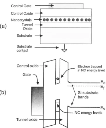
A typical nanocrystal metal—oxide-semiconductor (NC-MOS) memory element consists of a standard MOS capac— itor with a layer of NCs embedded in the oxide between the gate and the substrate as shown in Figure 1.
Based on the assumption that only NCs are responsible for charge storage and that a single electron per NC is
Drina er a]. A Figure of Merit for Optimization of Nanocrystal Flash Memory Design Control Gate —l—>——l Control Oxide “—F’ Nanocrystals —l* O. C O O I Q C O O .9 Tunnel —> (a) Oxide Substrate —> Substrate —, é contact Control oxide —— Gate 1 Electron trapped in NC energy level Si substrate bands Ev NC energy levels Tunnel oxide —
Fig. 1. Typical nanocrystal MOS capacitor memory test element with an n-type substrate. (a) Cross-section and (b) band diagram of charged element under 0 V bias.
stored for a total of nNC NCs, the flat-band voltage shift AVFB is approximately given by7
n E t
AVFB:%<tcox+ 0X DC) (1)
ox 2 Ege
where q is the electronic charge, rm is the control oxide thickness, rm is the average diameter of the NCs, E’s are the dielectric constants of respective materials.
In order to evaluate dynamical properties of such mem-ory elements, charging and discharging currents must be calculated taking into account tunnelling through the bar-rier for a given electric field within the tunnelling region. The currents also depend on availability of source and tar-get states. Since therc are many device parameters that c01— lectively determine the charge-discharge currents, a simple closed form formula can not be obtained that covers all cases. Therefore, in the following subsections, charge and discharge currents are studied separately, and intuitive for-mulas are given whenever possible.
2.1. Charging of the NC-MOS Element
It is best to capture the essential features of charging dynamics with a minimally complex model. During the write cycle, the device is in accumulation and initially there is no stored charge in the device. In this case, the oxide field m will be determined by the gate voltage during writing, Vwmc, approximately as E())( 2 write/10x,
J. Nanosci. Nanotechnol. 8, 510—517, 2008
where t0X is the total effective oxide thickness. The tun-nelling current through a trapezoidal barrier can be cal-culated in two different limits, the direct tunnelling and Fowler-Nordheim limits. It should be noted that, it is desir-able to have low fields in flash memory devices in order to increase device reliability. In the case of direct tunnelling, charging current density can be calculated using a trans— mission coefficient which can be calculated by the WKB approach for direct tunneling. The charging current density
then becomes8
AF2
F t
3/2 13s
Jc : tox X exp __ 1 _ (1 _ tox 10x) > B (2)
VB VB Flex
where A : qzmsi/l6772moxh, B : 2,/8moxq/3h, E0x is the
tunnel oxidefield during charging, mox is the tunnel effec-tive mass and VB is the barrier height between the oxide and the substrate. At high fields (Fmttox > VB) the tun-nelling is through a triangular barrier (FN regime) and the tunnel transparency term in Eq. (2) must be rewritten, resulting in a charging current density given by9
n/z
F l
[0X 2’4o
[
JC = — x exp — VB(3)
The actual charge deposited will depend on the availabil-ity of final states. This can be accounted for by including a capture cross section per nanocrystal. The differential charge deposited per unit area do in a time interval d7 can be calculated through
d0=PcD JAE )d7
trap 0x(4)
where pc is the average capture cross section, and Dtrap is the available density of target states. The capture probabil-ity may depend on NC shape and Dtrap % NNC is the NC area] density.
2.2. Discharging of the NC-MOS Element
During retention, the device is in depletion and ne : 0. If NC bound states are responsible for storage of carri-ers, discharge occurs by tunnelling from the NC ground state to the substrate, either by direct or trap assisted tunnelling. For the case of direct tunnelling, the current density describing the discharge of the NCs is different than Eq. (2) mainly because available source states are not a bulk continuum but are the NC states. Assuming a delta-function distribution for the NC states DNC(E) : NNC6 (E — ENC) located at the quantization energy ENC and a single stored carrier for every NC, the discharge current density can be given as
Jd = qNNCTi(ENC)UNC (5)
where UNC z i‘nr/Zritgcd2 is the semi-classical escape attempt rate for NCs of diameter (1.10
A Figure of Merit for Optimization of Nanocrystal Flash Memory Design Drina e! a].
The transmission probability TI(E,FW) for a single electron at energy E can be calculated through the WKB approximation as
,V ottox 3/2 BVB(E)3/2
‘<E)~4e*pl‘(l*(l"v;m> )‘F—l ‘6)
[OKThe tunnel oxide field is determined by the amount of stored carriers as well as by the band-bending. For a given stored charge, the oxide field therefore depends on the tun-nel oxide thickness, total oxide thickness, substrate dop— ing, gate work-function and dielectric constants. In order to obtain an intuitive result, we consider the case where stored charge is small and tunnel oxide field is proportional to the stored charge (or flat—band shift), Fl0x Q: AVFB/2t0x.
For the calculation of the discharge current through Eqs. (5) and (6), the barrier height must also be calcu-lated. The barrier height is a function of the NC ground state energy given by VB(E) = VBO— NC, where VBO is the bulk barrier height. The energy levels of uncapped ger-manium NCs have recently been measured directly as a
function of size, using scanning tunnelling spectroscopy.ll
An empirical formula for the conduction band minimum of Ge NCs as a function of size is given by
11.86 d2+1.51d+3.3936 where the energies are in eV, d is the nanocrystal diameter in rim. Equation (7) can be used to estimate ENC, which can be used in the estimation of the tunnelling barrier observed by the NCs during discharge.
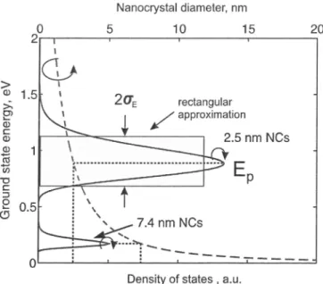
The size distribution of NCs leads to a distribution of energies. Considering a Gaussian size distribution, a den-sity of states (DOS) can be calculated (Fig. 2). The DOS can also be approximated by a Gaussian. In this case, the stored charge is distributed to the available NC states according to Fermi-Dirac distribution with a local quasi-Fermi level. For a Gaussian density of states with peak energy Ep and half width of (TE, the quasi-Fermi level of the nanocrystal ensemble is given in the zero temperature limit by
ECBM (d) 2 ECBM (00) ‘l‘ (7)
2
EF 2 EP +
fiaE x Erf“ (Nnc — 1)
(8)
NC
where E rf ‘1 denotes the inverse of the error—function, nC is the total number of stored carriers and NNC is the total number of nanocrystals. The quasi—Fermi depends strongly on the ratio of total stored charge to number of NCs.
Escape of carriers near or above the quasi-Fermi level dominates the discharge current. Therefore, discharge cur-rent depends on the number of stored carriers which is proportional to the flat—band voltage shift through Eq. (1). This feature of the escape current is the reason of super-exponential charge decay in NC memory elements. A more intuitive, closed-form formula for the discharge current is
Nanocrystal diameter, nm 0 5 10 15 20 rectangular / approximation 2.5 nm NCs Ground state energy, eV
Density of states , a.u.
Fig. 2. Schematic description of density of states (solid curves) for the ground states of nanocrystals with two representative average diameters of 2.5 and 7.4 nm. Minimum of energy corresponds to the conduction band edge of bulk germanium. Dotted curve shows electron ground state of NCs as a function of size as described by Eq. (7). Areas under the curves are equal to the NC area] density.
desirable to compare the effect of design parameters on charge retention. However, a simple closed-form expres-sion can not be obtained without further simplifying assumptions. A closed-form formula can be obtained by assuming a rectangular shaped density of states, neglect-ing band bendneglect-ing effects, assumneglect-ing a gate work-function that is aligned with the substrate Fermi level and calcu-lating in the zero temperature limit. Then Eq. (8) can be approximated by
2 .
EF=EP+«/2(IE(NH‘ —1)
(9)
NC
Under these assumptions, Eqs. (5), (6), and (9) can be used to calculate a closed form for the discharge current at zero gate bias. The discharge current is then given as a function of the flat-band voltage shift AVFB due to stored carriers as J N 4qNNC7Th\/Vpexp[—%Btmx\/Vp] d _ 3mgedzBrmaE 331mmE AVFB ———-_—-—— —l 10
X(exp( 2m AV...“
( )
where Vp : VB —Ep / q is the barrier height observed by the average size NC, 0'E is the width of the rectangular energy distribution, rm is the tunnel oxide thickness, mg‘.' is the electron mass in the nanocrystal, AVmaX 2 qNNCrox/ 60X is the maximumfiat-band voltage shift when all nanocrystals carry an electron, and B = 4\/2moxq/3h, mOX being the electron tunnelling mass. Note that V1: and (TE are normal— ized by q, to have units of Volts.
Dana 61 al. A Figure of Merit for Optimization of Nanocrystal Flash Memory Design
The approximate discharge current density given by Eq. (10) includes the effects of NC density, size distribu-tion, flat—band voltage shift as well as tunnel oxide thick-ness and tunnel barrier height.
2.3. Temporal Decay of Stored Charge
The time decay of the NC charge can be calculated through
integration of Eq. (10) which is of the form Jd(AVFB) :
Jd0(exp(/3AVFB) — l). The retention time Tm is found as a function of initial and final flat-band voltage shifts as
ox <65“ _ 1 Vi ~ Vf
TI'CI : — In 7— * 0X
JdOB efih — 1 Jdt)
where Vi is the initial fiat—band shift before decay, Vf
is the final flat-band shift at time Tm, B = 3BtmaE/
2/WAVWX is as given in Eq. (10). The factor Jdo can be referred from Eq. (10) and COx is the device capacitance per unit area.
(11)
2.4. Figure of Merit for a Nanocrystal Memory Cell
The figure of merit (FOM) definition chosen in this
article is
Tret JC
FOMziog10
:loglo —
(12)
Tcharge Jd
where "rm and Tcmge are the retention and charging times for a given set of device parameters. The FOM depends on many design parameters such as the write voltage Vwme, desired retention time Tm, desiredflat—band voltage shift at the end of retention time Vf, tunnel barrier properties such as width, dielectric constant and barrier height, control dielectric properties such as width and dielectric constant, substrate doping, gate work-function, nanocrystal size dis— tribution and material composition. The effects of some of the parameters are interrelated through non-linear equa-tions and only a numerical result for the FOM can be obtained without simplifying assumptions. Using numer— ical calculation, the FOM can be calculated for a given device geometry (control and tunnel barrier thicknesses) and nanocrystal size distribution. A greater FOM will mean a faster device writing time, Tcharge. A FOM of about 18 is desirable which means a nanosecond write time for 10 year data storage.
3. EXPERIMENTAL DETAILS 3.1. Sample Preparation
The oxide-germanosilicate—oxide trilayerfilms were grown in a PECVD reactor (model PlasmaLab 8510C) on Si sub-strates using 180 seem SiH4 (2% in N2), 225 sccm NO2
and varying flow rates of GeH4 (2% in He) as
precur-sor gases, at a sample temperature of 350 °C, a process J. Nanosci. Nanotechnol. 8, 510—517, 2008 a" E)
a
b
c
, :15” ,. ‘X‘ W3 mxwgkv‘w ; .1 .;~Fig. 3. Formation of Ge NCs as a function of anneal temperature and GcH4 flow rate as observed by TEM. Multi-laycr structures of ger— manosilicate with flow rates of 120. 110, 100, and 90 seem are seen away from the substrate (bottom to top) after annealing at (a) 650 “C, (b) 770 °C, and (c) 850 °C for 5 minutes.
pressure of 1000 mTorr under and an applied RF power of 10 W. The samples were then annealed in N2 atmo-sphere in an alumina oven at temperatures ranging from 650 °C to 950 °C for 5 minutes. The samples were loaded and unloaded with ramp times of 1 minute.
Transmission electron microscopy (TEM) images of a multilayered test sample show the formation of NCs as a function of annealing temperature as seen in Figure 3. The layers contain increasing amounts of Ge in layers away from the silicon substrate. High density NC formation is observed only in the bottom-most layer which has a com-position of SiObGeMO2 as determined by XPS analysis. The NC diameter increases nonlinearly from 2.5 nm to 7.4 nm as the annealing temperature is increased from 650 °C to 850 °C as tabulated in Table I. For fabrication of the devices, first a thermal tunnel oxide of thickness 4 nm was grown using dry oxidation, followed by PECVD growth of germanosilicate layer of 10 nm thickness and composition of SiofiGeMO2 were grown on n-type silicon substrates with resistivity of 1—10 0 cm. This germanium rich layer is where NCs form upon annealing. On top, a Icon = 17 nm control oxide was deposited. Backside ohmic metallization was done by Aq evaporation for the n—type substrates followed by rapid thermal annealing in forming gas. Gate metallization was done by shadow evaporation of aluminium.
3.2. Flat-Band Voltage Measurement
Capacitance measurements were performed using a capac-itance meter (HP 4278A) using 1 MHZ AC excitation with 25 mV amplitude. The flat-band voltage shift can be tracked quasi-real-time for small changes in the flat—band shift by using a digital feedback loop that we developed. The feedback loop operates by measuring the capacitance and using successive approximation tofind the value of the 513
A Figure of Merit for Optimization of Nanocrystal Flash Memory Design aa e! a].
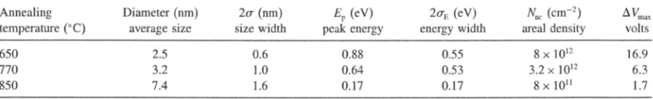
Table I. Average nanocrystal size and width of size distribution for different annealing temperatures as observed by TEM. Equation ('7) is used to estimate peak ground state energy and width of density of states distribution for the nanocrystal ensemble.
Annealing Diameter (nm) 20' (nm) EP (eV) 20,-: (eV) Nm. (cm'z) AV”x
temperature (°C) average size size width peak energy energy width areal density volts
650 2.5 0.6 0.88 0.55 8 x 10¹² 16.9
770 3.2 1.0 0.64 0.53 3.2 X 10¹² 6.3
850 7.4 1.6 0.17 0.17 8x10ll 1.7
gate bias required to observe a given set—point capacitance value and eliminates the need of tracing the whole CV curve and post-processing of the data to access the value of the flat—band voltage shift. During write/erase pulses, the loop can be momentarily turned off, and after the pulse it can be restarted at the same bias voltage. This method allows rapid monitoring of the changes in the flat—band voltage shift (within few tens of msec) after a write or erase pulse. The flat—band voltage difference can be mea— sured rapidly and can be used to extract the discharge or charge currents.
3.3. Charging of Nanocrystals
Dynamic CV measurements have been performed on NC-MOS capacitors, by measuring the CV as a func— tion of time near the fiat-band voltage between applied pulses of varying pulse voltage and afixed pulse duration 50 msec.
As can be seen in Figure 4, the total accumulated charge measured through flat-band voltage shift follows the nano— crystal density, which is proportional to l/dgc.
The charging currents are extracted from flat—band volt— age shift measurements, by applying a 12 V write pulse to previously uncharged three devices with properties shown in Table I. The experimental values of JC are 8.68 nA, 4.76 nA, and 0.73 nA per cm2 for devices with NC densities of 8 x 10¹², 3.2 X 10¹², and 8 x 1011 cm—2 ‘1
10
% 10°— ‘fi... A
—
>
>
"a;
<1 10‘1-
—
—21o
-
'
.
2 4 6 8 10 average diameter, nmFig. 4. Flat-band voltage shift as a function of nanocrystal diameter (filled triangles) and for the as deposited sample (horizontal dotted line) after a 7 V write pulse of duration 500 msec. The dotted curve is drawn to aid the eye.
respectively. The current density calculated using Eq. (2) is
21 nA cm‘2 using oxide properties found in literature.912
Remarkable proportionality of charge current density to NC density shows that capture cross section pC is rather independent of NC size for our NCs and has a value of
about 5 x 10’14 cm2. Discharge current Jd, Acm'z 10 -10-18 l 1 l l l o 0.5 1 1 5 2 2.5 3 10’6 , . . . . (b) 10'9- _ Discharge Current density, Jd Acm—2
Fig.5. (a) Discharge currents as a function of fiat-band voltage shift calculated for NC—MOS devices under zero gate bias. A tunnel oxide thickness of 4 nm and total oxide thickness of 31 nm is assumed. Bulk barrier height of oxide-silicon inteli‘ace is taken as 3.3 eV. Nanocrystal parameters are based on experimental values given in Table 1. Solid curves are the currents for the rectangular DOS approximation given in Eq. (10) and dashed curves are numerical results assuming Gaussian DOS. (b) Experimental discharge current densities at zero gate bias plot-ted as a function of flat—band voltage shift for 2.5, 3.2, and 7.4 nm nanocrystals. Dashed lines are linear interpolations drawn to aid the eye.
aa er al. A Figure of Merit for Optimization of Nanoerystal Flash Memory Design
3.4. Discharging of Nanocrystals
The discharge currents have been measured through decay of stored Charge for the three devices as shown in Figure 5(b).
The discharge current densities are plotted in Fig— ure 5(a). It is seen that Eq. (10) agrees reasonably well with a more accurate numerical calculation for small ratios of AVFB/AVmax < 0.2. If charging ratio is large, i.e., when AVFB/AVmax —> 1, the rectangular DOS approxima-tion breaks down. Still, Eq. (10) can be used to estimate effect of design parameters on the retention performance by careful consideration of the value of AVFB/AVmaX for the desired memory window. For example, noting the dependence of Ep given in Eq. (7), it can be seen from Eq. (10) that an increasing NC diameter increases the aver-age barrier height and reduces the discharge current. It can also be seen that, increasing NC density but keep-ing other parameters constant increases AVnm, which in turn gives a lower quasi-fermi level for carriers in NCs for the same memory window, and reduces the escape current.
The smaller NCs can hold more charge due to increased NC density but they also decay faster. Comparison of Figures 5(a, b) shows that the numerical solution pre-dicts the discharge currents rather accurately. For exam— ple, it is seen that, as the flat-band voltage nears 1.7 volts (AVmax for the 7.4 nm device), there is a sharp increase in the experimental discharge current. This is in accor— dance with the numerical solution. Also, size dependence of the discharge currents are similar for theory and experi-ment. Therefore, we conclude that the model describes the behavior of the NC-MOS device and at smaller charging ratios of AVpB/AVmax << 1, Eq. (10) can be used to quali— tatively compare devices with different NC properties.
2'5. ...
0 200 400 600 800 1000
time, see
Fig. 6. Experimentalflat-band shift as a function of time for two capac— itors with different average nanocrystal diameters. Smaller NCs with an average diameter of 2.5 nm (triangles) decay faster than those with an average diameter of 2.8 nm (circles). Data isfitted using Eq. (11).
J. Nanosci. Nanotechnol. 8, 510—517, 2008
The decay of the charge stored in the NCs has also been recorded for the NC—MOS capacitors with different NC diameters as a function of time. The decay of theflat—band voltage shift is fitted using Eq. (11) as seen in Figure 6. A rapid initial decay followed by a slower decay is in accordance with the predictions of Eqs. (10) and (11). The data can be fitted accurately for short and long time peri-ods by using two adjustable parameters Jdo and B.
4. DISCUSSION
The model agrees well with experiment and can be used to estimate effect of various design parameters on device per-formance. Based on the theoretical model described in the theoretical section, the FOM has been calculated for vari-ous device parameters. The dependence of the FOM on the control dielectric thickness to tunnel dielectric thickness is given in Figure 7.
It can be seen that, a decreasing control oxide thick— ness improves FOM. This can be understood through two mechanism, one being the increase of the charging cur— rent at a given write voltage, and the other being reduction of the tunnel dielectric field during retention due to better screening of the NC charge by the gate contact. It is desir-able to choose a thin control dielectric with high dielec-tric constant to enhance these effects and achieve a higher FOM. The FOM has also been calculated for different
dielectric materials (material properties from”) with same
effective oxide thickness, keeping other device parameters the same, as shown in Figure 8.
It is seen that, higher dielectric constant materials enhance device performance. This effect can be understood by the fact that, the actual dielectric thickness is greater for higher dielectric constant, reducing the escape tunnelling
Q . i t a .
Figure
of
Merit
01
Fig. 7. Figure of Merit (FOM) for a device with 6 nm diameter Ge nanocrystals and 3 nm thick SiOZ tunnel dielectric, plotted for Vwm = 5, 10, and 15 Volts as a function of control oxide thickness (rm) to tunnel oxide thickness (tum). Memory window is 0.5 Volts. Decreasing control oxide thickness enhances the FOM by enhancement of write current.
A Figure of Merit for Optimization of Nanocrystal Flash Memory Design Dana er a]. 50 . . . . 45 ~ -4O - 0 E -35_ .' ... _ g 30 — ...
-2
e
e ...
o 25 * Q ...§ . E ... :3 20 ‘---.9
...
u. - --- _ 15 g G...1o -
"or
5 _ 0 .N . N . m .m .m . x .N9
9s“
0
ON
.2
o
a. N _ — ._Fig. 8. Figure of merit for different control and tunnel dielectric materiv
315 for nanocrystal diameter of 6 nm, write voltage of 10 V, and effective oxide thickness of 4 nm. Dotted line is drawn to guide the eye.
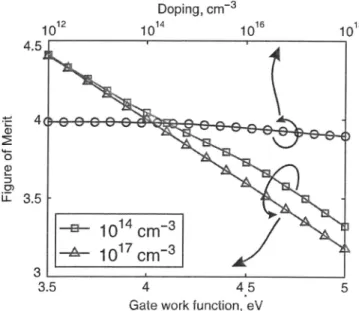
rate. It must be noted that, there is a minimum nano-crystal size for a high-K dielectric, as smaller nanonano-crystals have a higher quantization energy. Smaller nanocrystals observe smaller barriers and high—K dielectrics generally have smaller conduction band barriers on silicon. The figure of merit is also plotted as a function of substrate doping and gate work-function as seen in Figure 9. It is seen that there is a weak dependence on doping den-sity and work—function of the gate. Numerical calculations were used to calculate the band bending for a given set of parameters.
The figure of merit depends strongly on the nanocrystal properties. Smaller nanocrystals can be made with higher areal density but decay faster due to tighter quantum
Doping, cm"3 1012 1014 1016 1018 4.5 .; ' ' Figure of Merit
—A— 1017 cm'3
5
3
.
.
3.5
4
4_5
5
Gate work function, eV
Fig. 9. Figure of merit as a function of gate work-function and substrate doping density for 3 nm diameter nanocrystals, 4 nm tunnel oxide and 20 nm control oxide. Write voltage is 10 V.
1 5 v . r t . Figure Of Merit S U! l nc’ nm
Fig. 10. Figure of merit as a function of nanocrystal diameter, suming
a nanocrystal density of N = lOlzcm‘Z.nc
confinement. The effect of average nanocrystal diameter is plotted in Figure 10, and it is seen that devices with larger and high density nanocrystals perform better.
5. CONCLUSIONS
In this article, we have proposed a charge storage and retention model for NC—MOS memory devices and com-pared it with experimental results. The model envisions storage of carriers in quantized energy levels of NCs. The escape of carriers is modelled by direct tunnelling out of the NCs t0 the substrate. The tunnelling rate depends on the field in the tunnel oxide, which is a function of total number of stored carriers as well as the surface potential of the substrate at a given gate bias. The model can be used to predict the effect of various design parameters such as nanocrystal size and composition, total flat-band voltage shift on write speed and retention time. The model pre-dicts the super-exponential time decay commonly observed in NC—MOS elements. For NC—MOS capacitors contain-ing Ge NCs fabricated by the PECVD technique, NC size related quantum confinement is found to play a role in the storage of charges. The model agrees well with the experimental results, and gives useful insight to NC-MOS memory device design. Theory suggests that high—K dielectric devices with large and dense nano-crystals perform better in terms of retention time and write speed.
Acknowledgments: This work has been partially supported by the European Commission through the FP6 project called SEMINANO under the contract NMP4—CT—2004-505285 and by TUBITAK under contract No 103T115. Thanks are due to Magnus Willander of Goteburg University for supplying the oxidized silicon wafers.
Déna er (1].
References and Notes
1.
S"
S. Tiwuri, F. Rana, H. Hanuli, A. Harlslcin, E. F. Crabbe, and K. Chan, App]. Phys. Let]. 68. 1377 (1996).
X. X. Wang. J. G. Zhang. L. Ding, B. W. Chang, W. K. Ge, J. Z. Yu, and Q. M. Wang, Phys. Rev. B 72, 195313 (2005).
S. Okamoto and Y. Kanemitsu, Phys. Rev. B 54, 1642] (1996). . C. Micsncr, T. Aspcrgcr, K. Brunncr, and G. Abslreilcr. App]. Phys.
L211. 77, 2704 (2000).
J. Xu. Z. H. He, K. Chen, X. Huang, and D. Feng. J. Phys. Com]. Mat. 11, 1631 (1999).
W. K. C1101, V. Ng, S. P. Ng, H. H. Thio, Z. X. Shen. and W. S. Li, J. App]. Phys. 86, 1398 (1999). 7. 8. 10. 11. 12. 13.
A Figure of Merit for Optimization of Nanocrystal Flash Memory Design
T. Z. Lu, M. Alexe. R. Scholz, V. Talelacv. and M. Zacharias, Appl. Phys. L611. 87, 202110 (2005).
A. Gehring and S. Sclberherr. IEEE Trans. Dev. Mat. Re]. 4, 3. 306 (2004).
M. Lenzlinger and E. H. Snow, J. App]. Phys. 40, 278 (1969). A. Nauen, I. Hapkc—Wurst, F. Hohls, U. Zeitler, R. J. Haug, and K. Pierz, Phys. Rev. B 66, 161303(R) (2002).
Y. Nakamura. K. Watanabe, Y. Fukuzawa, and M. lchikawa, Appl.
Phys. Lett. 87, 133119 (2005). “"
M. Dcpas, B. Vcrmcirc, P. W, Mcrtcns. and R. L. Van Mcirhacghc. So]. Stat. Elect. 38, 1465 (1995).
G. D. Wilk, R. M. Wallace, and J. M. Anthony, J. App]. Phys. 89, 5243 (2001).
Received: 11 August 2006. Revised/Accepted: 11 February 2007.