Physica Scripta
PAPER
Electrical characteristics of Au/Ti/n-GaAs contacts
over a wide measurement temperature range
To cite this article: Necmi Biyikli et al 2014 Phys. Scr. 89 095804View the article online for updates and enhancements.
Related content
Capacitance–conductance characteristics of Au/Ti/Al2O3/n-GaAs structures with very thin Al2O3 interfacial layer
A Turut, A Karabulut, K Ejderha et al.
-Influence of Al2O3 barrier on the interfacial electronic structure of Au/Ti/n-GaAs structures
Abdulkerim Karabulut, Hasan Efeoglu and Abdulmecit Turut
-Barrier characteristics of Cd/p-GaTe Schottky diodes based on I--V--T measurements
B Abay, G Çankaya, H S Güder et al.
-Recent citations
Silicon based photodetector with Ru(II) complexes organic interlayer
Abdulkerim Karabulut et al
-The current-voltage characteristics over the measurement temperature of 60-400 K in the Au/Ti/n-GaAs contacts with high dielectric HfO2 interfacial layer
Abdulkerim Karabulut et al
-The electrical and dielectric properties of the Au/Ti/HfO 2 /n-GaAs structures
A. Karabulut et al
Electrical characteristics of Au/Ti/n-GaAs
contacts over a wide measurement
temperature range
Necmi Biyikli
1, Abdulkerim Karabulut
2, Hasan Efeolu
3, Betul Guzeldir
4and
Abdulmecit Turut
51
UNAM Institute of Materials Science and Nanotechnology, Bilkent University, Ankara 06800, Turkey 2Ağrı İbrahim Çeçen University, Faculty of Science and Arts, Department of Physics, Ağrı, Turkey 3
Atatürk University, Faculty of Engineering, Department of Electrical and Electronics Engineering, TR-25240 Erzurum, Turkey
4
Atatürk University, Faculty of Science, Department of Physics, TR-25240 Erzurum, Turkey
5Istanbul Medeniyet University, Faculty of Sciences, Engineering Physics Department, TR-34730 Istanbul, Turkey
E-mail:[email protected]@medeniyet.edu.tr
Received 9 October 2013, revised 15 April 2014 Accepted for publication 16 June 2014
Published 1 August 2014 Abstract
We have fabricated Au/Ti/n-GaAs/In Schottky barrier diodes using the magnetron dc sputter technique. The capacitance–temperature (C–T) measurements with bias voltage as a parameter and the current–voltage (I–V) and capacitance–voltage (C–V) measurements have been made in the temperature range of 60–300 K. The temperature-dependent capacitance measurements have been made at 1.0 MHz. The capacitance versus temperature curve at each bias voltage has four regions with slopes different from each other. The capacitance decreases with a decrease in temperature at each bias voltage. Such a temperature-dependent behavior could be attributed to modulation of the space charge region caused by the emission of deep-level impurities or interface states. The carrier concentration calculated in the−1.0 to −2.0 V range of C−2–V plots was close to the value of 7.43 × 1015cm−3given by the manufacturer around room temperature. The ideality factor value from the I–V characteristics has remained almost unchanged between 1.07 and 1.10 in the temperature range of 150–300 K, indicating that the current across the device obeys the thermionic emission current model quite well over the whole bias range at temperatures above 150 K. Therefore, the conventional Richardson plot in this temperature range has given a Richardson constant of 8.21 A (cm K)−2, within experimental error, which is in very close agreement with the theoretical value of 8.16 A (cm K)−2for n-type GaAs. Again, it has been seen that the ideality factor with the values of 1.10 at 150 K and 1.22 at 60 K does not show a considerable decrease. The experimental parameters show that the Au(90 nm)/Ti(10 nm)/n-GaAs contact is a good candidate for electronic device applications.
Keywords: metal semiconductor contacts, GaAs semiconductor, thermionic emission
(Somefigures may appear in colour only in the online journal)
1. Introduction
Metal–semiconductor (MS) rectifying or ohmic contacts are of great importance for device applications such as organic photovoltaic solar cells, p–n junctions, bipolar transistors,
metal–semiconductor field effect transistors (MESFETs) and high-electron mobility transistors (HEMTs) [1–3]. The MS contact theory serves as the foundation of the physics of semiconductor devices in modern electronic applications and in understanding other semiconductor devices [1–7]. The
| Royal Swedish Academy of Sciences Physica Scripta
refractory metal gate technology has been used for the fab-rication of high-speed MESFETs to reduce the parasitic overlap capacitances between gate and source and series resistance and thus to improve the speed–power performance [5–9]. The occupancy of substrate traps is affected by tem-perature variations, illumination, or irradiation, and this is true of the space charge region. For this reason, the variation of device parameters over a wafer may arise from the nonuni-form distribution of traps in the wafer as well as the interface states [1–7].
Schottky contacts play an important role in controlling the electrical performance of devices. Sehgal et al [10, 11] have investigated the thermal stability of Au/Pt/Ti Schottky contacts on n-GaAs with Ti films of 0–60 nm. They have found [10,11] that by introducing the Tifilm between GaAs and Au/Pt the interdiffusion of Pt and Au is also prevented. These results are useful for reducing the gate metallization resistance of MESFET transistors, and these contacts can next be used to fabricate submicrometer gate length GaAs MES-FETs. Arulkumaran et al [12] have analyzed silicon doped Ti/ n-GaAs Schottky barrier diodes (SBDs) formed by the eva-poration method and obtained a barrier height (BH) of 0.78 eV for these diodes at room temperature. Dio et al [13] have reported forward and reverse current–voltage (I–V) characteristics for Ti/GaAs diodes prepared by ion beam sputtering, and they have shown [13] that the I–V analysis in the temperature range of 100–360 K indicates that the ther-mionic emission (TE) is the main transport mechanism for all the samples, although there are deviations from this behavior at low temperature. They have obtained [13] an average of 0.81 eV for Ti/n-GaAs diodes prepared at different sputtering voltages and currents, and have interpreted the departure from ideal conditions as a direct effect of BH inhomogeneities at the metal–semiconductor interface. Therefore, the perfor-mance of GaAs based devices especially depends on the surface and interface defect density, series resistance, tem-perature and applied bias voltage [1–9].
We have investigated measurement temperature capaci-tance–voltage (C–V) and I–V characteristics of Au/Ti/n-GaAs/In SBDs in the measurement temperature range of 60–300 K. We have fabricated the Au/Ti/n-GaAs/In diodes using the magnetron dc sputter technique. The Au thinfilms have been used as a top layer to protect the Ti metallic layer on the GaAs substrate [14]. As mentioned by Forment et al [15], gallium arsenide is an important semiconductor for optoelectronics, fast computers and microwave applications and Ti/n-GaAs yields a high barrier. As is well known, if the following current in a Schottky barrier obeys the thermionic emission current model quite well in a given temperature range, the experimental conventional Richardson plot of the saturation currents in this temperature range should give an expected Richardson constant (RC) value for the semi-conductor substrate which is in very close agreement with the theoretical value within experimental error. Our purpose is to investigate whether the experimental conventional RC value of the semiconductor substrate used in the fabrication of such a Schottky diode really is in very close agreement with the theoretical RC value or not, and moreover to show
experimentally how the device capacitance under the bias voltage changes with the temperature.
Experimental details
The Au/Ti/n-GaAs SBDs structures were fabricated using an n-type single crystal GaAs wafer with (100) surface orienta-tion, having 400 mm thickness, 2 inch diameter, 7.43 × 1015cm−3carrier concentration and 1.2Ω cm resistiv-ity (given by the manufacturer). Then, the wafer was rinsed in DI water of 18 MΩ cm resistivity for an extended time and dried under N2flow. After surface cleaning of the n-GaAs, high purity (99.999%) indium with a thickness of about 2000Ǻ was coated with at a pressure of about 10−6Torr in a high vacuum system. To form a good ohmic contact, the n-GaAs wafer with the ohmic contact was annealed at 385 °C for 3 min under N2atmosphere. For the Schottky contacts, the n-GaAs wafer was placed on a rotating table. Ti(10 nm) Schottky contacts are made using the magnetron dc sputter technique, and Au(90 nm) was evaporated as a top layer on the Ti/n-GaAs structure to protect the Ti metallic layer in high vacuum system of 10−6Torr. Ti and Au Schottky contacts were squares with 0.01 cm2 area. After the fabrication pro-cess, the I–V characteristics of the Au/Ti/n-GaAs were mea-sured using a Keithley 2400 SourceMeter. All measurements were made in the temperature range of 60–300 K using a temperature controlled Janis vpf-475 cryostat, which enables us to make measurements in the temperature range of 20–450 K. The sample temperature was always monitored by use of a copper–constantan thermocouple close to the sample and measured with a Keithley model 199 DMM scanner and Lakeshore model 321 auto-tuning temperature controller with sensitivity better than ±0.1 K.
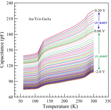
Figure 1.Experimental capacitance plots as a function of the temperature with bias voltage as a parameter at 1.0 MHz.
2
2. Results and discussion
Figure 1 shows the experimental capacitance versus tem-perature curves for the Au/Ti/n-GaAs SBD, where the capa-citance is a function of the measurement temperature with the bias voltage as a parameter at 1.0 MHz. The capacitance decreases with a decrease in temperature at each voltage. It can be seen from figure 1 that there are four regions with different slopes from 60 to 300 K at each bias voltage. It can be said that the deep level or interface states with different densities and energies affect each region. The slopes decrease with bias voltage decreasing from +0.20 to −2.0 V. That is, the slopes at −2.0 V are lower than those at +0.20 V, depending on the measurement temperature. Such a tem-perature-dependent behavior of the capacitance could be attributed to modulation of the space charge region caused by the emission of more carriers from the required levels such as deep-level impurities or interface states [2, 3, 16]. As is known, the capacitance value decreases or approaches the space charge capacitance because the interface states or deep levels cannot follow the ac signal at sufficiently high fre-quencies [2,3,16–19].
As is well known, a C–V plot in the idealized case should show an increase in capacitance with increasing forward voltage independent of temperature and frequency. However, the experimental results had shown that the capacitance in the C–V plot might be influenced by the nonidealities [2,3,17–23]. Figure2 shows the C–V characteristics of the Au/Ti/n-GaAs SBD at 1.0 MHz in the temperature range of 60–300 K with steps of 10 K. The C–V characteristics were measured in +0.20 to−2.0 V range at each temperature, where the forward bias branch ranges from 0.00 to 0.20 V, and the reverse bias branch ranges from 0.00 to −2.0 V. As can be seen fromfigure2, the decrease in capacitance in the reverse
bias from 0.00 to −2.00 V implies an increase in the semi-conductor depletion width. Since the charge neutrality con-dition at the interface should be satisfied, widening of the depletion width in the reverse bias C–V characteristics results from a reduction of the ionized donor concentration.
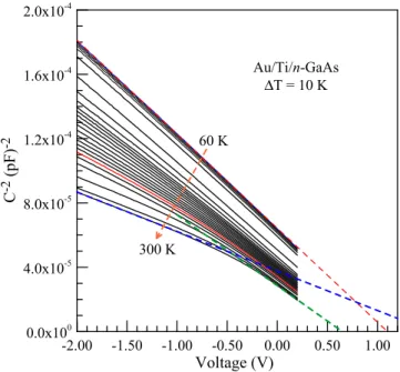
Figure 3 shows the reverse and forward bias C−2–V curves from the data in the temperature range of 60–300 K in figure2. The C−2–V curves show two linear regions separated by a transition segment, especially from 300 to 130 K. That is, the curves have two slopes in the temperature range of 130–300 K and then trend approximately to have a single slope over the whole voltage range with decreasing tem-perature. The constant slope yields a uniform doping con-centration. This behavior may be due to a change of the carrier concentration profile depending on the sample tem-perature. The straight line intercepts of the C−2–V plots with the voltage axis were obtained from both linear regions at each temperature. The C–V BH and carrier concentration values are determined from intercepts and slopes of the straight lines in the C−2–V plots for each temperature. These values are given infigures 3and 4.
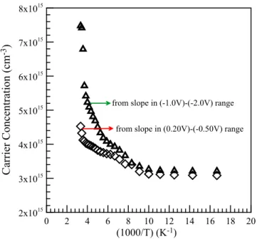
Figure4shows the carrier concentrations calculated from the two present slopes at each temperature infigure2. As seen from figure4, the difference between the carrier concentra-tions for the two regions decreases with decreasing tem-perature. It can be said that the carrier concentration has almost the same value from 60 to 120 K. For example, the carrier concentration is 3.21 × 10¹⁵ and 3.10 × 1015cm−3 at 60 K while it is 7.48 × 10¹⁵and 4.53 × 1015cm−3at 300 K for the two mentioned regions in figure3. Furthermore, the car-rier concentration decreases with a decrease in temperature because more electrons may be frozen at the required state levels in the freeze-out region, and it remains almost constant from 60 to 120 K. Moreover, the value of 7.48 × 1015cm−3
Figure 2.Capacitance–voltage curves for the Au/Ti/n-GaAs structure at 1.0 MHz in the temperature range of 60–300 K.
Figure 3.C−2–V plots for the Au/Ti/n-GaAs structure at 1.0 MHz in the temperature range of 60–300 K.
from the slope in the−1.0 to −2.0 V range at 300 K is in close agreement with the value of 7.43 × 1015cm−3 given by the manufacturer. Thus, when these values and figure 3 are considered, it can be said that the slope in the −1.0–0.0 V range becomes more pronounced with increasing temperature. That is, it can be said that the bulk deep levels or interface states are more effective and they lead to reduction of the carrier concentration in about the −1.0–0.0 V range at each temperature above 120 K. In addition to these, it was found by Vandenbroucke [22] that a large density of donor-like defects for the diodes with a sputter-deposited metal contact is present in the near-surface region, together with a region of decreasing density deeper into the semiconductor. These donor-like states in the surface region, induced during bom-bardment of the substrate, are believed to be responsible for the observed electrical behavior [3]. The carrier concentration remains almost constant as the temperature is decreased from 60 to 120 K. More electrons may be frozen at the donor level in the freeze-out region.
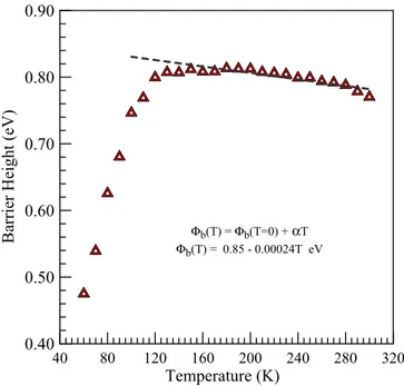
As mentioned above, figure5 shows the obtained C–V BH values (open triangles) from the C−2–V plots for each temperature. The BH value has linearly increased from 0.81 eV at 300 K to 0.89 eV at 120 K, and has deviated from linearity at temperatures below 120 K. The temperature coefficient of the BH can be determined from this plot. The temperature dependence of the BH is expressed as
Φ( )T = Φ(T=0) −αT. According to the equation, the slope of the straight line yields a value ofα = −0.54 meV K−1, called the temperature coefficient value of the BH. Passler [23], Thurmond [24] and Lautenschlager et al [25] indicated the values of −0.472, −0.5405 and −0.55 meV K−1 for the temperature coefficient of the energy band gap of n-type GaAs, respectively. The variation of the BH value with temperature is normally explained within the frame of the
Fermi level pinning concept due to the temperature dependent variation in the band gap [24,25]. The temperature coefficient of the BH obtained by us is approximately equal to the temperature coefficient of the energy gap of n-type GaAs.
Figure 4.Carrier concentration plots obtained from two regions for the Au/Ti/n-GaAs structure in the temperature range of 60–300 K.
Figure 5.BH versus temperature plot for the Au/Ti/n-GaAs Schottky barrier diode: open triangles, the BH values in the 0.00 to−0.80 V range of the C−2–V curves at each temperature; open squares, the BH values from the Norde plot (figure10) plotted using the forward bias I–V data in figure6. The dashed lines arefits to the experi-mental data.
Figure 6.Current–voltage curves for the Au/Ti/n-GaAs structure in the temperature range of 60–300 K.
4
Figure 6 shows the semi-log current–voltage curves of the Au/Ti/n-GaAs Schottky barrier diode in the temperature range of 60–300 K. The experimental values of the ideality factor and SBH have been calculated from the intercept and slope of the linear portion of the forward-bias ln I–V plot at each temperature infigure6. The intercept of the linear por-tion corresponds to the saturapor-tion current at V = 0 volts. Figure 7 shows the SBH versus measurement temperature plot for the device in the temperature range of 60–300 K. The SBH value has increased from 0.77 eV at 300 K to 0.81 eV at 180 K with a slope of −0.24 mV K−1, and has remained almost at the same value as 0.81 eV in the 130–180 K range. The dashed straight line infigure7shows afit to experimental data in the 130–300 K range. Again, the BH value has sharply decreased from 0.82 eV at 130 K to 0.48 eV at 60 K. The decrease of the BH in the 60–130 K range is in very close agreement with the results obtained in [26–29]. It has been mentioned in [26] that the BH is not temperature dependent but rather the current transport mechanisms. In fact, the cur-rent processes are temperature dependent and consequently the extraction of the BH indicates that the BH changes with temperature [26]. When varying the temperature different current mechanism changes too [26].
The ideality factor value of the device has remained almost unchanged between 1.07 and 1.10 in the temperature range of 150–300 K, and has decreased from 1.10 at 150 K to 1.22 at 60 K. These values are given in table1. Göksu et al [9] obtained the BH and ideality factor values of 0.62 and 1.61 (at 60 K) and 0.91 and 1.02 (at 320 K) for Ti/n-GaAs SBDs without an Au layer prepared by magnetron DC sput-tering, respectively. Arulkumaran et al [12] have obtained a BH of 0.78 eV at room temperature for Ti/n-GaAs SBDs formed by the evaporation method. Dio et al [13] have
obtained an average of 0.81 eV for Ti/n-GaAs diodes pre-pared at different sputtering voltages and currents. The values of the ideality factor near unity indicate that the experimental I–V data obey the TE current model quite well over the whole
Figure 7.Barrier height versus measurement temperature plot for Au/Ti/n-GaAs structure in the temperature range of 60–300 K. The dashed straight line shows afit to experimental data in the 130–300 K range.
Table 1.The diode parameters from forward bias I–V characteristics: Φb, barrier height; n, ideality factor; I0, saturation current.
Temperature (K) Φb(eV) n I0 300 0.770 1.074 6.81 × 10⁻¹⁰ 290 0.779 1.063 1.64 × 10⁻¹⁰ 280 0.788 1.059 3.40 × 10⁻¹¹ 270 0.792 1.042 8.00 × 10⁻¹² 260 0.794 1.052 1.84 × 10⁻¹² 250 0.799 1.054 3.20 × 10⁻¹³ 240 0.799 1.050 6.40 × 10⁻¹⁴ 230 0.804 1.048 8.44 × 10⁻¹⁵ 220 0.806 1.049 1.1 × 10⁻¹⁵ 210 0.808 1.058 1.22 × 10⁻¹⁶ 200 0.812 1.052 9.00 × 10⁻¹⁸ 190 0.813 1.061 6.81 × 10⁻¹⁹ 180 0.813 1.074 3.70 × 10⁻²⁰ 170 0.808 1.077 2.10 × 10⁻²¹ 160 0.808 1.098 6.10 × 10⁻²³ 150 0.812 1.104 8.2 × 10⁻²⁵ 140 0.807 1.130 1.20 × 10⁻²⁶ 130 0.807 1.183 5.80 × 10⁻²⁹ 120 0.800 1.150 2.60 × 10⁻³¹ 110 0.769 1.230 5.00 × 10⁻³³ 100 0.746 1.280 1.7 × 10⁻³⁵ 90 0.680 1.438 4.51 × 10−36 80 0.626 1.601 1.73 × 10−37 70 0.539 1.926 5.10 × 10−37 60 0.475 2.221 3.30 × 1038
Figure 8.nT versus T plot showing the T0anomaly for the Au/Ti/n-GaAs structure in the temperature range of 60–300 K. The solid line is ideal Schottky diode behavior given as ideality factor n = 1; the dashed straight line shows afit to experimental data.
bias range at temperatures above 150 K. The values of the SBH and ideality factor have been calculated using equation (1) and (2), called the TE current relationships, given in [1–3]. The case can be seen more clearly infigure8, which shows the nT versus T plot for Au/Ti/n-GaAs in the tem-perature range of 60–300 K. This is called the T0anomaly plot determining the temperature dependence of the ideality factor n. The solid line infigure8is ideal Schottky diode behavior given as n = 1, which goes through the origin. The dashed straight linefitted to experimental data for information about the T0effect should be parallel to the ideal Schottky line. A value of T0= 11.28 K was obtained from the experimental plot. As can be seen fromfigure8, the dashed straight line significantly deviates from linearity below 120 or 130 K. It has been pointed out in [27–33] that the change at low tem-peratures may be ascribed to the currentflow through small regions, so-called‘patches’, with low BH. The conventional Richardson ln(I0/T2) versus (kT)−1 plot in the temperature range of 60–300 K in figure 9 is linear in the 120–300 K range, where I0 is the saturation current in the TE current expression [1–3]. Therefore, it has given an RC of 8.21 A (cm K)−2 from the conventional Richardson plot (figure 9), within experimental error. This value is in very close agree-ment with the theoretical value of 8.16 A (cm K)−2for n-type GaAs. Thus, it can be said that the I–V characteristics of the device obey the TE current model in the 120–300 K range [34–41].
As is well known, when the MS Schottky diodes are characterized by I–V and C–V data, the BH calculated from the C–V data is higher than the BH value extracted from the saturation current of the semi-log forward bias characteristics and gives an average value of the BHs of the patches present in the Schottky contact. The mentioned saturation current is the intercept of the linear portion of the semi-log forward bias
curve. Osvald [33] says that the I–V and C–V measurement techniques are differently sensitive to possible occurrence in the inhomogeneous Schottky contacts at especially low tem-peratures. Because the current of the Schottky diode depends exponentially on the BH, the inhomogeneities and small patches with lower BH in the contact strongly influence the resulting apparent BH [28–41].
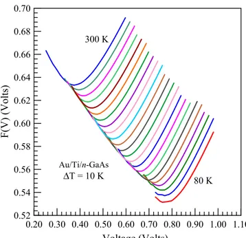
The BH of the Au/Ti/n-GaAs/In can be also calculated by Norde’s method [42], because the device shows an ideal behavior. A function F(V) was derived from the TE current expression by Norde [40]: γ = − * ⎜ ⎟ ⎛ ⎝ ⎞ ⎠ F V V kT q I V AA T ( ) ln ( )2 , (1)
where the current I V( ) is obtained from the I–V curves at each temperature in figure 6. This function can be used to determine the BH [42]. Figure10 shows theF V( ) versus V plots obtained using the experimental I–V data in equation (1). The BH relation is given as follows [38]:
Φ T =F V
(
)
+ V − kT q ( ) 2 , (2) min minwhere F V
(
min)
is the minimum value of F V( )and the cor-responding voltage and current are Vminand Imin, respectively. The BH values from the F(V)–V curves are given as a func-tion of temperature in figure4 (indicated by open squares). The expressions (1) and (2), which are called Norde’s func-tions, are based on the TE current mechanism [2,3,42,43]. The BH value has linearly increased from 0.81 eV at 300 K to 0.89 eV at 120 K, and deviates from linearity at temperatures below 120 K. As can be seen from figure5, the BH values calculated by Norde’s method and C−2–V characteristics coincide with each other in the temperature range of 120–300 K, but not at low temperatures below 120 K. AsFigure 9.Conventional Richardson plot for the Au/Ti/n-GaAs
structure in the temperature range of 60–300 K. Figure 10.in the temperature range of 60–300 K.Norde plot for the Au/Ti/n-GaAs Schottky barrier diode
6
indicated above, the BH values calculated from the C–V data give an average value of the BHs of patches present in the Schottky contact. Thus, it can be said that Norde’s method used to calculate the BH value in the ideal Schottky diodes gives approximately an average value of the BHs at each temperatures except for low temperatures [28, 42, 43]. The temperature coefficient of the BH can be also determined from this plot. The fitting to the Φ(T) data equation above yields a straight line with the slope of α = −0.51 meV K−1 called the temperature coefficient value of the BH. Thus, this result has been also confirmed by the temperature coefficient value (open triangles) of α = −0.54 meV K−1 from C−2–V curves infigure4.
In conclusion, the I–V characteristics of the device have almost given the diode parameters independent of the mea-surement temperature at temperatures above 130 K. It can be said that the Au/Ti/n-GaAs/In diodes fabricated by the mag-netron DC sputter technique are a candidate for electronic device applications. The BH value from the I–V data of the device has increased from 0.77 eV at 300 K to 0.82 eV at 180 K, and has remained at almost the same value in the 130–180 K range. Furthermore, it has been found that the experimental conventional RC value of the semiconductor substrate used in the fabrication of the Schottky diode is really in very close agreement with the theoretical RC value, because the I–V characteristics of the device obey the TE current mechanism in the 120–300 K range. The capacitance versus temperature curves plotted as a function of the bias voltage characteristics have given four regions with different slopes at each bias voltage, and the slopes decrease with decreasing voltage from 0.20 to −2.0 V. A carrier con-centration value of 7.43 × 1015cm−3was calculated from the C−2–V plots around room temperature, which is close to the value given by the manufacturer.
Acknowledgements
This work was supported by Ataturk University (Project No: BAP 2011/365). The samples were prepared at Bilkent Uni-versity UNAM. The authors wish to thank Ataturk UniUni-versity and Bilikent University UNAM.
References
[1] Saghrouni H, Hannachi R, Jomni S and Beji L 2013 Physica B
422 64–71
[2] Rhoderick E H and Williams R H 1988 Metal–Semiconductor Contacts 2nd edn (Oxford: Clarendon)
[3] Sze S M 1981 Physics of Semiconductor Devices 2nd edn (New York: Wiley)
[4] Lajn A, von Wenckstern H, Grundmann M, Wagner G, Barquinha P, Fortunato E and Martin R 2013 J. Appl. Phys.
113 044511
[5] Korucu D and Duman S 2013 Thin Solid Films531 436–41 [6] Jyothi I, Seo M-W, Janardhanam V, Shim K-H, Lee Y-B,
Ahn K-S and Choi C-J 2013 J Alloys and Comp.556 252–8
[7] Ahaitouf A, Srour H, Hamady S O S, Fressengeas N, Ougazzaden A and Salvestrini J P 2012 Thin Solid Films
522 345–51
[8] Ozavcı E, Demirezen S, Aydemir U and Altındal S 2013 Sensors and Actuators A194 259
[9] Goksu T, Yıldırım N, Korkut H, Ozdemir A F, Turut A and Kokce A 2010 Microelect. Engineer87 1781
[10] Sehgal B K, Gulati R, Naik A A, Vinayak S, Rawal D S and Sharma H S 1997 Mater. Sci. Engineer. B48 229 [11] Sehgal B K, Bhattacharya B, Vinayak S and Gulati R 1998
Thin Solid Films330 146
[12] Arulkumaran S, Arokiaraj J, Dharmarasu N and Kumar J 1996 Nucl. Inst. Meth. Phys. Res. B119 519
[13] Di Dio M, Cola A, Lupo M G and Vasanelli L 1995 Solid-State Electron.38 1923
[14] Gao W, Li Z and Sammes N 2011 An Introduction to Electronic Materials for Engineers 2nd edn (Singapore: World Scientific)
[15] Forment S, Biber M, Van Meirhaeghe R L, Leroy W P and Türüt A 2004 Semicond. Sci. Technol.19 1391
[16] Janardhanam V, Kumar A A, Reddy V R and Reddy P N 2009 J. Alloys Comp.485 467
[17] Khuchua N P, Khvedelidze L V, Tigishvili M G, Gorev N B, Privalov E N and Kodzhespirova I F 2003 Russian Microelectronics32 257–74
[18] Lakshmi B P, Reddy M S P, Kumar A A and Reddy V R 2012 Curr. Appl. Phys.12 765
[19] Turut A, Yalcin N and Saglam M 1992 Solid State Electron.35
835–41
[20] Kundu S, Kumar A, Banerjee S and Banerji P 2012 Mater. Sci. Semicond. Process.15 386
[21] Saglam M and Turut A 1997 Semicond. Sci. Technol.12
1028–31
[22] Vandenbroucke D A, Van Meirhaeghe R L, Laflere W H and Cardon F Semicond. Sci. Technol.2 293–8
[23] Passler R 2002 Phys. Rev. B66 085201
[24] Thurmond C D 1975 J. Electrochem. Soc.122 1133 [25] Lautenschlager P, Garriga M, Logothetidis S and Cardona M
1987 Phys. Rev. B35 9174
[26] Donoval D, Barus M and Zdimal M 1991 Solid State Electronics34 1365–73
[27] Zhu S Y, Detavernier C, Van Meirhaeghe R L, Cardon F, Ru G-P, Qu X-P and Li B-Z 2000 Solid-State Electron.
44 1807
[28] Korucu D, Turut A and Efeoglu H 2013 Physica B414 35–41 [29] Gammon P M et al 2013 J. Appl. Phys.114 223704 [30] Chand S, Kaushal P and Osvald J 2013 Mater. Sci. Semicon.
Process.16 454–60
[31] Tung R T 2014 Appl. Phys. Rev.1 011304
[32] Sullivan J P, Tung R T, Pinto M R and Graham W R 1991 J. Appl. Phys.70 7403
[33] Osvald J 1999 J Apll. Phys.85 1935
[34] Tunç T, AltindalŞ, Uslu İ, Dökme İ and Uslu H 2011 Mater Sci. Semicon. Process.14 139
[35] Osvald J and Horvath Z J 2004 Appl. Surf. Sci.234 349–54 [36] Huang W-C, Lin T-C, Horng C-T, Li Y-H and Sci M 2013
Semicon. Process.16 418
[37] Tuğluoğlu N, Yüksel Ö F, Karadeniz S and Şafak H 2013 Mater. Sci. Semicon. Process.16 786
[38] Yildirim N, Dogan H, Korkut H and Turut A 2009 Int. J. Modern Phys. B23 5237–49
[39] Kaushal P, Chand S and Osvald J 2013 Int. J. Electronics100
686–98
[40] Tataroğlu A and Pür F Z 2013 Phys. Scr.88 015801
[41] Yildirim N, Korkut H and Turut A 2009 Eur. Phys. J. Appl. Phys.45 10302
[42] Norde H 1979 J. Appl. Phys.50 5052
[43] Korkut H, Yildirim N and Turut A 2009 Microelect. Engineer