© 2008 WILEY-VCH Verlag GmbH & Co. KGaA, Weinheim
p s s
current topics in solid state physics
c
status
solidi
www.pss-c.com
physica
Carrier-induced refractive index
change in InN
C. Bulutay1,*and N. A. Zakhleniuk2
1Department of Physics and Institute of Materials Science and Nanotechnology, Bilkent University, Ankara 06800, Turkey 2Department of Computing and Electronic Systems, University of Essex, Wivenhoe Park, Colchester, CO4 3SQ, UK
Received 2 July 2007, revised 5 November 2007, accepted 6 November 2007 Published online 18 December 2007
PACS 78.20.Ci, 78.30.Fs
∗Corresponding author: e-mail [email protected], Phone: +90-312-2902511, Fax: +90-312-2664579
Rapid development of InN technology demands compre-hensive assessment of the electronic and optoelectronic potential of this material. In this theoretical work the effect of free electrons on the optical properties of the wurtzite phase of InN is investigated. The blue shift of the optical absorption edge by the free-carrier band fill-ing is known as the Burstein-Moss effect for which InN offers to be a very suitable candidate as has been re-cently demonstrated experimentally. Due to well known Kramers-Kronig relations, a change in absorption is
accompanied by a change in the index of refraction. Con-sidering n-type InN samples with free electron
concen-trations ranging from5×1017to5×1020cm−3, and
em-ploying a nonlocal empirical pseudopotential band struc-ture, it is shown that this leads to a few percent change of the index of refraction. These carrier-induced refrac-tive index changes can be utilized in optical switches, futhermore it needs to be taken into account in the de-sign of InN-based optical devices such as lasers and op-tical modulators.
1 Introduction The optoelectronic applications of InN are of particular interest since the InGaN alloys are capable to cover wide range of optical spectra from blue-green to near-infrared region [1]. A common property of the grown InN films is the very high unintentional electron density that ranges from1018to mid-1020cm−3[2–4]. As a direct consequence it has been shown experimentally that this gives rise to a blue shift of the optical absorption edge [5, 6]. This is known as the Burstein-Moss effect which is the increase of the effective band-gap due to Pauli blocking of the optical transitions to the filled portions of the bands. As a consequence, the high electron concentration in n-type InN samples leads to the reduction of the absorption which is described by the imaginary part of the dielectric func-tion. According to the Kramers-Kronig relation (KKR), the real part of the dielectric function is intimately connected to its imaginary part. Hence, the refractive index of a semi-conductor can be modulated by the free carriers [7]. Sev-eral types of semiconductor optical devices utilize this ef-fect, like digital switches, phase modulators, tunable Bragg gratings in distributed Bragg reflector lasers [8].
The carrier-induced refractive index change is most pro-nounced in semiconductors with small effective masses and energy gaps, like n-InSb [7]. With the revised narrow band gap of InN [2], in this theoretical work we show that this carrier-induced refractive index change is particularly im-portant for InN. As we shall show below, this is due to in-teresting conduction band structure where the band filling gives rise to much larger absorption band edge shifts.
2 Theoretical results For a realistic assessment, we employ a nonlocal empirical pseudopotential band struc-ture of InN that reproduces the most up-to-date band data such as the effective masses and band nonparabolicities [9]. The corresponding density of states is shown in Fig. 1. It can be observed that due to the narrow band-gap nature of this material the low density of states prolongs to about 2 eV from the conduction band edge. This causes substan-tial band filling effects as illustrated in Fig. 2 which dis-plays theshift in the absorption edge, known as the Burstein-Moss effect. As a word of caution, we should note that this shift is to some extend overestimated compared to the ex-perimentally observed value [6]. This is possibly due to
© 2008 WILEY-VCH Verlag GmbH & Co. KGaA, Weinheim
512 C. Bulutay and N. A. Zahkleniuk: Carrier-induced refractive index change in InN
© 2008 WILEY-VCH Verlag GmbH & Co. KGaA, Weinheim www.pss-c.com
accompanied red shift resulting from the band-gap renor-malization [10] which is not included in this work.
Figure 1 Computed density of states of InN; energy reference is
set to valence band maximum.
Figure 2 The shift of the absorption edge due to conduction band
filling by excess electrons.
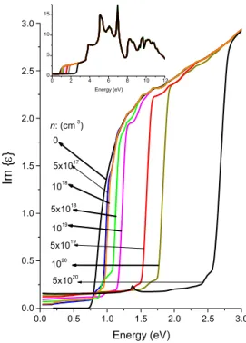
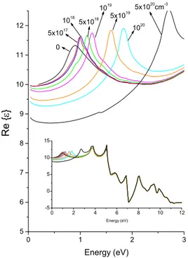
The direct consequence of this carrier-induced blue shift of the effective optical gap is the modification of the ab-sorption profile which is described by the imaginary part of the dielectric function, as shown in Fig. 3. On the other hand, as a manifestation of the causality principle, the KKR links the imaginary and real parts of the dielectric func-tion. In Fig. 4 we show the associated modification of the real part of the dielectric function due to excess electrons in InN. Both dielectric functions in Figs. 3 and 4 refer to
Figure 3 Imaginary part of the in-plane (perpendicular to c-axis)
dielectric function for different excess electron densities. The in-set shows the behaviour for a broader energy range.
the photon polarization perpendicular to thec-axis of the wurtzite crystal.
Finally, we display in Fig. 5 the dependence of the static refractive index on the excess electron density. It can be observed that this gives rise to up to few percent carrier-induced tunability of the refractive index. Already at a car-rier density of a few1018cm−3the predicted refractive in-dex change reaches the level of 10−2which is substantially larger than the index change produced by the Pockels or Franz-Keldysh effects under significant applied fields [7]. Undoubtedly, this is a valuable feature for optical device applications such as optical switches, phase modulators and tunable Bragg gratings in Distributed Bragg Reflector lasers.
3 Conclusion In this theoretical work, we investi-gate the Burstein-Moss effect in n-type InN based on the nonlocal empricial pseudopotential band structure. We ob-serve substantial blue-shift of the absorption edge for the typical grown InN samples with unintentional free elec-tron densities on the order of 1019 cm−3. By obtaining the full energy dependence of the imaginary part of the dielectric function, its real part is also calculated through the KKR. As a result, a free carrier-induced refractive in-dex change by few percents is demonstrated. This suggests possible InN-based optical device applications such as in the optical switches, phase modulators and tunable Bragg gratings in distributed Bragg reflector lasers. However, it
www.pss-c.com © 2008 WILEY-VCH Verlag GmbH & Co. KGaA, Weinheim Original
Paper
Figure 4 Real part of the in-plane (perpendicular to c-axis)
di-electric function for different excess electron densities. The inset shows the behaviour for a broader energy range.
Figure 5 The percentage change of the index of refraction versus
excess electron density.
should be noted that we do not include the band gap renor-malization which leads to a red shift of the optical gap as the carrier density increases; this becomes quite significant at1019 cm−3and beyond [10] which can partially cancel the Burstein-Moss blue shift. Similarly, the free carrier
ab-sorption is not taken into account. Our primary goal here was to demonstrate the importance of the full-band calcu-lations of the optical parameters of InN.
Acknowledgements The authors would like to thank the
British Council for supporting the partnership of the Bilkent and Essex universities. The work of C.B. is also supported by the Turkish Scientific and Technical Council T ¨UB˙ITAK within the COST 288 Action.
References
[1]J. Wu, W. Walukiewicz, K. M. Yu, W. Shan, J. W. Ager, E. E. Haller, H. Lu, W. J. Schaff, W K. Metzger, and S. Kurtz, J. Appl. Phys.94, 6477 (2003).
[2]J. Wu, W. Walukiewicz, K. M. Yu, J. W. Ager III, E. E. Haller, H. Lu, W. J. Schaff, Y. Saito, and Y. Nanishi, Appl. Phys. Lett.80, 3967 (2002).
[3]V. Yu. Davydov, A. Klochikhin, V. V. Emtsev, S. V. Ivanov, V. V. Vekshin, F. Bechstedt, J. Furthm¨uller, H. Harima, A. V. Mudryi A. Hashimoto, A. Yamamoto, J. Aderhold, J. Graul, and E. E. Haller, phys. stat. sol. (b)230, R4 (2002).
[4]Y. Nanishi, Y. Saito, and T. Yamaguchi, Jpn. J. Appl. Phys. 42, 2549 (2003).
[5]A. G. Bhuiyan, K. Sugita, K. Kasahima, A. Hashimoto, A. Yamamoto, and V. Y. Davydov, Appl. Phys. Lett.83, 4788 (2003).
[6]J. Wu, W. Walukiewicz, S. X. Li R. Armitage, J. C. Ho, E. R. Weber, E. E. Haller, H. Lu, W. J. Schaff, A. Barcz, and R. Jakiela, Appl. Phys. Lett.84, 2805 (2004).
[7]B. R. Bennett, R. A. Soref, and J. A. Del Alamo, IEEE J. Quantum Electron.26, 113 (1990).
[8]J. -P. Weber, IEEE J. Quantum Electron.30, 1801 (1994), and references therein.
[9]C. Bulutay and B. K. Ridley, Superlattices Microstruct.36, 465 (2004).
[10]J. Wu, W. Walukiewicz, W. Shan, K. M. Yu, J. W. Ager, E. E. Haller, H. Lu, and W. J. Schaff, Phys. Rev. B66, 201403 (2002).