First-principles study of zinc oxide honeycomb structures
M. Topsakal,1 S. Cahangirov,1E. Bekaroglu,1 and S. Ciraci1,21UNAM-Institute of Materials Science and Nanotechnology, Bilkent University, Ankara 06800, Turkey 2Department of Physics, Bilkent University, Ankara 06800, Turkey
共Received 12 March 2009; published 11 December 2009兲
We present a first-principles study of the atomic, electronic, and magnetic properties of two-dimensional 共2D兲, single and bilayer ZnO in honeycomb structure and its armchair and zigzag nanoribbons. In order to reveal the dimensionality effects, our study includes also bulk ZnO in wurtzite, zincblende, and hexagonal structures. The stability of 2D ZnO, its nanoribbons and flakes are analyzed by phonon frequency, as well as by finite temperature ab initio molecular-dynamics calculations. 2D ZnO in honeycomb structure and its armchair nanoribbons are nonmagnetic semiconductors but acquire net magnetic moment upon the creation of zinc-vacancy defect. Zigzag ZnO nanoribbons are ferromagnetic metals with spins localized at the oxygen atoms at the edges and have high spin polarization at the Fermi level. However, they change to nonmagnetic metal upon termination of their edges with hydrogen atoms. From the phonon calculations, the fourth acous-tical mode specified as twisting mode is also revealed for armchair nanoribbon. Under tensile stress the nanoribbons are deformed elastically maintaining honeycomblike structure but yield at high strains. Beyond yielding point honeycomblike structure undergo a structural change and deform plastically by forming large polygons. The variation in the electronic and magnetic properties of these nanoribbons have been examined under strain. It appears that plastically deformed nanoribbons may offer a new class of materials with diverse properties.
DOI:10.1103/PhysRevB.80.235119 PACS number共s兲: 73.22.⫺f, 75.75.⫹a, 63.22.⫺m
I. INTRODUCTION
Graphene, a monolayer layer of carbon atoms in honey-comb structure, is offering exceptional properties1–3 which
may lead to important applications in various fields. Nor-mally, two-dimensional 共2D兲 graphene is semimetallic and its electrons and holes behave like a massless Dirac fermion. Whereas 2D boron nitride 共BN兲,4 Group III-V analog of
graphene, in ionic honeycomb structure is a wide band-gap semiconductor. Unusual properties of graphene and BN na-noribbons have been revealed extensively in recent papers.5–11 More recently, based on state-of-the-art first-principles calculations it was predicted that Si and Ge,12even
binary compounds of Group IV elements and III-V compounds13 can form 2D stable monolayer honeycomb
structures. Earlier studies on ZnO and its nanowires gave first indications that graphitic ZnO can exists.14,15 Very thin
nanosheets,16 nanobelts,17 nanotubes,18 and nanowires19 of
ZnO have already been synthesized. Two-monolayer-thick ZnO共0001兲 films grown on Ag共111兲 were reported.20
Because of its wide band gap of ⬃3.3 eV and large ex-citon binding energy of 60 meV leading to vast optoelec-tronic applications including light-emitting diodes and solar cells,21,22ZnO has been the subject of various researches. It
was reported that the vacancy defects can be intentionally created by electron-irradiation method.23It has been also re-ported that Zn vacancy induces ferromagnetism in ZnO thin films and nanowires without any need of doping with transition-metal atoms.24 These magnetic properties might
provide superior advantages in biomedical applications be-cause of nontoxic nature of ZnO as opposed to transition-metal ions.
In this paper a comprehensive study of the atomic, elec-tronic, and magnetic properties of monolayer, bilayer, and
nanoribbons of II-VI ionic ZnO compound in honeycomb structures are carried out using first-principles calculations. In order to reveal the dimensionality effects, we started with the energetics and electronic energy bands of ZnO in differ-ent three-dimensional 共3D兲 bulk crystalline structures and compared them with those of 2D ZnO honeycomb structure. Our analysis based on phonon dispersions and finite-temperature ab initio molecular-dynamics calculations pro-vides evidence for the stability of free-standing 2D mono-layer, bilayer, and quasi-one-dimensional 共quasi-1D兲 nanoribbons of ZnO honeycomb structures. These structures can be in different local minima on the Born-Oppenheimer surface, in spite of the fact that they are not synthesized yet. We found that 2D monolayer and bilayer ZnO are nonmag-netic semiconductors but attain magnonmag-netic properties upon creation of Zn-vacancy defect. ZnO nanoribbons exhibit in-teresting electronic and magnetic properties depending on their orientation. While armchair ZnO nanoribbons are non-magnetic semiconductors with band gaps varying with their widths, bare zigzag nanoribbons are ferromagnetic metals. These electronic and magnetic properties show dramatic changes under elastic and plastic deformation. Hence, ZnO nanoribbons can be functionalized by plastic deformation. Results obtained in this study indicates that 2D monolayer and bilayer ZnO honeycomb structures and quasi-1D arm-chair and zigzag nanoribbons display unusual electronic, magnetic, and mechanical properties, which hold the promise of interesting technological applications.
II. MODEL AND METHODOLOGY
We have performed first-principles plane-wave calcula-tions within density-functional theory共DFT兲 using projector augmented wave potentials.25 The exchange-correlation
po-tential has been approximated by generalized gradient ap-proximation 共GGA兲 using PW91 共Ref. 26兲 functional both
for spin-polarized and spin-unpolarized cases. Recently, spin-polarized calculations within DFT have been used suc-cessfully to investigate magnetic properties of vacancy de-fects in 2D honeycomb structures. Also interesting spintronic properties of nanoribbons have been revealed using spin-polarized DFT.6The success of spin-polarized DFT
calcula-tions has been discussed in Ref.27.
All structures have been treated within supercell geometry using the periodic boundary conditions. A plane-wave-basis set with kinetic-energy cutoff of 500 eV has been used. The interaction between ZnO monolayers in adjacent supercells is examined as a function of their spacing. Since the total energy per cell has changed less than 1 meV upon increasing the spacing from 10 to 15 Å, we used the spacing of⬃10 Å in the calculations. In the self-consistent potential and total-energy calculations the Brillouin zone 共BZ兲 is sampled by, respectively, 共15⫻15⫻15兲, 共25⫻25⫻1兲, and 共25⫻1⫻1兲 special k points for 3D bulk, 2D honeycomb, and 1D 共nan-oribbons兲 ZnO. This sampling is scaled according to the size of superlattices. For example, BZ was sampled by 共3⫻3 ⫻1兲 special k points for defect calculations using 共7⫻7兲 supercell of 2D ZnO honeycomb structure. All atomic posi-tions and lattice constants are optimized by using the conju-gate gradient method, where the total energy and atomic forces are minimized. The convergence for energy is chosen as 10−5 eV between two steps and the maximum Hellmann-Feynman forces acting on each atom is less than 0.02 eV/Å upon ionic relaxation. The pseudopotentials having 12 and 6 valence electrons for the Zn 共Zn:4s23d10兲 and O ions 共O:2s22p4兲 are used. Numerical plane-wave calculations are performed by using VASP package.28,29 While all numerical
calculations of structure optimization, electronic energy, and phonon dispersions are carried out within GGA using
VASP,28,29some of the calculations are checked also by using
PWSCF 共Ref. 30兲 andSIESTA 共Ref. 31兲 softwares. Therefore
all pertaining discussions are based on the results obtained by using VASPsoftware unless it is stated otherwise.
Since DFT within GGA underestimates the band gap, frequency-dependent GW0 calculations are carried out.32 Screened Coulomb potential, W, is kept fixed to initial DFT value W0and Green’s function, G, is iterated five times. Vari-ous tests regarding vacuum separation, kinetic-energy cut-off potential, number of bands, k points and grid points are made. Final results of GW0 corrections are obtained using 共12⫻12⫻1兲 k points in BZ, 20 Å vacuum separation, 400 eV cut-off potential, 160 bands, and 64 grid points. In addi-tion to GW0, we performed also GW calculations in order to make comparison with earlier available studies. While GW0 corrections are successfully applied to 3D and 2D ZnO, its application to quasi-1D nanoribbons is hindered by large number of atoms.
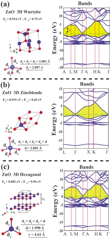
III. 3D BULK AND 2D HONEYCOMB ZnO CRYSTAL We first consider 3D bulk ZnO, which are in wurtzite 共wz-ZnO兲, zincblende 共zb-ZnO兲, and hexagonal 共h-ZnO, or graphitelike兲 crystals. Atoms in wz-ZnO and zb-ZnO
struc-tures are fourfold coordinated through tetrahedrally directed sp3orbitals whereas the atoms in h-ZnO crystal are threefold coordinated through sp2 orbitals. Wurtzite structure is found to be the thermodynamically most stable phase of ZnO. The cohesive energy per Zn-O pair is calculated by using the expression
EC= ET关ZnO兴 − ET关Zn兴 − ET关O兴 共1兲
in terms of the total energy of the optimized crystal structure of ZnO, ET关ZnO兴 per Zn-O pair, the total energies of free Zn
and O atoms ET关Zn兴 and ET关O兴. The equilibrium cohesive
energies of wz-ZnO, zb-ZnO, and h-ZnO structures are found to be 8.934, 8.919, and 8.802 eV per Zn-O pair, re-spectively. For wz-ZnO crystal, the hexagonal lattice con-stants of the optimized structure in equilibrium are a = 3.280 Å and c/a=1.616. The deviation of c/a from the ideal value of 1.633 imposes a slight anisotropy in the lengths of tetrahedrally directed Zn-O bonds. While the length of three short bonds is 2.001 Å, the fourth bond is slightly longer and has the length of 2.007 Å. The zincblende structure in Td symmetry has cubic lattice
con-stant a = 3.266 Å and four tetrahedrally coordinated Zn-O bonds having uniform length, d = 2.001 Å. The h-ZnO struc-ture has hexagonal lattice constants a = 3.448 Å, c/a = 1.336, and d = 1.990. The structural parameters of these three bulk ZnO crystals are shown in Fig.1. The lattice con-stant of wz-ZnO, a共c/a兲 is measured between 3.247 共1.6035兲 Å and 3.250 共1.602兲 Å using different methods.33
The calculations based on ab initio linear combination of atomic orbitals method with all-electron Gaussian-type basis set predict a = 3.286 Å and c/a=1.595.34All our results
re-lated with the structural parameters are in good agreement with the experimental and theoretical values within the aver-age error of ⬃1%.33,34
The optimized atomic structure and corresponding elec-tronic band structure of 3D ZnO crystals are presented in Fig. 1. All wz-ZnO, zb-ZnO, and h-ZnO crystals are direct band-gap semiconductors with calculated band gaps being EG= 0.75, 0.65, and 0.96 eV, respectively. Highest valence
band has O-2p character; the states of the lowest conduction band is formed from Zn-4p and Zn-4s orbitals. Valence band consists of two parts separated by a wide intra-band gap. The lower part at⬃−18 eV is projected mainly to O-2s orbitals. The upper part is due to mainly Zn-3d and O-2s orbitals. The differences in the band structure of different three 3D crys-tals become pronounced in the lower part of the conduction band. It should be noted that the band gaps of bulk ZnO is highly underestimated by DFT calculations.35 The
experi-mentally measured band gap of wz-ZnO is ⬃3.37 eV at room temperature.33We performed GW
0calculations to cor-rect the band gaps calculated within GGA. Our results for wz-ZnO, zb-ZnO, and h-ZnO are, respectively, 3.29, 3.04, and 3.32 eV. As for earlier studies, calculations with GW corrections reported a band gap of 3.59 eV for zb-ZnO.36All
electron linearized augmented planewave 共LAPW兲 calcula-tions predicted the band gap of wz-ZnO 0.77 eV using local-density approximation 共LDA兲, which is corrected by GW calculations to 2.44 eV.37
Charge transfer from Zn atoms to O atoms is a measure of the ionicity of ZnO crystal. We calculated the amount of charge on constituent Zn and O atoms in 3D crystals by performing the Löwdin analysis38 in terms of the projection
of plane waves into atomic orbitals. By subtracting the va-lencies of free Zn and O atoms from the calculated charge
values on the same atoms in 3D crystals we obtain the charge transfer ␦q from Zn to O. The calculated value of charge transfer for wz-ZnO, zb-ZnO, and h-ZnO is found to be 1.41 electrons. The values of charge transfer calculated with the Bader analysis39 are␦q = 1.22, ␦q = 1.17, and ␦q = 1.20
elec-trons for wz-ZnO, zb-ZnO, and h-ZnO, respectively. Same analysis performed with local basis set using SIESTA 共Ref. 31兲 yields significantly lower values of charge transfer, ␦q = 0.90, ␦q = 0.88, and ␦q = 0.91 electrons for wz-ZnO, zb-ZnO, and h-zb-ZnO, respectively. This analysis clearly indicates that a significant amount of charge is transferred from low electronegative Zn atom to high electronegative O atom. However the values of␦q may scatter owing to the ambigu-ities in placing boundary between Zn and O in crystalline structure.
IV. 2D ZnO HONEYCOMB STRUCTURE
The structure of monolayer ZnO is optimized using peri-odically repeating supercell having hexagonal lattice in 2D and the spacing of 10 Å between ZnO planes. The optimized structure was planar and the magnitudes of the Bravais vec-tors of the hexagonal lattice are found to be a1= a2 = 3.283 Å, and the Zn-O bond, d = 1.895 Å 共see Fig. 2兲. In
contrast to 2D puckered honeycomb structures of Si, Ge, and compounds of III and V group elements both lying below the first row, any honeycomb structure including one element from the first row form planar honeycomb structure such as graphene, BN, and SiC.13 2D monolayer of ZnO forming
planar honeycomb structure is not an exception. The calcu-lated structural parameters are significantly larger than those of graphene and BN honeycomb structure due to fact that Zn has larger radius40 than that of B, C, N, and O atoms. The
planar structure of 2D ZnO is tested by displacing Zn and O atoms arbitrarily from their equilibrium positions by 0.5 Å and subsequently by reoptimizing the structure. Upon opti-mization the displaced atoms have recovered their original positions in the same plane. It should be noted that the length of Zn-O bonds of 2D ZnO honeycomb structure is smaller than that in the 3D bulk共wz, zb兲 crystals since sp2bonding in the former is stronger than the tetrahedrally coordinated
ZnO 3D Wurtzite EC= 8.934 eV ; EG= 0.75 eV
(a)
c a b d4 d3 d2 d1 d1= d2= d3= 2.001 A d4= 2.007 A oEnergy
(eV)
Bands
EF Γ Α LΜ ΓΑ Η Κ -20 -15 -10 -5 0 5 10 15 EF ZnO 3D Zincblende EC= 8.919 eV ; EG= 0.65 eV(b)
c a b d4 d3 d2 d1 d1= d2= d3= d4= d d = 2.001 Ao ZnO 3D Hexagonal EC= 8.802 eV ; EG= 0.96 eV(c)
a b cd
3d
2d
1 d1= d2= d3= d d = 1.990 AoBands
Γ X K Γ LEnergy
(eV)
-20 -15 -10 -5 0 5 10 15Energy
(eV)
-20 -15 -10 -5 0 5 10 15Bands
Γ Α LΜ ΓΑ Η Κ c = 4.61 Ao c/2FIG. 1.共Color online兲 Cohesive energies ECper Zn-O pair, band gaps EG, Zn-O bonds, atomic and energy band structures of 3D共a兲
wurtzite,共b兲 zincblende, and 共c兲 hexagonal crystals of bulk ZnO. Red-small and blue-large balls correspond to O and Zn atoms, re-spectively. The gap between valence and conduction bands are shaded and the zero of energy is set at the Fermi level EF. All
structures including lattice constants are fully optimized.
0 100 200 300 400 500 600 700
Γ
M
K
Γ
Zn O a1 a2 2D Wavenumber (cm ) -1FIG. 2. 共Color online兲 Phonon-dispersion curves calculated by force-constant method for 2D monolayer ZnO. Atomic structure and hexagonal lattice vectors are shown by inset.
sp3 bonding in the latter. Similar trend is also found in C, BN, and SiC honeycomb structures. The interaction between ZnO planes appears to slightly weaken the Zn-O bonds of h-ZnO crystal. As a result the length of the Zn-O bonds becomes larger than that of 2D ZnO honeycomb structure. The cohesive energy of 2D monolayer of ZnO is calculated to be 8.419 eV per Zn-O pair. This energy is 0.5 eV smaller than that of 3D wz-ZnO.
A. Atomic structure and stability analysis
It should be noted that 2D honeycomb structure deter-mined by the structure optimization using conjugate gradient method may not be necessarily stable. One needs more strin-gent tests to assure the stability of this truly 2D structure. As a matter of fact, it was argued earlier that any crystal struc-tures consisting of a truly 2D monolayer crystals cannot be stable.41,42 Here, we summarize our analysis on the stability of planar 2D hexagonal structure of ZnO using calculation of phonon-dispersion curves as well as ab initio finite-temperature molecular-dynamics calculations.
We calculated optical and acoustical branches of phonon frequency using the density-functional perturbation theory with plane-wave method as implemented inPWSCFsoftware and the force-constant method43with forces calculated using VASP. The former method includes the polarization effects so that the splitting of longitudinal- and transverse-optical modes at the⌫ point 共namely, LO-TO splitting兲 is obtained. The force-constant method cannot yield the LO-TO splitting and is also very sensitive to the mesh size in calculating forces under atomic displacements and hence in setting up the dynamical matrix. In fact, the imaginary frequencies of ZA branch 共so-called out-of-plane acoustical branch兲 occur around the ⌫ point as an artifact of insufficient mesh size. However, all imaginary frequencies around the⌫ point 共cor-responding to an instability to be induced by acoustical waves with large 兲 are removed by using very fine mesh. Earlier, imaginary frequencies of ZA modes near the⌫ point calculated for 2D honeycomb structures of Ge and III-V compounds inducing similar fortuitous instabilities for large were also removed by using finer mesh.13
In Fig.2we present phonon-dispersion calculated for 2D monolayer of ZnO honeycomb structure using force-constant method, where atomic forces are calculated byVASP. Calcu-lated phonon modes all being positive across the BZ strongly support that 2D monolayer of ZnO is a stable structure cor-responding to a local minimum on the Born-Oppenheimer surface. Our phonon-dispersion curves are in agreement with those calculated in Ref.44.
Furthermore, we have tested the stability of 2D ZnO monolayer using finite temperature ab initio molecular-dynamics 共MD兲 calculations with time steps of 2⫻10−15 s. To lift the constraints to be imposed by a small unit cell, we considered a共7⫻7兲 supercell of the 2D hexagonal ZnO and raised its temperature from 0 to 750 K in 0.1 ps. Then, we have kept the temperature of the system around 750 K for 2.5 ps. While all these calculations resulted in minor defor-mations, the honeycomb structure was not destroyed. It should be noted that these calculations may not be
conclu-sive since 2.5 ps cannot be sufficient to represent all the statistics but this picture is the best one can see from the exiguous window limited by the computational cost imposed by ab initio MD method. In the following sections we will present additional arguments related with electronic ture, which further corroborate the stability of 2D ZnO struc-tures.
B. Electronic structure
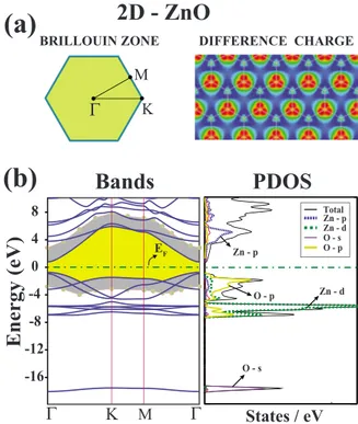
The difference charge density and the electronic energy bands together with the partial density of states共PDOS兲 are presented in Fig. 3. Contour plots of total charge indicate high density around O atoms. The difference charge density is calculated by subtracting charge densities of free Zn and O atoms from the total charge density of 2D ZnO, i.e., ⌬ =ZnO−Zn−O. High-density contour plots around O atoms protruding toward the Zn-O bonds indicate charge transfer from Zn to O atoms. This way the Zn-O bond acquires an ionic character. The charge transfer from Zn to O, ␦q is analyzed by using different schemes. The charge-transfer values calculated by Löwdin method using PWSCF, Bader39 analysis usingVASP, and local basis set analysis usingSIESTA
are, respectively,␦q = 1.35, 1.18, and 0.87 electrons. Interest-ingly, as compared to 3D bulk h-ZnO crystal, the charge transfer from cation to anion of 2D monolayer ZnO is slightly decreased. This is due to the change from sp3hybrid
2D - ZnO
(a)
(b)
Bands
-16 -12 -8 -4 0 4 8Energy
(eV)
PDOS
Κ MΓ
States / eVΓ
DIFFERENCE CHARGE EF Total Zn - p Zn - d O - s O - p O - s Zn - d O - p Zn - p BRILLOUIN ZONEΓ
M KFIG. 3. 共Color online兲 Electronic structure of the 2D monolayer of ZnO.共a兲 Brillouin zone corresponding to 2D hexagonal lattice and difference charge density, ⌬. 共b兲 Energy band structure and density of states projected to the selected orbitals共PDOS兲 of con-stituent atoms. The band gap is shaded共painted in yellow兲 and the zero of energy is set at the Fermi level. Band edges corrected by GW0are indicated by small共light blue兲 circles. The band gap en-larged after GW0correction is shaded共painted light blue兲.
orbital in h-ZnO to sp2 hybrid orbital in honeycomb structure.
Two dimensional ZnO is a direct band-gap semiconductor with a gap value of 1.68 eV. However, the actual band gap is expected to be larger. The bands are corrected using GW0 method32 and the direct band gap at the ⌫ point of BZ is found to be 5.64 eV. Much recently, it has been reported that the band gap of 2D-ZnO is calculated to be 3.57 eV with GW corrections.44 Similar to the bands of 3D bulk ZnO crystals,
the upper part of the upper valance band are derived mainly from O-2p orbitals whereas the lower part has Zn-3d char-acter. The bands at the edges of conduction and valence bands along the⌫-K direction are derived from bonding and antibonding combination of O-2pzand Zn-4pzorbitals
form-ingandⴱstates. The highest valence band along the⌫-K direction has mainly O-2pz but small Zn-4pz orbital
contri-bution while the lowest conduction band is composed mainly from Zn-4pz but small O-2pzorbitals. Small Zn-4pz
contri-bution is also confirmed by PDOS. Consequently, planar ge-ometry of 2D monolayer of ZnO is expected to be attained by the bonding combination of pzstates. The same situation
occurs for 2D monolayer of BN honeycomb structure, which is an ionic III-V compound with wide band gap between and ⴱ states. The planar stability graphene is also main-tained bybonds.
C. Vacancy defects and antisite
It was shown that vacancies have remarkable effects on electronic and magnetic properties of 2D graphene and graphene nanoribbons.45–50 The effects of vacancies in
monolayer of ZnO have not been treated yet. It was reported that the vacancy defects can be intentionally created by electron-irradiation method23 on ZnO thin films. We
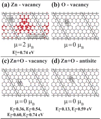
investi-gated the effects of Zn, O, Zn+ O divacancy and O + Zn an-tisite in a periodically repeating 共5⫻5兲 as well as 共7⫻7兲 supercells. The vacancy-vacancy coupling in the larger 共7 ⫻7兲 supercell was reduced significantly. Flat bands in the band gap have charge density localized at the defect site. The width of these flat bands can be taken as the measure of the strength of the direct and indirect共via the hopping through the orbitals in the lattice兲 vacancy-vacancy coupling. The largest width of such a band is already small 共less than 50 meV兲. The average energy of these flat bands from the top of the valence band can be taken as the localized states of an individual vacancy defect. Our results obtained using a 共7 ⫻7兲 supercell are presented in Fig. 4 and discussed in the rest of the section.
The GGA band gap of a defect-free, 2D monolayer ZnO increases by ⬃0.08 eV in a 共7⫻7兲 supercell including a vacancy defect. This is an artifact of the model, which mim-ics an individual vacancy in supercell having limited size. First we generated a Zn vacancy by removing a single Zn atom from the monolayer of ZnO in honeycomb structure as shown in Fig. 4共a兲. Upon the structure optimization, two O atoms around vacancy are departed from the plane. Similar to the vacancies in graphene and BN, Zn vacancy induces a local magnetization in the system. Isovalue surfaces of spin-density difference ⌬ clearly reveals the magnetism around
vacancy. The calculated total magnetic moment is 2B per
unit cell. Note that similar Zn vacancy in the 3D bulk ZnO crystal induces a magnetic moment of ⬃1B. It should be
noted that the magnetic moment of Zn vacancy arises from the unpaired electrons of oxygen atoms around the Zn va-cancy. Therefore it is important to determine precisely whether the vacancy-induced localized states are occupied. The positions of these localized states of 2D ZnO calculated for the共7⫻7兲 supercell and their occupancy unambiguously comply with the calculated magnetic moment. The Zn va-cancy in a repeating共7⫻7兲 supercell also modifies the elec-tronic structure. The value of the band gap of defect-free ZnO changes from 1.68 to 1.75 eV and a spin-up localized state appear 0.25 eV above the top of the valence band. Fig-ure 4共b兲 presents our results for O vacancy. Unlike the case of Zn vacancy, the monolayer of ZnO containing an O va-cancy is nonmagnetic. Zn atoms around vava-cancy with coor-dination number 2 prefer to stay in the same plane of the other atoms and do not induce any magnetization. The band gap is slightly modified to 1.80 eV. As for Zn+ O divacancy in Fig. 4共c兲, it is again nonmagnetic. The band gap is also modified to 1.46 eV. Four occupied states associated with divacancy occur as localized states in the band gap. Finally, we consider the antisite defect. The resulting relaxed
struc-(a)
(b)
(c)
(d)
Zn - vacancy
O - vacancy
Zn+O - vacancy
Zn+O - antisite
∆ρ=ρ( )−ρ( )
µ=2 µ
Βµ=0 µ
Β O Zn Zn O O Zn O Znµ=0 µ
Βµ=0 µ
Β E1= 0.36, E2= 0.54, E3= 0.60, E4= 0.74 eV E1= 0.74 eV E1= 0.13, E2= 0.59 eVFIG. 4. 共Color online兲 Vacancy defects in a 共7⫻7兲 supercell of the monolayer of ZnO.共a兲 Relaxed atomic structure around the Zn vacancy with isosurfaces of the difference charge density of spin-up and spin-down states, ⌬=共↑兲=共↓兲. Energies Ei of localized states measured from the top of the valance band and the net mag-netic moment per supercell in Bohr Magneton B. Blue-large and red-small balls indicate Zn and O atoms indicated by arrows.共b兲 O vacancy.共c兲 Zn+O divacancy. 共d兲 O+Zn antisite where neighbor-ing O and Zn atoms are exchanged. The 共7⫻7兲 supercells each including one type of various vacancy defects are delineated by solid lines.
ture is given in Fig.4共d兲. The antisite O is pushed away from Zn atoms and makes bonds with a nearby O atom. The sys-tem does not show any magnetization. The energy of final structure with antisite defect is⯝5 eV higher 共i.e., energeti-cally less favorable兲 that of the defect-free 2D monolayer of ZnO. The antisite induces two localized states in the band indicated in the figure. Also it is noted that the magnetic moments calculated for single Zn and O vacancy do not agree with Lieb’s theorem,51 which predicts the amount of
magnetic moments for carbon vacancies in 2D graphene. Ac-cording to Lieb’s theorem, the net magnetic moment per cell is expected to be = 1B for Zn and O vacancies in Fig.4.
This might be related with the ionic bonding which is differ-ent from graphene or the existence of d orbitals in Zn. On the other hand, zero magnetization for Zn+ O divacancy in Fig.
4共c兲is in agreement with the theorem. D. 2D ZnO bilayer
Recently, Tusche et al.20revealed two monolayer of ZnO
grown on Ag共111兲 substrate using surface x-ray diffraction and scanning-tunneling microscopy. They also showed that the transition to the bulk wz-ZnO structure occurs in the 3–4 monolayer coverage. The Zn-O bond length of the planar hexagonal structure measured 1.93 Å is slightly larger than the value of 1.895 Å calculated for the bond length of the monolayer of ZnO. This situation implies that the effect of the Ag共111兲 substrate may be negligible.20
We investigated the atomic structure and stability of bi-layer ZnO honeycomb structure. To determine the minimum-energy configuration we used periodic supercell geometry and considered five different stacking types which are T1, T2, H1, H2, and H3. In T1 configuration, Zn 共O兲 atoms of the second layer are on top of the Zn共O兲 atoms of the first layer. T2is similar to T1except that Zn atoms are above O atoms. H1, H2, and H3configurations are obtained by shifting one of the layers of T1 and T2 on the other layer so that Zn or O atoms of the second layer are placed above the center of the hexagons in the first layer. It is H1共H2兲 if O 共Zn兲 atoms of both layers face the centers of hexagons. H3corresponds to the configuration where O 共Zn兲 atom of the first共second兲-layer face the center of second共first兲 layer.
Among these five configurations we found that T2 is en-ergetically most favorable. H3, H2, H1, and T1configurations have respectively 0.213, 0.312, 0.320, and 0.321 eV 共per primitive cell兲 higher energies than T2 configuration. The length of Zn-O bonds as well as the charge transfer from Zn to O in T2 configuration is slightly larger than the value of 1.895 Å calculated for the bond length of the monolayer of ZnO. This trend complies with the above discussion that the bond length increases by going from 2D monolayer to 3D bulk and implies that the effect of the Ag共111兲 substrate may be negligible.20
The bilayer binding energy among two ZnO layers is cal-culated to be 0.162 eV 共per Zn-O pair兲 by subtracting the total energies of two individual monolayers from the total energy of bilayer ZnO in T2 configuration. Furthermore the layer-layer separations are calculated as 4.02, 2.36, 3.80, 3.78, and 2.68 Å for T1, T2, H1, H2, and H3, respectively.
Hence, bilayer formation is exothermic. The calculations with LDA, which accommodate van der Waals interaction between layers better, yields 0.297 eV共per Zn-O pair兲 bind-ing energy between two ZnO layers and 2.267 Å layer-layer separation in T2structure. The layer-layer separation for T2is experimentally reported as 2.314 Å.20 The difference be-tween the lattice constants of the monolayer 2D ZnO honey-comb structure and the ZnO bilayer is small. Owing to the relatively weak coupling between two ZnO monolayers, the calculated electronic structure is similar to that of single-layer ZnO honeycomb structure, except that the band gap decreases to 1.44 eV for T2. This band gap increases to 5.10 eV after the GW0 correction, which is still smaller than the GW0 corrected band gap of 2D monolayer ZnO.
We next address the question whether the structure of 2D bilayer formed by the T2stacking of the ZnO bilayer is stable is examined by the finite temperature ab initio molecular-dynamics and phonon-frequency calculations. Ab initio molecular-dynamics calculations at 750 K are performed with the same parameters as done for the monolayer ZnO in previous section indicate that the bilayer remains stable at 750 K after 3.0 ps.
V. DIMENSIONALITY EFFECTS
A comparison of Zn-O bond length, cohesive energy, GGA bad gap, GW0 corrected band gap calculated for 3D wz-ZnO, zb-ZnO, and h-ZnO, and 2D bilayer and monolayer of ZnO are presented in Table I, where interesting dimen-sionality effects are deduced. These dimendimen-sionality effects are believed to be crucial for better understanding of 2D crystals. Quasi-1D nanoribbons are not included to this dis-cussion because of edge effects of the ribbon.
Three dimensional crystals have larger number of nearest neighbors and also posses larger Madelung energy as com-pared to 2D crystals. wz-ZnO appears to correspond to the global minimum of ZnO II-VI compound. However the en-ergy difference between wz-ZnO and 2D monolayer of ZnO is only ⬃0.5 eV and is smaller than one expects. It appears that sp2-like bonding which is stronger than sp3-like bonding and the bonding between adjacent pz orbitals, which
con-tributes to stability by maintaining the planar geometry gives rise to the relatively smaller energy difference between 3D bulk and 2D monolayers of ZnO. In the absence of signifi-cant bonding one expects that 2D planar ZnO would be buckled共puckered兲 for stability as found in 2D Si and GaAs honeycomb structure.12,13 Through puckered planar sp2 or-bital is dehybridized and is transformed to sp3-like hybrid orbitals. Here we note that population of oxygen sp2 and p
z
orbitals is larger than that of corresponding Zn orbitals since the former significantly higher electronegativity.
Interestingly, while GGA bad gaps of 3D ZnO occurs 0.75–0.96 eV, the band gaps of in 2D is 1.68–1.44 eV. The band gap in 2D is larger than 3D since the energy difference between sp3-like orbitals of Zn and O ions is smaller than the energy difference in sp2 orbitals. The latter gives rise to larger energy difference between bonding and antibonding orbitals. These band gaps are, however, underestimated by GGA since they increase approximately three times upon
GW0 corrections. It appears that band-gap values corrected by GW0is closer to experimental value and hence superior to GW correction. As for as dZn-O, ECand EGare concerned, 3D
h-ZnO is intermediate between 3D and 2D structures. Also calculated values of bilayer ZnO are slightly closer to 3D than those of 2D monolayer of ZnO.
Charge transfer from Zn to O is crucial for dimensionality effects but difficult to calculate precisely. Charge transfer,
␦q, calculated using three different schemes, namely, Löw-din, Bader, and Siesta, yield different but consistent values. For example, the Löwdin values occur around 1.4 electrons for 3D but relatively smaller value of 1.35 electrons for 2D. Bader analysis yields 1.22–1.20 electrons for 3D and rela-tively smaller value of 1.18 electrons for 2D. As for Siesta, 3D values, they are 0.90 electrons for 3D but 0.87 electrons for 2D. Excluding the paradoxical situation with charge-transfer values of zb-ZnO occurring close to those of 2D ZnO, the charge transfer between Zn and O is slightly smaller in 2D than 3D.
VI. ZnO NANORIBBONS
In this section, we consider bare and hydrogen-passivated armchair 共a-ZnO兲 and zigzag 共z-ZnO兲 ZnO nanoribbons. These nanoribbons are specified according to their width given in terms of n number of Zn-O pairs in their unit cells. Hence, z-ZnO共n兲 indicates a zigzag ZnO nanoribbons having n Zn-O pairs in their unit cell. We investigate their elec-tronic, magnetic, and mechanical properties. First, we start with the stability analysis of these nanoribbons.
A. Stability analysis
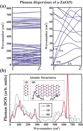
We have analyzed the stability of the bare armchair ZnO nanoribbons having n = 9 Zn-O atom pairs in the unit cell using the force-constant method and the finite-temperature molecular-dynamics calculations. The dynamical matrix was generated using the forces calculated in seven unit cells of a-ZnO共9兲. Results of this calculation were presented in Fig.
5共a兲. Phonon-dispersion curves of quasi-1D nanoribbons, in general, show profiles expected from the folding of 2D phonon-dispersion curves. Modes appearing above
700 cm−1, however, are not expected from this folding. They were attributed to edge effects and reconstructions.
Right panel of Fig.5共a兲presents the acoustic region in ten times magnified scale. There are four acoustic modes, disper-sion curves of which go to zero as k→0. To get exactly zero value, we have imposed the symmetries originating from translational and rotational invariance on the dynamical ma-trix. To impose these symmetries we have tuned the force-constant matrix elements so that all forces on all atoms are zero when the whole structure is shifted in three dimensions or slightly rotated along the axis passing through the middle of the nanoribbon.
Both the longitudinal and transverse-acoustic modes have linear dispersions near the ⌫ point. Group velocity of LA mode is slightly higher than that of TA mode. Out of plane ZA and twisting acoustical TW modes52 have quadratic
dis-persion near the ⌫ point, which is attributed to the rapid decay of the force constants with increasing neighbor dis-tance. In fact there are some imaginary frequencies in ZA mode near the⌫ point. The absolute value of these frequen-cies do not exceed 0.5 cm−1 and they are purely an artifact of the precision of the numerical calculation. Using a finer mesh makes these imaginary frequencies disappear.
We also have calculated vibrational modes of the finite patch of ZnO having the length of five unit cells and the width of n = 9. Zigzag edges of this flake were saturated by hydrogen atoms to eliminate the magnetism and to simplify the numerical computations. Vibrational spectrum of this structure had no imaginary frequencies implying the fact that finite-size flakes of 2D ZnO honeycomb structure is stable. The DOS of calculated phonon frequencies are presented in Fig.5共b兲. Note that, DOS calculated for three different hon-eycomb systems are similar. Owing to the edge effects the gap between the acoustical and optical branches of the rib-bon is reduced. Similar effect as well as broadening of discrete-mode frequencies cause DOS of the flake to deviate significantly from that of 2D honeycomb structure in the gap. The vibrational modes attributed to strong Zn-H and O-H bonds are centered, respectively, at 1830 and 3700 cm−1. These modes are not shown since these frequencies are be-yond the range of Fig.5共b兲.
Ab initio molecular dynamic calculations were also car-TABLE I. A comparison of bonding共or type of hybrid orbitals兲, the length of Zn-O bond dZn-O, cohesive
energy per Zn-O pair EC, band gap EGcalculated with GGA and corrected by G0W0and GW0in the present study, earlier GW calculations, and experimental value.
ZnO Bonding dZn-O
EC
共eV/atom兲 GGA G0W0 GW0 GW Experiment
3D wz sp3 2.001–2.007 8.934 0.75 2.76 3.29 2.44a 3.37d 3D zb sp3 2.001 8.919 0.65 2.53 3.09 3.59b 3D h sp2+ p z+ VdW 1.999 8.802 0.96 2.84 3.32 2D bilayer sp2+ pz+ VdW 1.932 8.640 1.44 4.45 5.10 2D monolayer sp2+ p z 1.895 8.478 1.68 4.87 5.64 3.57c aReference37. bReference36. cReference44. dReference33.
ried out for a-ZnO共9兲 and a finite-size patch of it. To elimi-nate constraints to be imposed by small unit cell, the infinite nanoribbon is treated by a supercell composed of five unit cells. Both nanoribbons are kept at 750 K for 3.5 ps. As a result, infinite, periodic structure of a-ZnO共9兲 composed of five unit cells had minor reconstructions at the edges while its honeycomb structure was preserved. Finite structure had the similar pattern at the armchair edges but the reconstruc-tions at the hydrogen-saturated zigzag edges were more pro-nounced. These reconstructions made the whole system bend but again the honeycomb structure was preserved around the central region of the nanoribbon. The results of this analysis are interpreted that finite-size ZnO nanoribbons are stable.
B. Electronic and magnetic properties
Bare and hydrogen-terminated a-ZnO nanoribbons are nonmagnetic semiconductors with direct band gaps which are relatively larger than that of the monolayer ZnO. Figures
6共a兲 and 6共b兲 show the atomic and electronic structure of bare and hydrogen-terminated a-ZnO共n兲 with n=9. The at-oms at the edges of the bare a-ZnO are reconstructed; while one edge atom, Zn is lowering, adjacent edge atom, O is raised. The energy band gap calculated with GGA is direct and 1.92 eV wide and is larger than the band gap of 2D monolayer ZnO. Band-decomposed charge-density analysis of a-ZnO共9兲 is presented in Fig.6. The highest valance bands are degenerate and their charge accumulates on oxygen edge atoms for bare ribbon. The third band from the top of valence band is also associated with edge states. On the other hand, the charge of the lowest conduction band is distributed uni-formly in the ribbon. The charge of the second conduction band is mostly distributed at the dangling bonds on the edges of the ribbon.
The passivation of Zn and O atoms at the edges by hy-drogen atoms gives rise to changes in the electronic band 0 100 200 300 400 500 600 700 800 Wavenumber (cm )-1
Phonon
DOS
(arb.
units)
2D 1D 0DΓ
Z
1D 0D Atomic Structures H Wavenumber (cm ) -1(a)
(b)
Zn O 0 10 20 30 40 50 60 70 80 0 100 200 300 400 500 600 700 800Γ
Z
Wavenumber (cm ) -1Phonon dispersions of a-ZnO(9)
LA TA
TW ZA
FIG. 5.共Color online兲 共a兲 Phonon-dispersion curves of a-ZnO共9兲 calculated by force-constant method. Right panel presents the mag-nified view of the low-lying modes. Here the well-known out-of-plane, transverse, and longitudinal acoustical modes are labeled, respectively, as ZA, TA, and LA. The fourth acoustical twisting mode, which is indigenous to quasi-1D nanoribbons, is labeled as TW, because this mode corresponds to the twisting of the nanorib-bon along the axis passing through the middle of the ribnanorib-bon in the infinite direction.共b兲DOS calculated for 2D planar ZnO 共shown by solid lines兲; armchair a-ZnO共9兲 共shown by dashed lines兲; and a finite-size flake, i.e., a 5 unit cell long a-ZnO共9兲 共shown by dotted lines兲. The discrete frequencies due to finite-size structure are Gaussian broaden with =8 cm−1in order to compare with con-tinuous DOS of 2D layer and quasi-1D ribbon. Quasi-1D 共nanorib-bon兲 and 0D 共flake兲 honeycomb structures are shown by inset.
FIG. 6. 共Color online兲 Atomic and electronic structure of bare and hydrogen-terminated armchair nanoribbons a-ZnO共9兲. 共a兲 Atomic structure with unit cell comprising n = 9 Zn-O atom pairs, energy band structure and charge-density isosurfaces of selected states of bare nanoribbons. The charge of the bands of edge states are localized at the edge atoms.共b兲 Same as 共a兲 but for hydrogen-passivated nanoribbon. Large, medium, and small balls indicate Zn, O, and H atoms, respectively. Unit cells are delineated by dashed lines.
structure. The bond lengths Zn-H and O-H bonds are calcu-lated to be 1.53 and 0.97 Å. As seen in Fig. 6共b兲, upon passivation with hydrogen atoms, the reconstruction of edge atoms are weakened. At the end the edge state bands are discarded from the band gap and replaced by dispersive bands having charge distributed uniformly in the ribbon. The band gap of H-passivated a-ZnO共9兲 slightly increases to ⬃1.98 eV.
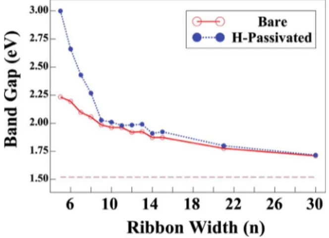
The variation in the band gap EGfor the bare and
hydro-gen saturated armchair nanoribbons as a function of n is given in Fig. 7. The band gaps are large for small n but approaches to those of 2D honeycomb structure as the width n→⬁. This is an indication of the quantum-size effect. For n⬍9, the value of the band gap of hydrogen-passivated a-ZnO is significantly larger than that of bare ribbons; the difference practically disappears for n⬎20. In contrast to graphene and BN nanoribbons, family-dependent variations in band gap53 is absent in Fig. 7. The variation in the band
gap with n is an important property, which may lead to for-mation of quantum dot or multiple quantum wells through the size modulation.8
Earlier it has been reported54,55 that all a-ZnO nanorib-bons are semiconductors with a constant band gap of 2 eV. In our case, however, the band gaps of nanoribbons, especially for n⬍10, display apparent dependency on n. The tendency of the decrease in the band gaps to the 2D ZnO band gap is also observed when n is increased.
In contrast to a-ZnO nanoribbons, all zigzag nanoribbons 共z-ZnO兲 we investigated in this work 共namely, n=5,7,9兲 show metallic character regardless of their widths. On the other hand, while all a-ZnO nanoribbons are nonmagnetic, bare z-ZnO nanoribbons are magnetic due to edge states. The magnetic properties of z-ZnO depend on whether the edge atoms are passivated with hydrogen. Our results regarding with the bare and hydrogen-passivated z-ZnO共n兲 nanorib-bons for n = 9 are presented in Figs. 8共a兲–8共c兲. In Fig. 8共a兲, while the upper edge of the ribbon is made by O atoms, the lower edge terminates with Zn atoms. The bare z-ZnO nan-oribbon is magnetic since the spin-polarized calculations yield the total energy, which is energetically 34 meV favor-able than that obtained from spin-unpolarized calculations.
The total magnetic moment of the system was calculated as 0.57Bper unit cell. Figure 8共b兲shows total DOS and band
structure of bare z-ZnO共9兲 together with isosurface charge densities of selected bands. Bare z-ZnO共9兲 have isosurfaces of difference charge density⌬ occur around O edge atoms due to unpaired O-2p orbitals. Clearly, bare z-ZnO is a fer-romagnetic metal. These results are in agreement with those predicting that the ferromagnetic behavior of ZnO nanorib-bons due to unpaired spins at the edges is dominated by oxygen atoms.54,55
The band structure of the nanoribbon gives us further in-formation about the magnetism of the system. When we plot the spin-up and spin-down bands we observe the splitting of these bands around Fermi level. The conduction and lower valance bands are degenerate for spin-up and spin-down states, some of which are shown with yellow isosurface charge densities in the figure. We also plotted charge density of two states of spin-split nondegenerate bands. Spin-down state is half filled while spin-up state is totally filled. Further-more, their charges are confined to the O edge of the ribbon. The spin polarization at the Fermi level is calculated in terms of density of spin-up and spin-down states, D共↑, ↓ ,EF兲,
namely, P共EF兲=兩D共↑,EF兲−D共↓,EF兲兩/关D共↑,EF兲+D共↓,EF兲兴
and is around 80% for spin-down states although the spin-up states are majority spins. This suggests z-ZnO共n兲 with high spin polarization at EF can operate as spin-valve device.
As we discussed in Sec. IV C, the magnetism of Zn va-cancy in the monolayer ZnO is directly related with O atoms having unpaired 2p orbitals. Similarly, bare z-ZnO nanorib-bons have also magnetic states on O terminated edge of the ribbon. The splitting of spin-up and spin-down bands around Fermi level is removed when the edges of bare z-ZnO共9兲 in Fig.8共a兲is passivated by hydrogen. The resulting structure is again metallic but nonmagnetic. The electronic properties of the z-ZnO共9兲 ribbon passivated with hydrogen is presented in Fig.8共c兲. Two bands just below the Fermi level are local-ized on the Zn edge of the ribbon and lowest conduction band is localized on the O edge of the ribbon. Similar results are also obtained for n = 5 and n = 7. The situation regarding the magnetism of bare z-ZnO is somewhat different from that of the bare zigzag graphene nanoribbons, which have ferromagnetic coupling along the edges but antiferromag-netic coupling between the edges.5Moreover, unlike the case
in z-ZnO nanoribbons, the magnetism of zigzag graphene nanoribbons are not destroyed upon termination of edges with hydrogen atom.
An important feature of zigzag ZnO nanoribbons is that charged Zn and O atoms terminate different edges and thus induce sizable electric-dipole moments. For the bare z-ZnO共9兲 the dipole moment is calculated to be 0.78共electron⫻Å兲 per cell. Upon H termination of Zn and O edge atoms the dipole moment increases to 1.07共electron ⫻Å兲 per cell and its direction is reversed. While the dipole effects are included in the electronic-structure calculations of H-terminated z-ZnO共9兲 nanoribbons, the band gap underes-timated by GGA may effect its metallicity. Unfortunately, GW0 corrections cannot be applied due to large number of atoms.
FIG. 7. 共Color online兲 Variation in the calculated band gaps of bare and hydrogen-passivated ZnO armchair nanoribbons with their widths n. Dashed line indicates the band gap of the infinite 2D ZnO.
C. Mechanical properties of ZnO nanoribbons The response of the nanoribbons to the applied uniaxial stress is crucial and provides information on the strength of the nanoribbons. More recently, the response of graphene to strain 共or to tension兲 in the elastic deformation range has been an active field of study. For example, recent works56
indicated the effect of deformation on the electronic proper-ties for band-gap engineering. Moreover theoretical studies57
have shown that carbon atomic chain can be derived from graphene under tension. Jin et al.58 showed that carbon
atomic chains can be derived from graphene by electron ir-radiation inside a transmission electron microscope. There-fore, the response of ZnO nanoribbons to tension is of crucial importance.
Owing to ambiguities in defining the cross section of the ribbon one cannot determine the Young’s modulus rigor-ously. We examined the variation in the strain energy, Es共⑀兲
= ET共⑀兲−ET共⑀= 0兲 with respect to the applied uniaxial strain, ⑀=⌬c/c, c being the lattice constant along the ribbon axis. The variation in Es共⑀兲 includes information regarding the
mechanical properties of the ribbon. For example, force con-stant,=2E
T/c2 is obtained from the variation in Es.is
an observable and can specify the strengths of ribbons un-ambiguously. The effects of two edges due to incomplete hexagons becomes important for narrow nanoribbons but de-crease with increasing width. In-plane stiffness C, which is independent of the thickness, can also be used instead of
Young’s modulus. Defining A0as the equilibrium area of the system, C can be given as
C = 1 A0
冉
2E
s
⑀2
冊
. 共2兲By choosing a reasonable thickness “h,“ Young’s modulus can be recalled as Y = C/h. The thickness value around 3.34 Å was used in order to evaluate the elastic properties of SWNTs and graphene by some works in literature.59–61 We note that while C is unique for 2D infinite共periodic兲 honey-comb structure of ZnO, for nanoribbons it depends on how the width of the ribbon is taken in determining A0. In fact, the width of the a-ZnO nanoribbon cannot be determined straightforwardly. It is not clear whether the distance is from Zn at one edge to Zn at the other edge or from O at one edge to other O. One can also take the average of these two or consider charge spill over from these edge atoms. Hence the value of C is subject to small changes depending on how the width of the nanoribbon is taken. This uncertainty, however, diminish as the width increases; eventually the value of C converges to a fixed value. In this respect, once the width is fixed C, can be determined from .
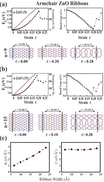
We considered three nanoribbons, a-ZnO共9兲, a-ZnO共15兲, and z-ZnO共9兲. In order to eliminate the constraints imposed by the periodic boundary conditions of small unit cell, cal-culations are performed using a supercell composed of four FIG. 8. 共Color online兲 Bare zigzag nanoribbon z-ZnO共n兲 with n=9: 共a兲 honeycomb structure with primitive unit cell delineated and difference charge density ⌬ of spin-up and spin-down states. 共b兲 Total density of spin-up and spin-down states 共DOS兲, energy band structure, and isosurface charge density of selected spin states. Large, medium, and small filled balls indicate Zn, O, and H atoms, respectively. 共c兲 and 共d兲 are same as 共a兲 and 共b兲. Yellow-light and blue-dark densities are for spin-up and spin-down states. Similarly red-continuous and blue-dashed curves are spin-up and spin-down spin bands. Black lines are for nonmagnetic共spin-paired兲 bands.
primitive unit cells for a-ZnO and five unit cells for z-ZnO. The size of supercells is determined based on certain tests. Figures9共a兲and9共b兲show the variation in the strain energy Es共⑀兲 and band gap EG共⑀兲 with the applied strain, ⑀for both
ribbons, a-ZnO共9兲 and a-ZnO共15兲. They display a parabolic Esvs⑀curves up to the strains⑀⬃0.13. Beyond these strain
values, energy vs strain variation becomes elastic but anhar-monic. In the elastic range, the ribbons preserve their honey-comblike structure but the hexagons are elongated uniformly along the direction of the strain. Zones of harmonic and an-harmonic variation in Es共⑀兲 can be better deduced by
calcu-lating the tension force, FT共⑀兲=−Es共⑀兲/c. FT共⑀兲 is linear
for 0ⱕ⑀ⱕ ⬃0.13 in the elastic-harmonic range but becomes nonlinear for⬃0.13ⱕ⑀as seen in Figs.9共a兲and9共b兲. If the applied tension is released, the elastic deformation in both harmonic and anharmonic ranges disappears and the ribbon returns to its original equilibrium geometry.
The elastic deformation range of a-ZnO共9兲 and a-ZnO共15兲 ends with a sharp fall of the total energy. This point is iden-tified as the yielding point of the ribbon occurring at ⑀ ⯝0.20. The yielding points are followed with structural transformation, where honeycomb cage structure starts to un-dergo a change and part of the strain energy is relieved. Once the yielding point is passed the ribbon can stretch under sig-nificantly low tension and some fraction of the deformation will be permanent and irreversible if the tension is released. Similar behavior occurs when a nanowire of metals, such as Au or Cu; following an order-disorder transformation the elastic deformation ends and the wire is elongated by one lattice constant共or it deforms plastically兲. However, in con-trast to the present case, the nanowire attains again the or-dered state and start to deform elastically.62
The force constant is calculated to be = 2.05 and 3.88 eV/Å2 for a-ZnO共9兲 and a-ZnO共15兲, respectively. The increase infrom 2.05 to 3.88 eV/Å2is due to the increase in the width from n = 9 共⬃12.81 Å兲 to n=15共⬃22.65 Å兲. Note that if the Hooke’s law were valid for these nanorib-bons, the ratio 共15兲/共9兲 would be equal to the ratio of widths, namely, 22.65/12.81= ⬃1.77. The calculated value 共3.88/2.05=1.89兲 is slightly higher. The discrepancy arises from the edges of the ribbons, which respond to tension dif-ferently from the central region. Therefore, deviation from the Hooke’s law becomes more serious as n decreases but diminish as n→⬁.values of a-ZnO共9兲 and a-ZnO共15兲 cal-culated for primitive unit cell are 7.92 eV/Å2共instead of 4 ⫻2.05=8.20 due to numerical calculations performed in a large supercell兲 and 15.04 eV/Å2 共instead of 4⫻3.88 = 15.52兲, respectively. These values are smaller than those corresponding to graphene 共40.96 and 72.52 eV/Å2兲 and BN共34.02 and 60.46 eV/Å2兲 nanoribbons.
The calculated in-plane stiffness values C for a-ZnO共9兲 and a-ZnO共15兲 are 3.75 and 3.71 eV/Å2, respectively.63The
calculated C values of armchair graphene共BN兲 nanoribbons for n = 9 and n = 15 are 18.45 共14.55兲 and 18.85 共14.66兲 eV/Å2, respectively. Graphene and BN nanoribbons have significantly higher in-plane stiffness as compared to a-ZnO nanoribbons. The difference mainly originates from the fact that a-ZnO honeycomb structure has larger unit cell than that of graphene and BN honeycomb structures. In view of the calculated and C values, both graphene and BN nanoribbons are stiffer than ZnO nanoribbons.
Figure 9illustrates also the atomic structure of a-ZnO共9兲
and a-ZnO共15兲 nanoribbons for three different values of ap-plied strain. After the yielding point, the honeycomb struc-ture is destroyed and the polygons being smaller and larger than hexagons form. In some cases, a net magnetic moment can develop in those polygons. The onset of plastic range and variation in atomic structures can depend on the periodic boundary conditions. These artifacts of periodic boundary conditions are eliminated to some extent by using larger su-percells comprising several unit cells. Nonetheless, the plas-tic deformations shown in Figs.9共a兲and9共b兲have still large
0 0.05 0.10 0.15 0.20 0.25 2.59 7.59 12.59 17.59 22.59 1 1.5 2
Armchair ZnO Ribbons
c = 22.88 A o c = 26.99 A c = 29.28 A o o
(a)
=0.00 =0.18 =0.28n=1
5
0 0.05 0.10 0.15 0.20 0.25 Band Gap (eV) Strain Strain a-ZnO (9) c = 22.90 Ao c = 27.48 Ao c = 29.31 Aon=9
=0.00 =0.20 =0.28(b)
1.4 1.8 1.0 Band Gap (eV) 0.6 Tension (eV/A) 0 200 100 o Tension (eV/A) 0 200 100 o 300(c)
a-ZnO (15) Strain 0 0.05 0.10 0.15 0.20 0.25 0 0.05 0.10 0.15 0.20 0.25 Strain E (eV) s 3.64 13.64 23.64 33.64 E (eV) s 5 10 15 20 25 0 1 2 3 4 5 10 15 20 25 0 1 2 3 4 C (eV/A 2) Κ (eV/A 2) 0Ribbon Width (A)
0
0
FIG. 9. 共Color online兲 共a兲 Variation in the strain energy Esand
band gap EGof the bare a-ZnO共n兲 共n=9兲 with the applied uniaxial strain, ⑀ are shown by a curve with squares. Calculated tension shown by tin共red兲 curve is initially linear but deviates from linear-ity for large⑀. Atomic structure for three different values of strain. The boundaries of the supercells comprising four unit cells and corresponding lattice constants c are indicated by vertical lines.共b兲 Same as 共a兲 but for bare a-ZnO共n兲 共n=15兲. 共c兲 Variation in force constant, and in-plane stiffness, C of a-ZnO with the width w of the nanoribbons.
repeat periodicity. Even if the size and forms of polygons appear to be hysteric, their further investigation is of funda-mental interest. The order-disorder structural transformation as well as dislocation generation appear to be absent in this study. The latter may require a treatment of deformation by taking into account very large n and c. Moreover, as pre-dicted for graphene nanoribbons, one expects that the onset of yielding in the presence of vacancy defects and also at high temperature can occur at small strain.57 Nevertheless,
the plastic deformation in the present work is carried out under ideal conditions hence its stochastic nature is not taken into account. The energy gap of the nanoribbon undergoes a significant change under uniaxial tension. It decreases as ⑀ increases and becomes very small at the yielding point. Be-yond the yielding point the band gap increases again.
In Fig. 9共c兲 we plot the calculated values of force con-stant, relative to the width w of a-ZnO共n兲 taken as the distance between outermost atoms of both edges. As ex-pectedis proportional to w and共w兲 can be considered as linear except small deviations from linearity due to edge ef-fects. In fact, 共w兲/w increases slightly with w. Whether a-ZnO共n兲 has even or odd n also causes to a small deviation from single linear variation. As expected, the variation in the in-plane stiffness C with w is not significant. However, C changes significantly between two subsequent values of n.
The zigzag z-ZnO共9兲 nanoribbon displays a variation Es共⑀兲 similar to those of a-ZnO. The calculated value ofis
4.27 eV/Å2, which is larger than that calculated for a-ZnO共9兲 having relatively smaller width. Similarly, in-plane stiffness value of z-ZnO共9兲 is slightly smaller than that of a-ZnO共9兲 and a-ZnO共15兲. C is calculated as 3.24 eV/Å2. The zigzag ZnO共9兲 remains to be ferromagnetic metal in the elastic deformation range but their magnetic moment de-creases with increasing ⑀. However, beyond the yielding point it shows a sharp fall and diminish with increasing⑀in the plastic range as seen in Fig. 10. In contrast to a-ZnO, long polygons are aligned along the axis of the z-ZnO共9兲 in Fig.10.
VII. DISCUSSION AND CONCLUSIONS
This work presents an extensive study on 2D monolayer and bilayer ZnO, and ZnO nanoribbons together with their stability analysis. The monolayer of ZnO is an ionic and nonmagnetic, wide band-gap semiconductor with significant charge transfer from zinc atoms to nearest oxygen atoms. Since DFT normally underestimates the calculated band gaps, the calculated band gap of specific structures are cor-rected by GW0self-energy calculations. ZnO has 2D hexago-nal lattice forming a planar honeycomb structure. Our pre-dictions, which contribute to a better understanding of this material, are emphasized by way of conclusions:共i兲 we have shown that, 2D ZnO monolayer and bilayer, quasi-1D bare nanoribbons of ZnO and 0D patch of ZnO correspond to local minima on the Born-Openheimer surface and thus are predicted to be stable.共ii兲 Ab initio molecular-dynamics cal-culations performed at high temperature corroborate our analysis obtained from the calculation of phonon frequen-cies. 共iii兲 We performed calculations of phonon modes and density of states of phonon frequencies of 2D monolayer, quasi-1D armchair nanoribbon and a finite flake using force-constant method. In particular, we revealed the acoustical twisting mode of armchair nanoribbon.共iv兲 Our study of Zn, O, Zn-O vacancies, and O-Zn antisite indicates that local magnetic moments can be generated only by Zn vacancies. 共v兲 We provided an extensive analysis of the electronic struc-ture of hydrogen terminated as well as bare armchair and zigzag nanoribbons. Armchair ZnO nanoribbons are found to be nonmagnetic semiconductors. The band gaps vary with their widths. The narrow nanoribbons have relatively larger band gap due to the quantum-confinement effect. Bare zig-zag ZnO nanoribbons are ferromagnetic metals. The atoms near the oxygen-terminated edge of the ribbons acquire mag-netic moments. The spin polarization at the Fermi level may attain high values for specific zigzag nanoribbons. However, once O- and Zn-terminated edges are passivated with hydro-gen atoms, the zigzag nanoribbon becomes nonmagnetic metal. These electronic and magnetic properties might be useful for spintronic applications. 共vi兲 We found the minimum-energy stacking of the ZnO bilayer and provided energetics and energy band structure corresponding to this stacking. Accordingly, bilayer ZnO is also a nonmagnetic, wide band-gap semiconductor with slightly smaller band gap as compared to that of monolayer. 共vii兲 We provided an analysis of mechanical properties. ZnO nanoribbons under uniaxial strain show harmonic and anharmonic elastic defor-mation ranges and a yielding point. After yielding, the strain energy exhibits a sharp fall and the nanoribbon deform plas-tically. In the elastic range, hexagons are uniformly deformed but honeycomblike atomic structure is maintained. After yielding point some of the hexagons are modified and recon-struct to different polygons which may be smaller or larger than hexagons. Variation in electronic and magnetic proper-ties with deformation and formation of polygons in the plastic-deformation range are of fundamental interest. Calcu-lation of force constants and in-plane stiffness indicate that the stiffness of ZnO nanoribbons is smaller than those of graphene and BN honeycomb structures.
c = 16.57 Ao c = 19.05 Ao c = 19.88 Ao
ε=0.00 ε=0.15 ε=0.20
n=9
Zigzag ZnO Ribbon
0 0.05 0.10 0.15 0.20 1 1.5 2 2.5 Strain 0.0 0.05 0.10 0.15 0.20 Strain µ( µΒ ) z-ZnO (9) Tension (eV/A) 0 200 100 o 1.87 6.87 11.87 16.87 E (eV ) s
FIG. 10. 共Color online兲 Variation in the strain energy Es,
ten-sion, and magnetic moment per supercell of the bare z-ZnO共n兲 共n=9兲 with the applied uniaxial strain. Atomic structures of the bare z-ZnO共9兲 for three different uniaxial strains. The supercells consist of five unit cells.