phys. stat. sol. (c) 2, No. 7, 2631 – 2634 (2005) / DOI 10.1002/pssc.200461544
© 2005 WILEY-VCH Verlag GmbH & Co. KGaA, Weinheim
AlGaN/GaN HEMT-based fully monolithic X-band low noise
amplifier
R. Schwindt1 , V. Kumar1 , O. Aktas2 , J.-W. Lee3 , and I. Adesida*1 1Micro and Nanotechnology Laboratory and Department of Electrical and Computer Engineering, University of Illinois at Urbana-Champaign, 208 N. Wright Street, Urbana, IL 61801, USA
2
Department of Electrical and Electronics Engineering, Bilkent University, 06800 Bilkent, Ankara, Turkey
3
School of Electronics and Information, Kyung Hee University, Suwon, 449-701, Korea
Received 13 July 2004, accepted 24 September 2004 Published online 8 February 2005
PACS 84.40.Dc, 84.40.Lj, 85.30.De, 85.30.Tv, 85.40.Qx
A fully monolithic AlGaN/GaN HEMT-based low noise amplifier is reported. The circuit demonstrated a noise figure of 3.5 dB, gain of 7.5 dB, input return loss of -7.5 dB, and output return loss of -15 dB at 8.5 GHz. The dc characteristics of individual 0.25-µm × 150-µm transistors were: maximum current density of 1.0 A/mm, maximum transconductance of 170 mS/mm and a threshold voltage of -6.8 V. The devices have a typical short circuit current gain cutoff frequency of 24.5 GHz and a maximum oscillating fre-quency of 48 GHz. The devices demonstrated a minimum noise figure of 1.6 dB with an associated gain of 10.6 dB at 10 GHz.
© 2005 WILEY-VCH Verlag GmbH & Co. KGaA, Weinheim
1 Introduction Transmit/receive (Tx/Rx) modules for microwave radar and communication systems require both a power amplifier for the transmit function and a low noise amplifier (LNA) for the receive function. The performance, reliability, and manufacturability of next-generation military and commercial systems will be advanced through the integration of functionality on a single chip. Gallium nitride-based high electron mobility transistors (HEMTs) are excellent candidates for high power and low noise mi-crowave signal amplification. This is due to the advantageous material properties of the group III-nitrides, such as wide bandgap (3.4 eV for GaN to 6.2 eV for AlN) leading to high breakdown fields (1-3 × 10⁶ V/cm) and high saturated electron drift velocity (2.2 × 107 cm/s). Also, the AlGaN/GaN het-erostructure with its high conduction band offset and high spontaneous and piezoelectric polarizations exhibits high sheet carrier densities in the 1013
cm–2
range. As a result, very high microwave power formance has been demonstrated by AlGaN/GaN-based HEMTs [1–6]. Excellent microwave noise formance has also been demonstrated [7–9]. Because most research has focused on the high power per-formance of these devices, the only AlGaN/GaN HEMT-based low noise amplifier (LNA) reported until very recently was a hybrid circuit [10]. Very recently a few monolithic LNAs have been reported which operated below X-band or which employed sub-quarter micron gate-length devices or both [11–13]. This work reports a fully monolithic AlGaN/GaN HEMT-based LNA operating at X-band and employing a reliable 0.25-µm gate-length technology. The results demonstrate the potential for the integration of a robust low noise amplifier with an ultra-high performance power amplifier in a single technology for next-generation military and communication systems.
2 Device and fabrication The layer used in the present study was grown on a semi-insulating 4H-SiC substrate by MOCVD. The epilayer consists of a buffer, 2-µm undoped GaN, a 3-nm undoped
*
2632 R. Schwindt et al.: AlGaN/GaN HEMT-based fully monolithic X-band low noise amplifier
© 2005 WILEY-VCH Verlag GmbH & Co. KGaA, Weinheim
Al0.25Ga0.75N spacer, a 10-nm Si-doped (~1 × 10 19
cm–3
) Al0.25Ga0.75N charge supply layer, and a 10-nm undoped Al0.25Ga0.75N barrier layer. The average sheet resistance of the sample was 453 Ω/square. The first step for device fabrication was mesa-isolation using Cl2/Ar plasma in an inductively-coupled-plasma reactive ion etch (ICP-RIE) system. Ohmic contacts were formed by rapid thermal annealing of evapo-rated Ti/Al/Mo/Au at 850 °C for 30 s [14]. The 0.25-µm gate-length T-shaped gates (Ni/Au) were de-fined using electron-beam lithography. The transistors had a gate-width of 150 µm and a source-drain spacing of 2.5 µm and were passivated with 200 nm thick silicon nitride.
The integrated circuit fabrication process consisted of the following steps: mesa isolation, ohmic metal, Schottky gates via e-beam lithography, overlay metal, silicon nitride deposition and etch; nichrome resistor; a 1-µm-thick evaporated gold level; and airbridge. In addition to active devices, this process incorporates steps necessary for the realization of passive elements, including low-loss transmis-sion lines, metal-insulator-metal capacitors, spiral inductors, and thin-film resistors which are required for a complete monolithic microwave integrated circuit (MMIC) process. Because the LNA has relaxed requirements with respect to thermal impedance and source ground inductance compared to a high power amplifier, this initial LNA MMIC was designed using coplanar waveguide (CPW)-style transmission lines and passive elements so that backside processing was not required.
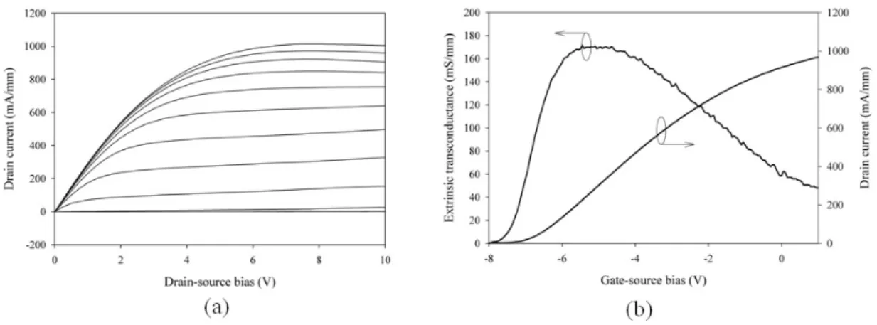
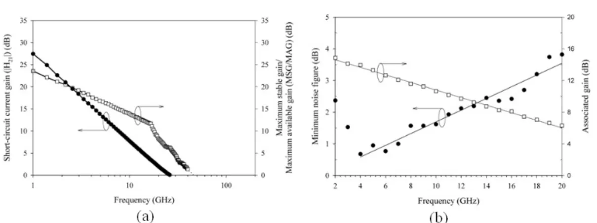
3 Device characteristics Figure 1 shows the DC performance characteristics of a typical 0.25 µm × 150 µm AlGaN/GaN HEMT. It has a maximum drain current density of 1.0 A/mm and a peak DC ex-trinsic transconductance of 170 mS/mm. The threshold voltage is –6.8 V, where the threshold voltage was determined by extrapolating the drain current to zero from the maximum transconductance point. The small signal and noise performance of a typical .25 µm × 150 µm AlGaN/GaN HEMT are shown in Fig. 2. Small signal characteristics were measured using an Agilent 8510B network analyzer. Figure 2(a) shows the short-circuit current gain (|H21|) and the maximum stable gain/maximum available gain
(MSG/MAG) at the device’s peak-fT bias point of 13 V drain-source voltage, –6.0 V gate-source voltage
and 34.6 mA drain current. The fT of the device is 24.5 GHz. The maximum frequency of oscillation fmax
is 48 GHz and is determined by extrapolating the maximum available gain (MAG) at – 20 dB/decade. A Maury/ATN NP5 noise parameter measurement system along with an Agilent 8970B noise figure meter and 8971C noise figure test set was used to measure device noise parameters from 2 to 20 GHz. Figure 2(b) shows the device’s minimum noise figure and associated gain at the device’s minimum noise figure bias of 10 V drain-source voltage, –6.7 V gate-source voltage and 10 mA drain current. The minimum noise figure at 10 GHz is seen to be 1.6 dB with an associated gain of 10.6 dB.
Fig. 1 (a) Drain current-voltage (ID – VDS) characteristics of a typical 0.25 µm × 150 µm AlGaN/GaN HEMT on SiC.
phys. stat. sol. (c) 2, No. 7 (2005) / www.pss-c.com 2633
© 2005 WILEY-VCH Verlag GmbH & Co. KGaA, Weinheim
Fig. 2 (a) Small signal performance of a typical 0.25 µm × 150 µm AlGaN/GaN HEMT on SiC at the peak-fT bias of VDS = 13 V, ID = 13.6 mA. (b) Minimum noise figure and associated gain of a typical 0.25 µm × 150 µm AlGaN/GaN
HEMT at the minimum noise bias of VDS = 10 V, ID = 10 mA.
4 Circuit performance A circuit schematic and a photograph of the LNA MMIC are shown in Fig. 3. The circuit is a single-stage design. Spiral inductors between the HEMT’s source and ground provide series inductive feedback to bring the optimum noise bias Γopt closer to S11* to achieve acceptable input
return loss while at the same time matching for the optimum noise performance. The output matching network was designed for optimum small signal gain.
The small signal gain and input and output return losses of the LNA MMIC are shown in Fig. 4. Across the 7 to 10 GHz band, the gain exceeds 6 dB and the input and output return losses are below –7 dB. The noise figure is less than 4.6 dB across the 7 to 10 GHz with a minimum of 3.4 dB at 9.5 GHz. At 8.5 GHz, the circuit has a noise figure of 3.5 dB, gain of 7.5 dB, input return loss of –7.5 dB, and output return loss of -15 dB. The LNA was biased with a drain-source voltage of 8 V at a drain current of 40 mA.
Fig. 3 (a) Schematic diagram of the monolithic AlGaN/GaN HEMT-based LNA. (b) Photo-graph of the LNA.
2634 R. Schwindt et al.: AlGaN/GaN HEMT-based fully monolithic X-band low noise amplifier
© 2005 WILEY-VCH Verlag GmbH & Co. KGaA, Weinheim
Fig. 4 Small signal and noise performance of the monolithic AlGaN/GaN HEMT-based LNA.
5 Summary A fully monolithic GaN-based X-band low noise amplifier employing 0.25-µm gates has been reported. It was fabricated on AlGaN/GaN HEMT layers grown on a SiC substrate. The LNA MMIC demonstrated broadband performance with 3.5 dB noise figure and 7.5 dB gain at 8.5 GHz. Fur-ther optimization of device structures and processing for low noise performance are expected to result in improved LNA performance. These results indicate the potential of GaN-based HEMTs for a fully inte-grated Tx/Rx function for next-generation radar and communication systems.
Acknowledgements This work was supported by ONR under contract No. N00014-01-1-1000 (monitor: Dr. H. Dietrich) and contract No. N0014-1-1072 (monitor: Dr. H. Dietrich).
References
[1] S. T. Sheppard, K. Doverspike, W. L. Pribble, S. T. Allen, J. W. Palmour, L. T. Kehias, and T. J. Jenkins, IEEE Electron Device Lett. 20, 161 (1999).
[2] N. X. Nguyen, M. Micovic, W.-S. Wong, P. Hashimoto, L.-M. McCray, P. Janke, and C. Nguyen, Electron. Lett. 36, 468 (2000).
[3] V. Tilak, B. Green, V. Kaper, H. Kim, T. Prunty, J. Smart, J. Shealy, and L. Eastman, IEEE Electron Device Lett. 22, 504 (2001).
[4] A. Zhang, L. Rowland, E. Kaminsky, J. Tucker, J. Kretchmer, A. Allen, J. Cook, and B. Edward, Electron. Lett. 39, 245 (2003).
[5] Y. Ando, Y. Okamoto, H. Miyamoto, T. Nakayama, T. Inoue, and M. Kuzuhara, IEEE Electron Device Lett. 24, 289 (2003).
[6] Y.-F. Wu, A. Saxler, M. Moore, R. Smith, S. Sheppard, P. Chavarkar, T. Wisleder, and U. Mishra, IEEE Elec-tron Device Lett. 25, 117 (2004).
[7] A. T. Ping, E. Piner, J. Redwing, M. A. Khan, and I. Adesida, Electron. Lett. 36, 175 (2000).
[8] N. X. Nguyen, M. Micovic, W.-S. Wong, P. Hashimoto, P. Janke, D. Harvey, and C. Nguyen, Electron. Lett. 36, 469 (2000).
[9] W. Lu, V. Kumar, R. Schwindt, E. Piner, and I. Adesida, Solid State Electronics 46, 1441 (2002).
[10] R. Welch, T. Jenkins, B. Neidhard, L. Kehias, T. Quach, P. Watson, R. Worley, M. Barsky, R. Sandhu, and M. Wojtowicz, in: IEEE GaAs IC Symposium Digest, Baltimore, Maryland, USA, 2001, (IEEE, Piscataway, 2001), pp. 153–155.
[11] H. Xu, C. Sanabria, A. Chini, S. Keller, U. K. Mishra, and R. A. York, IEEE Microwave and Wireless Compo-nents Lett. 14, 262, (2004).
[12] G. A. Ellis, J.-S. Moon, D. Wong, M. Micovic, A. Kurdoghlian, P. Hashimoto, and M. Hu, in: IEEE Interna-tional Microwave Symposium Digest, Baltimore, Maryland, USA, 2004 (IEEE, Piscataway, 2004), pp. 153– 156.
[13] S. Cha, Y. H. Chung, M. Wojtowicz, I. Smorchkova, B. R. Allen, J. M. Yang, and R. Kagiwada, in: IEEE International Microwave Symposium Digest, Baltimore, Maryland, USA, 2004 (IEEE, Piscataway, 2004), pp. 829–832.