A
128-BIT MICROPROCESSOR COMPATIBLE PROGRAMMABLE
CORRELATOR CHIP
FOR USE
IN SYNCHRONOUS
COMMUNICATION
I. ENIS UNGAN, SATILMIg TOPCU, and ABDULLAH ATALAR Department of Electrical and Electronics Engineering
Bilkent University, 06533 Ankara Turkey
Abstract:
A single chip microprocessor compatible 128- bit correlator is designed and implemented in 3 pm M*CMOS process. Full-custom design techniques are applied to achieve the best trade off among chip size, speed and power consump- tion. The chip is to be placed in a microprocessor ( p P ) based portable data terminal using HF radio communication. It marks the beginning of a synchronous data stream received from the very noisy channel by detecting the synchronization (sync) word. The sync word can be detected for either inverted ornon-inverted input data stream. Two chips can be cascaded to make a 256-bit correlator. It is fully programmable by a micro- processor to set the number of tolerable errors in detection and to select the bits of the 128-bit (or 256-bit) data stream to be used in the correlation. The latter feature makes the correla- tor capable for use in detection of distributed sync words and P RB S generat ion.
Introduction
In digital synchronous data transmission, synchronization (sync) words are used to mark the beginning of the incoming data. Detection of the sync word received from a noisy chan- nel is a difficult problem. In practice, due to the noise in the channel, some of the bits in the data stream may alter and the sync word can be lost if the channel noise is high. An opti- mum way of detecting the sync word is to use a correlator. The correlator compares the data stream with a predetermined ref- erence data and then decides whether the sync word is received
or not. Since the channel may be noisy, the correlator must be modified in such a way that it can tolerate some number of
errors in the data stream. The bit length of the sync word is a critical parameter for the sync word detection probability, data integrity and eventually the reliability of the whole communica- tion system. A too short sync-word may cause too many false sync-word detections, whereas a too long one will cause a speed degradation.
A single chip 128-bit correlator is designed to be used in light-weight equipments, such as portable data terminals. It can be used for the sync word detection and PRBS generation. It is p P compatible and hence, it can directly be connected to a p P as a peripheral device. Two chips can be cascaded for 256-bit correlation as well as distributed sync words, and inverted or
non-inverted sync words can be detected. The chip is imple- mented in full-custom because the routing and the placement of the large number of cells can be managed ultimately by the full-custom design. Also, this design style can provide the de- signer an easy way of testing the chip by reducing the amount of
test data. The chip area would be larger if it were implemented in semi-custom design or in gate arrays.
Desien of the chiD
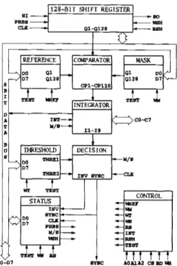
The correlator is basically composed of shift, reference, mask, status, threshold registers, a comparator, an integrator, a decision maker and a controller. Figure 1 shows the block diagram of the correlator. The controller controls all the 1 / 0 operations and the internal clocking in the chip. The shift reg- ister shifts the data from serial data input (SI) to serial data output (SO) and holds the 128 consecutive data bits for corre- lation. The reference 2nd mask re 'sters are 128-bit write-only registers containing eight 16-bit sfift registers. The reference
5 - 1 4 6 CH2704-5/89/0000/5146/$01 .OO
0
1989 IEEEregister is loaded with the sync word and the mask register is loaded with mask data. Logic 1's in the mask register masks the corresponding bits in the 128-bit shift register. The error toler- ances for both inverted and non-inverted sync words are stored in the threshold register which is composed of eight 2-bit shift registers. Through the status register, a p P reads the states of certain internal signals and controls the chip operation for 128
or 256-bit correlation and PRBS generation.
Correlation starts in the 128-bit comparator which com- pares the bits in the shift and reference registers and produces a logic 1 for each matched bit. The mask register's logic 1 outputs force the corresponding outputs of the comparator to logic 1, irrespective of the logic levels of shift and reference register con- tents. The integrator simply counts the matched and masked bits at the output of the comparator and feeds this information to the decision maker. The decision maker uses the integra- tor output and the error tolerances in the threshold register to decide whether the sync word is detected or not. For 256-bit correlation, two chips are cascaded in a master-slave configura- tion. The slave chip sends its integrator output to the master chip and the integrator outputs of both chips are added using an 8-bit adder in the master chip.
an 0 1 - 0 1 2 8
I
REFERENCE COMPARATOR MASK
DO 01 a1 DO D7 0128- 0128 D 7 k 1FE- C 0 - m 11-19
a
THRESHOLD DECISION + w e I l p v S l l o C--
DO-'-
D7 -2-t
t
WE TEST 7A p P can access all the registers in the chip through 8-bit data and 3-bit address bus. Shift, reference and mask registers are loaded by 8-bit wide serial data in 16 write cycles. Similarly, the threshold register is loaded in 2 write cycles. The pP can read the most significant 8-bit of the shift register, 8-bit integra- tor output and three bits of the status register. It can change the reference sync word data, mask data and the threshold data dynamically. The p P is informed on the sync word detection either by an interrupt signal or by polling.
While designing the correlator chip, some “ad hoc de- sign for testability” methods are used; control and observation switching, in amplification, blocking or degating logic for par- titioning [1[[2]. In addition, the scan design technique is applied such that, in the test mode (when test signal is high), the ref- erence, mask, threshold, and status registers are connected in such a way that they form a single shift register which we call as scan path. Since the number of pins available for test purposes is minimal, the number of test pins is increased by multiplex- ing of the normal output pins to perform an additional function of acting as test outputs. For blocking or degating, additional gates are incorporated into the design to inhibit data flow along the paths, thus partitioning the circuit into smaller modules for the purpose of testing. The test patterns are generated using an automatic test pattern generator by means of path sensitization technique and only stuck-at faults are taken into consideration in relation with the chip layout [2],[3]. The register blocks are instrumental in applying the test inputs to other modules, thus the registers has to be tested first for possible faults before test- ing could begin on combinational subcircuits. The tests per- formed on the registers comprise a “flush” and a “shift” test; that is, clocking a pattern 001100, which checks all combina- tions of initial and next states through the registers, which can be concatenated into a single serial shift register. The compara- tor and integrator blocks are exhaustively tested with approxi- mately 6000 test vectors by sensitizing independent paths from the layout. Consequently, as a result of the partitioned test- ing, the number of test patterns are reduced significantly that makes the fault simulation easier and faster. The testability is considerably improved by a 2 % increase in the overall transistor count.
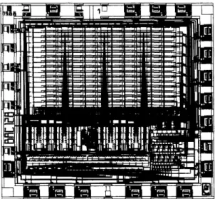
In the layout design of the chip, VLSI complexity is re- duced by the construction of a hierarchical layout. The routing of the comparator, shift, reference and mask registers became a serious problem which might not be solved if gate arrays or stan- dard cells were used in the layout design. This routing problem is solved by merging the shift, reference and mask registers and the comparator in a single cell then by constructing an 8x16 array structure from these cells. The cells in the array are ar- ranged for the loading of the registers so that the array occupies the minimum area. The integrator is constructed from adders connected in the form of an inverse binary tree in 7-levels. The i- th level (i=O
...
6) contains 2(’-’) i-bit adders. Since these adders are found in a binary tree form, the gate count at the sum and carry sta es of each adder is reduced, and a considerable area and speei are improved. All primitive cells are designed at the transistor level and complementary static CMOS logic style is used in these cells. In the chip, twc-phase clocking is used. Two phase clock is generated and drived by local clock drivers. The clocks are distributed with the metal lines in equal lengths for both phases.The layout of the chip is drawn and its netlist is extracted by using the Magic layout editor on SUN workstations. The simulations are performed at all levels of the layout hierarchy. The Spice and Esim simulators are used for simulating the small sized cells and more com licated cells, respectively. The layout of the chip is plotted in 2.
Total area Device count Maximum freauencv
Chip characteristics
5.6mmx5.2” 15,000 transistors lMHz istics are given in table 1.Pin count
Technolom
I
3um n-well MZCMOSI
28I
Active area1
4mmx4.3”1
I
MaximumDowerI
80mW @1MHzI
Table 1: The Chip characteristics.
Acknowledgement
N. Aral and T. Ergiin of ASELSAN made most of the system design of the correlator. This research was sponsored by NATO’s Scientific Affairs Division in the framework of the Science for Stability Programme.
Figure 2: Tlic l a p i i t of thc corrclator.
References
[l] T. W. Williams and K. P. Parker, “Design For Testability-A Survey”,
mIEEE,
vol. 71, pp. 98-112, Jan. 1983. 21 G. Russell, D. J. Kinniment, E. G. Chester, M. R. McLauh-I,
,
CAD for VLSI. England, Van Nostrand Reinhold, 1985. [3] J. A. Abraham and W. K: Fuchs, “Fault and Error Mod- els for VLSI”, Proc. IEEE, vol. 74, pp. 639-654, May 1986.The 128-bit correlator chip is ready for fabrication in 3 micron double metal CMOS technology. According on the sim- ulation results, the chip can make correlation at lMbps rate with a power dissipation less than 80mW. The chip character-
5