Controlled photoluminescence in amorphous-silicon-nitride microcavities
Ali Serpengüzel, and Selim Tanriseven
Citation: Appl. Phys. Lett. 78, 1388 (2001); doi: 10.1063/1.1347022 View online: https://doi.org/10.1063/1.1347022
View Table of Contents: http://aip.scitation.org/toc/apl/78/10
Published by the American Institute of Physics
Articles you may be interested in
Photoluminescence of Si-rich silicon nitride: Defect-related states and silicon nanoclusters
Applied Physics Letters 90, 131903 (2007); 10.1063/1.2717014
Photoluminescence from silicon nitride—no quantum effect
Journal of Applied Physics 110, 023520 (2011); 10.1063/1.3607975
Emission properties of high- silicon nitride photonic crystal heterostructure cavities
Applied Physics Letters 93, 021112 (2008); 10.1063/1.2958346
Gap states in silicon nitride
Applied Physics Letters 44, 415 (1984); 10.1063/1.94794
Investigation of charge trapping centers in silicon nitride films with a laser-microwave photoconductive method
Applied Physics Letters 62, 615 (1993); 10.1063/1.108873
Microstructure and properties of silicon nitride thin films deposited by reactive bias magnetron sputtering
Controlled photoluminescence in amorphous-silicon-nitride microcavities
Ali Serpengu¨zela)
Physics Department, Koc¸ University, Sariyer, Istanbul 80910, Turkey Selim Tanriseven
Physics Department, Bilkent University, Bilkent, Ankara 06533, Turkey
共Received 23 August 2000; accepted for publication 12 December 2000兲
Narrow-band and enhanced photoluminescence have been observed in hydrogenated amorphous-silicon-nitride microcavities. The distributed Bragg reflectors were fabricated using alternating layers of hydrogenated amorphous-silicon nitride and hydrogenated amorphous-silicon oxide. The microcavity resonance wavelength was designed to be at the maximum of the bulk hydrogenated amorphous-silicon-nitride luminescence spectrum. At the microcavity resonance, the photoluminescence amplitude is enhanced, while the photoluminescence linewidth is reduced with respect to the bulk hydrogenated amorphous-silicon nitride. © 2001 American Institute of Physics. 关DOI: 10.1063/1.1347022兴
The ability to control the emission properties of semi-conductors with optical microcavities and photonic band-gap materials is continuing to attract the attention of the photon-ics community.1 As they alter the properties of the optical gain media, optical microcavities can be used in very low-threshold lasers and very efficient light-emitting diodes 共LEDs兲.2
Optical microcavities have also been applied to porous silicon共-Si兲, after the observation of room-temperature vis-ible photoluminescence 共PL兲 made -Si a potential optical gain medium.3 Microcavity-controlled PL in-Si has been observed experimentally4 and calculated theoretically.5 Microcavity-controlled electroluminescence共EL兲 of-Si has also been reported.6 Optical waveguides have been formed from -Si,7 and two-dimensional photonic crystals have been fabricated in-Si optical waveguides.8
Similar to -Si, hydrogenated amorphous silicon (a-Si:H) also exhibits room-temperature visible PL.9 In ad-dition, planar waveguides are being realized from a-Si:H.10 An advantage of a-Si:H is that it can be deposited by plasma-enhanced chemical-vapor deposition共PECVD兲 on al-most any substrate at temperatures below 500 K, which makes it potentially compatible with microelectronic tech-nology. These developments justify the renewed interest in silicon共Si兲 as a potential optoelectronic material. With mod-ern process techniques, it will be possible to integrate lasers, photodetectors, and waveguides into optoelectronic Si motherboards.11
Recently, we have observed room-temperature visible PL from a-Si:H nitride (a-SiNx:H).12 The efficiency of the PL from a-SiNx:H is approximately 3%, which agrees well with previously published results for a-Si:H.13We have also observed the enhancement of PL in a planar a-SiNx:H mi-crocavity realized with metallic mirrors.14 While the exact mechanism of the occurrence of the PL in bulk a-SiNx:H is still under discussion, we have suggested12 the use of a quantum-confinement model.15 There, it was proposed that
our samples consist of small a-Si clusters in a matrix of a-SiNx:H. The regions with Si–H and Si–N, having larger energy gaps due to strong Si–H and Si–N bonds, isolate these a-Si clusters, and form barrier regions around them. The PL originates from the a-Si clusters.
In this letter, we report the control of PL in an all-dielectric a-SiNx:H microcavity. The microcavity is realized by sandwiching the active a-SiNx:H layer between two dis-tributed Bragg reflectors共DBRs兲. The microcavity resonance wavelength was designed to be at the maximum共710 nm兲 of the bulk a-SiNx:H luminescence spectrum.
The microcavity was realized by a/2 active 共i.e., lumi-nescing兲 layer of a-SiNx:H sandwiched between two passive DBR mirrors. As found in our previous studies, the presence of the ammonia (NH3) in growth determines whether the a-SiNx:H will be active or passive. First, the passive bottom DBR was deposited by PECVD on the Si substrate using 14 pairs of /4 alternating layers of a-SiNx:H 共with refractive index⫽1.72 and metric thickness⫽104 ⫾5 nm兲 and a-SiOx:H 共with refractive index⫽1.45 and metric thickness⫽124⫾6 nm兲. For the passive a-SiNx:H deposition, ammonia (NH3) with a flow rate of 10 sccm, and
2% silane (SiH4) in nitrogen (N2) with a flow rate of 180
sccm were used. For the passive a-SiOx:H deposition, ni-trous oxide (N2O) with a flow rate of 25 sccm, and 2% SiH4 in N2 with a flow rate of 180 sccm were used. After the
deposition of the bottom DBR, a /2 layer of active a-SiNx:H 共with refractive index⫽2.03 and metric thickness ⫽163⫾8 nm兲 was deposited. For the active a-SiNx:H depo-sition, only 2% SiH4in N2with a flow rate of 180 sccm was
used. Afterwards, the top DBR was deposited, using 14 pairs of /4 alternating layers of a-SiOx:H and a-SiNx:H. The radio-frequency power was 20 W, and the deposition cham-ber pressure 1 Torr during the continuous deposition process. Figure 1 shows a schematic of the a-SiNx:H microcavity. The /4 passive a-SiNx:H layers are shown in black, while the/4 passive a-SiOx:H layers are shown in white. The/2 central layer of active a-SiNx:H is shown in gray.
Figure 2 shows the measured room-temperature reflec-tance 共upper curve兲 and PL 共lower curve兲 spectra of the a兲Author to whom correspondence should be addressed; electronic mail:
APPLIED PHYSICS LETTERS VOLUME 78, NUMBER 10 5 MARCH 2001
1388
a-SiNx:H microcavity. The room-temperature reflectance and PL measurements were made at 0°⫾5° with respect to the surface normal with a resolution of 0.1 nm. The PL spec-tra were later corrected for the responsivity of the spectrom-eter and the photomultiplier tube. An Ar⫹laser with a wave-length of 514.5 nm and a power of 150 mW was focused with a 15 cm focal length cylindrical lens on the samples. During the PL measurements the temperature of the sample is not controlled and there might be local heating, which reduces the PL efficiency and broadens the PL linewidth.16 However, local heating would not considerably affect the general shape and features of the a-SiNx:H gain spectrum. As seen in the PL spectra of Fig. 3, even though there might be local heating, we are observing strong PL from the sample.
There is good agreement between the reflectance and the PL spectra. Both the reflectance and the PL spectra of Fig. 2 show a microcavity resonance at a wavelength of 710 nm. This resonance has a linewidth of ⌬⫽6 nm and a quality factor of Q⫽118. The PL is enhanced by the microcavity resonance, which correlates well with the minimum of the reflectance spectrum.
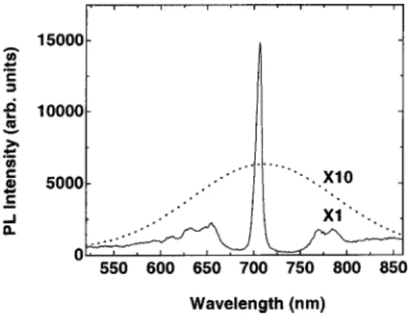
In order to clarify the effect of the microcavity and to demonstrate its advantages with respect to the bulk a-SiNx:H, we also show the PL of a/2-thick layer of bulk a-SiNx:H 共dotted line兲 in Fig. 3, obtained under the same experimental conditions. The red–near-infrared PL of the
bulk a-SiNx:H has a broad linewidth of 240 nm. This broad linewidth shows that a-SiNx:H has potential as a photonic gain medium.
A comparison of the spectra in Fig. 3 shows that the effect of the microcavity is twofold: first, the wide emission band 共240 nm兲 is strongly narrowed to 6 nm; second, the resonant enhancement of the peak PL intensity is more than one order of magnitude with respect to the emission of the /2-thick layer of bulk a-SiNx:H. In addition, by choosing the appropriate width of the a-SiNx:H active layer and DBRs, it is possible to select the emission wavelength of the microcavity by taking advantage of the broad spectral emis-sion of the a-SiNx:H active layer.
In conclusion, we have demonstrated that a-SiNx:H mi-crocavities with DBR mirrors can be successfully realized by PECVD, and can be used for the control of the PL in a-SiNx:H. The PL of the a-SiNx:H is both narrowed and enhanced at the microcavity resonance with respect to the PL of the bulk a-SiNx:H. This narrowing and enhancement of the PL can be understood by the redistribution of the density of optical modes due to the presence of the microcavity. The microcavity narrowing and enhancement of luminescence in a-SiNx:H opens up a variety of possibilities for optoelec-tronic applications such as resonant cavity enhanced LEDs.
The authors would like to acknowledge the partial sup-port of this research by the North Atlantic Treaty Organiza-tion 共NATO兲, Grant No. SfP-971970 and the Scientific and Technical Research Council of Turkey 共TUBITAK兲, Grant No. TBAG-1952.
1
Microcavities and Photonic Band Gaps: Physics and Applications, edited by J. Rarity and C. Weisbuch共Kluwer, Dordrecht, 1996兲.
2R. E. Slusher and C. Weisbuch, Solid State Commun. 92, 149共1994兲. 3T. Canham, Appl. Phys. Lett. 57, 1046共1990兲.
4L. Pavesi, C. Mazolleni, A. Tredicucci, and V. Pellegrini, Appl. Phys. Lett. 67, 3280共1995兲.
5E. K. Squire, P. St. J. Russell, and P. A. Snow, Appl. Opt. 37, 7107 共1998兲.
6M. Araki, H. Koyama, and N. Koshida, Appl. Phys. Lett. 69, 2956共1996兲. 7
H. F. Arrand, T. M. Benson, P. Sewell, and A. Loni, J. Lumin. 80, 199 共1999兲.
8S. W. Leonard, H. M. van Driel, K. Busch, S. John, A. Birner, A.-P. Li, F. Mu¨ller, U. Go¨sele, and V. Lehmann, Appl. Phys. Lett. 75, 3063共1999兲. 9D. J. Wolford, B. A. Scoot, J. A. Reimer, and J. A. Bradley, Physica B
117, 920共1983兲.
10A. M. Agarwal, L. Liao, J. S. Foresi, M. R. Black, X. Duan, and L. C. Kimerling, J. Appl. Phys. 80, 6120共1996兲.
FIG. 1. Schematic of the a-SiNx:H microcavity with DBR mirrors.
FIG. 2. Experimental reflectance共upper curve兲 and PL 共lower curve兲 spec-trum of the a-SiNx:H microcavity.
FIG. 3. 1⫻PL spectrum of the /2 a-SiNx:H microcavity共solid line兲 and
10⫻PL spectrum of the /2 bulk a-SiNx:H共dotted line兲.
1389
11A. Kaneko, T. Goh, H. Yamada, T. Tanaka, and I. Ogawa, IEEE J. Sel. Top. Quantum Electron. 5, 1227共1999兲.
12A. Aydinli, A. Serpengu¨zel, and D. Vardar, Solid State Commun. 98, 273 共1996兲.
13
D. J. Wolford, B. A. Scott, J. A. Reimer, and J. A. Bradley, Physica B
117B&118B, 920共1983兲.
14A. Serpengu¨zel, A. Aydinli, A. Bek, and M. Gu¨re, J. Opt. Soc. Am. B 15, 2706共1998兲.
15M. H. Brodsky, Solid State Commun. 36, 55共1980兲.
16R. Fisher, in Amorphous Semiconductors, edited by M. H. Brodsky 共Springer, Berlin, 1985兲, pp. 159–187.