1
Novel Nanocomposite Coatings of Nanoparticles
A THESIS
SUBMITTED TO THE DEPARTMENT OF MATERIALS SCIENCE AND NANOTECHNOLOGY
AND THE GRADUATE SCHOOL OF ENGINEERING AND SCIENCE OF BILKENT UNIVERSITY
IN PARTIAL FULLFILMENT OF THE REQUIREMENTS FOR THE DEGREE OF
MASTER OF SCIENCE
By
Refik Sina Toru
April 2011
2
I certify that I have read this thesis and that in my opinion it is fully adequate, in scope and in quality, as a thesis for the degree of Master of Science.
Assoc. Prof. Dr. Hilmi Volkan Demir (Supervisor)
I certify that I have read this thesis and that in my opinion it is fully adequate, in scope and in quality, as a thesis for the degree of Master of Science.
Assoc. Prof. Dr. Dönüş Tuncel
I certify that I have read this thesis and that in my opinion it is fully adequate, in scope and in quality, as a thesis for the degree of Master of Science.
Assist. Prof. Dr. Ali Kemal Okyay
Approved for the Institute of Engineering and Science:
Prof. Dr. Levent Onural
3
ABSTRACT
NOVEL NANOCOMPOSITE
COATINGS OF NANOPARTICLES
Refik Sina Toru
M.S. in Materials Science and Nanotechnology
Supervisor: Assoc. Prof. Dr. Hilmi Volkan Demir
April 2011
Incorporating nanoparticles into nanocomposite thin-films enables coatings with multi-functionality depending on the particle type and size, and the film morphology. These multiple functions may include, for example, combinations of photocatalysis, hydrophobicity, scratch resistance, and antibacterial property. Here we proposed and demonstrated a new encapsulation nanocomposite with controllable refractive index and potentially additional functional properties for coating photonic devices, for instance, light-emitting diodes (LEDs). To design and implement this nanocomposite coating with tunable refractive index, we employed TiO2 nanoparticles of various diameters because of their relatively
high refractive index. We embedded these nanoparticles in our encapsulation sol-gel material during synthesis. In addition, we incorporated several polymer-forming chemicals during synthesis to control additional functions such as hydrophobicity and scratch resistance. We used characterization tools of atomic force microscopy, refractometry, contact angle measurement, and scanning electron microscopy to study material properties.
4
ÖZET
YENİLİKÇİ NANOPARÇACIK İÇEREN
NANOKOMPOZİT KAPLAMALAR
Refik Sina Toru
Malzeme Bilimi ve Nanoteknoloji Bölümü Yüksek Lisans Tez Yöneticisi: Doç. Dr. Hilmi Volkan Demir
Nisan 2011
Nanoparçacıklar katılarak oluşturulan nanokompozit ince filmler, katkıların tip ve boyutlarına ve ayrıca yüzey morfolojisine bağlı olarak çok fonksiyonlu yüzeylerin oluşturulmasını sağlar. Çok fonksiyonluluk; fotokataliz, su iticilik, çizilme dayanımı, antibakteriyellik gibi özelliklerin aynı anda bir yüzeyde bulunmasıdır. Bu tez çalışmasında; ışık veren diyot (LED) ve benzeri fotonik cihazlar için, kontrol edilebilir kırılma indeksine ve ek fonksiyon potansiyeline sahip olan yeni bir kaplama malzemesi önerilmiş ve gösterilmiştir. Bu ayarlanabilir kırılma indeksine sahip olan nanokompozit kaplamayı tasarlamak ve uygulamak için çeşitli çaplara sahip olan TiO2 nanoparçacıklar seçildi. TiO2
parçacıklar göreceli olarak yüksek olan kırılma indeksleri sebebi ile seçildiler. Nanoparçacıklar sentez esnasında kaplama malzememiz olan sol-jel meskenin içine yerleştirildi. Ek olarak, çeşitli polimer oluşturucular kullanılarak sentez esnasında su iticilik, çizilme dayanımı gibi fonksiyonlar bu kaplama malzemelerine kazandırıldı. Hazırlanan kaplama malzemelerinin özellikleri, atomik kuvvet mikroskobu, refraktometre, temas açısı ölçer ve tarama elektron mikroskobu ile incelendi.
5
Acknowledgements
I would like to express my deepest appreciation to my advisor, Assoc. Prof. Dr. Hilmi Volkan Demir for his motivation and guidance during my research in Bilkent University.
I would also like to thank my committee members Assoc. Prof. Dr. Dönüş Tuncel and Assist. Prof. Ali Kemal Okyay for their valuable comments and suggestions.
I would also like to thank to our research partners Gülsen Çeliker, Dr. Hüseyin Çeliker and Selahattin Yılmaz from Innovcoat, for sharing their knowledge on sol-gel technique, useful discussions and their hospitality during my visits to Innovcoat in Gebze.
I would also like to thank to Prof. Dr. Salim Çıracı for the facilities used in National Nanotechnology Research Center (UNAM) during research. I would also like to thank staff of UNAM for their help.
I would like to extend my thanks to members of devices and sensors group for their support on both technical matters and their friendship.
My greatest gratitude goes to all my family: my parents, my grandparents, my uncle and aunts, for their patience and support during my research and while I was writing my thesis.
6
Table of Contents
1. INTRODUCTION ... 10
2. REVIEW OF NANOPARTICLES FOR PHOTOCATALYSIS ... 12
2.1PHOTOCATALYSIS ... 13
3. STATE-OF-THE-ART COATINGS FOR PHOTONIC DEVICES ... 15
3.1DESIRED PROPERTIES OF ENCAPSULATION COATINGS ... 17
3.2COMMONLY USED ENCAPSULATION COATINGS ... 18
3.2.1EPOXY RESIN ... 18
3.2.2SILICONE ... 19
3.2.3POLYMETHYL METHACRYLATE (PMMA) ... 21
4. NANOCOMPOSITE COATINGS FOR DIFFERENT FUNCTIONS ... 22
4.1LIGHT EXTRACTION FUNCTION ... 22
4.1.1REFRACTIVE INDEX AND ITS EFFECT ON EFFICIENCY ... 22
4.1.2TRANSPARENCY ... 24
4.2SUPPORTING FUNCTIONS ... 25
4.2.2HIGH TEMPERATURE RESISTANCE ... 25
4.2.3MECHANICAL PROPERTIES ... 26
4.2.4MOISTURE ABSORBTION AND HERMETICITY ... 27
4.2.5PHOTOCATALYSIS ... 28
5. METHODOLOGY ... 29
5.1LÉVY GLASS ... 29
5.2NANOSIZED PARTICLE SELECTION ... 31
5.3SYNTHESIS OF ENCAPSULATION MATERIAL ... 31
5.3.1SOL-GEL TECHNIQUE ... 31
5.3.2MATERIALS USED IN SYNTHESIS ... 32
5.3.3SYNTHESIS SETUP ... 33
6. PARAMETRICAL STUDY AND RESULTS ... 35
6.1EFFECTS OF VARIOUS POLYMER FORMERS ... 35
6.1.1EFFECT OF APTES ON ENCAPSULATION MATERIAL ... 36
6.1.2EFFECTS OF VTMO ON ENCAPSULATION MATERIAL ... 41
6.2EFFECTS OF TIO2SIZE AND CONCENTRATION ... 47
6.2.1RESULTS OF 6NM SAMPLES ... 47
6.2.2RESULTS OF 240 NM SAMPLES ... 49
6.2.3RESULTS OF 6 NM AND 240 NM COMBINED SAMPLES ... 51
6.2.4RESULTS OF REFRACTIVE INDEX MEASUREMENTS ... 56
6.2.4RESULTS OF TRANSPARENCY AND ABSORPTION MEASUREMENTS ... 62
7
List of Figures
Figure 1. Photocatalysis [24] ... 14
Figure 2. Light Escape Cone- Ref:High power LED arrays [26] ... 16
Figure 3. Position of encapsulation material within the LED [27]... 17
Figure 4. Various epoxy curing paths [31]. ... 19
Figure 5. Degree of organic substitution in silicone [33]. ... 20
Figure 6. Transparency change of silicone under exposure to 200oC for various time intervals [28]. ... 21
Figure 7. Effect of temperature on lifetime of LEDs [37]. ... 26
Figure 8. Stress-strain diagram of brittle material vs. ductile material. ... 27
Figure 9. Schematic of photocatalysis. ... 28
Figure 10. a) Normal diffusion (Brownian) b) random walk process (Lévy flight) [45]. ... 30
Figure 11. Monte Carlo simulation of a Lévy flight material [45]. ... 30
Figure 12. Our setup used for synthesizing sol-gel composites at UNAM. ... 34
Figure 13. Effect of APTES concentration on refractive index. ... 36
Figure 14. APTES-1 12µm. ... 37 Figure 15. APTES-1 3 µm. ... 37 Figure 16. APTES-2 12 µm. ... 38 Figure 17. APTES-2 3 µm ... 38 Figure 18. APTES-3 12 µm. ... 39 Figure 19. APTES-3 3 µm. ... 39
Figure 20. APTES-1 contact angle measurement showing hydrophobicity... 40
Figure 21. APTES-2 contact angle measurement showing hydrophobicity... 40
Figure 22. APTES-3 contact angle measurement showing hydrophobicity... 40
Figure 23. Effect of increase of VTMO ratio on refractive index. ... 41
Figure 24. VTMO-1 12 µm. ... 42 Figure 25. VTMO-1 3 µm. ... 43 Figure 26. VTMO-2 12 µm. ... 43 Figure 27. VTMO-2 3 µm. ... 44 Figure 28. VTMO-3 12 µm. ... 44 Figure 29. VTMO-3 3 µm. ... 45
Figure 30. VTMO-1 Contact angle measurement showing hydrophobicity. ... 46
Figure 31. VTMO-2 Contact angle measurement showing hydrophobicity. ... 46
Figure 32. VTMO-3 Contact angle measurement showing hydrophobicity. ... 46
Figure 33. 6nm TiO2 particles, SEM measurement on 100 µm scale using under loaded recipe. ... 48
Figure 34. 6nm TiO2 Particles, SEM measurement on 100 µm scale using original recipe. ... 48
Figure 35. 6 nm TiO2 Particles, SEM measurement on a 100 µm scale using overloaded recipe. ... 49
8
Figure 36. 240 nm TiO2 particles, SEM measurement on a 100 µm scale using
under loaded recipe. ... 50
Figure 37. 240nm TiO2 particles, SEM measurement on 100 µm scale using original recipe. ... 50
Figure 38. 240 nm TiO2 particles, SEM measurement on a 100 µm scale using over-loaded recipe. ... 51
Figure 39. SEM measurement of under-loaded 6 nm and 240 nm sample (100 µm scale). ... 52
Figure 40. SEM measurement of original recipe 6 nm and 240 nm sample (100µm scale). ... 52
Figure 41. SEM measurement of over-loaded 6 nm and 240 nm sample (100 µm scale). ... 53
Figure 42. SEM of under-loaded 6 nm and over loaded 240nm sample, (100µm scale). ... 53
Figure 43. SEM of over-loaded 6 nm and under loaded 240 nm sample (100µm scale). ... 54
Figure 44. SEM of under-loaded 6 nm and original 240 nm sample (100µm scale). ... 54
Figure 45. SEM of over-loaded 6 nm and original 240 nm sample (100µm scale). ... 55
Figure 46. SEM of original 6 nm and under-loaded 240 nm sample (100µm scale). ... 55
Figure 47. SEM of original 6 nm and over-loaded 240 nm sample (100µm scale). ... 56
Figure 48. Effect of concentration on the refractive index for 6 nm TiO2 particle. ... 57
Figure 49. Effect of concentration on the refractive index for 240 nm TiO2 particle. ... 58
Figure 50. Effect of combining different sized TiO2 by using original recipe. .. 59
Figure 51. Effect of combining different sized TiO2 on low concentration. ... 60
Figure 52. Effect of combining different sized TiO2 in high concentration. ... 61
Figure 53. Effect of concentration on refractive index of combo materials. ... 61
Figure 54. Absorption results for 6 nm particle samples. ... 62
Figure 55. Absorption results for 240 nm particle samples. ... 63
Figure 56. Transparency results for 6 nm particle samples. ... 64
9
List of Tables
Table 1. Refractive indices of various semi-conductors. ... 23 Table 2. Critical angles for various semi-conductor materials ... 24 Table 3. Effect of high refractive index medium on reflection ... 24
10
Chapter 1
Introduction
Light-emitting diodes (LEDs) have been invented by Dr. Nick Holonyak, Jr. and companies in 1960s [1]. Since the invention of LEDs, numerous research groups and companies have worked on increasing their performance as well as making them affordable and reliable. One way of improving LED’s performance is to improve their photon extraction and thus encapsulation. Semiconductor materials of LEDs where photons are generated exhibit relatively high refractive indices when compared with that of air. This refractive index difference results in total internal reflection generating a small photon escape cone, and therefore reducing photon extraction of the LED. Increasing efficiency of LED is thus possible by creating an intermediate medium between air and semiconductor core with a refractive index between them. This medium may serve as encapsulation. The encapsulation material does not only act as a light path to increase light extraction efficiency, but also may provide additional features including better packaging.
In this thesis, we proposed and further demonstrated a coating which may potentially provide additional functional properties. To design and implement this material with possibly tunable refractive index, we have employed TiO2
nanoparticles of various diameters because of their high refractive index. We embedded TiO2 nanoparticles in our encapsulation material during sol-gel
synthesis, which we have developed with our partner Innovcoat. In addition to TiO2 embedding, we also incorporated several polymer forming chemicals
during synthesis to control additional functions including hydrophobicity and scratch resistance. We used characterization tools of atomic force microscopy,
11
ellipsometry, contact angle measurement and scanning electron microscopy to inspect material properties.
The rest of thesis is organized as follows. In the second chapter, desired properties expected from encapsulation materials and the properties of currently commercially available encapsulation materials are explained. In the third chapter, the discussion on various functions is broadened. In fourth chapter, our methodology is introduced, including the discussion of Lévy glass, nano sized additives and their effects, our starting recipe and modifications we made on it. In the fifth chapter, the experimental results of our parametrical studies will be presented and discussed. In the sixth chapter various functions will be demonstrated in our experimental sets. Finally, in the seventh chapter, the results
12
Chapter 2
Review of Nanoparticles for
Photocatalysis
Metal oxide induced photocatalysis had been widely investigarted over the last three decades [2-4]. Various metal oxides had been shown to have photocatalytic effects, including but not limited to TiO2, CdS, ZnS, ZnO, WO3, SrTiO3,
α-Fe2O3, V2O5, Ag2O [5-6]. Photocatalytic effect enables abundant applications
such as; water splitting [5-6], oxidation of organic pollutants [7], removal of inorganic pollutants [8], photocatalytic destruction of gaseous organic pollutants [9], photodynamic therapy and photodisinfection [10], photoelectrochemical cells for electricity production [11], photodissocation of water, sensitizers for organic photosynthetic processes [12] and photoreduction of N2 and CO2 [13-14]. In
addition to previously mentioned applications it had also been mentioned that photocatalytic material systems can also be applied to solar cells, chemical sensors, photoelectrochemical cells, and electronic devices for increased performance [15-16]. Properties of the metal oxide photocatalysts have a wide range, material crystalline and electronic structures with a number of oxidation states, possible coordination numbers, degrees of symmetry, ligand-field stabilization, and acid–base properties, the control of which yield compounds exhibiting insulating, semiconducting, conducting, or magnetic behavior with transitions between these states, differ for each material system [17]. Variety of the applications is related to this wide range of properties.
Among the semiconductor nanoparticles mentioned above, TiO2 is the one that
have been investigated most commonly; several review articles already cover this material [3, 4, 18]. The reason for such an interest in TiO2 nanoparticles is related
13
Photocatalysis have been investigated in aqueous environment very extensively but to use photocatalytic particles in devices, metal oxide particles are needed to be embeded into thin films. On the other hand, immobilization is predicted to reduce the catalyst surface and decrease the photocatalytic efficiency [19-20]. In a comparative study of photocatalytic efficiency in different forms of titanium dioxide have been compared. Among the forms of slurry, coating (by sputtering), sol-gel, and inorganic fiber, it has been found that the slurry form has the highest efficiency [21]. It has been suggested that the reason for the decreased efficiency in immobilized form is the reduction of active surface, introduction of ionic specimen, which causes recombination, and the difficulty of ion exchange [22]. Therefore, the main concern in immobilization of nanocatalysts is the reduced photocatalytic activity [23]. Consequently, research efforts to immobilize photocatalytic semiconductor particles while maintaining high photocatalytic efficiency are of great importance for future device applications.
2.1 Photocatalysis
Photocatalysis can be defined as increasing the rate of photoreactions by using optical activation. Photons energy is utilized by using metal-oxides as catalysts.
Process of photocatalysis has been demonstrated in Figure 1 in detail. Photocatalysis starts when the material system is optically excited by a photon, which has energy hν equal to or larger than bandgap energy (Eg) of the material
system. Excitation energy of the photon causes electron to make a transition from the valence band to the conduction band and leave a hole in the valence band.
This photogenerated electron-hole pair either recombines in the volume or diffuses to the surface, recombination means loss of the pair, which is not desired.
14
surface or initiate a chain of redox reactions. When the electron-hole pairs initiate
Figure 1. Photocatalysis [24]
redox reactions, H+, OH-, H2O2 and O2- species are supplied to environment.
Those species enable degradation of the contaminants. Recombination is the major mechanism causes efficiency to decrease in photocatalysis. Photocatalytic reaction efficiency relies on the fraction of the electron-hole pairs that contribute go in to the chain reaction instead of recombination. When photocatalysts are immobilized in thin films, their efficiency decreases significantly due to lower surface/volume ratio and hence higher recombination. In order to use them in devices, immobilization of the metaloxide catalysts is an obligation. Therefore, methods such as combining different metaloxides, adding dopants have been employed to increase the efficiency of the films.
15
Chapter 3
State-of-the-Art Coatings for
Photonic Devices
Packaging is one of the most essential parts of LEDs. Packaging is critically important because it provides LEDs with three important features: an electrical connection to provide driving power; a thermal connection to drive away excessive heat; and a transparent encapsulation to protect the chip and outcouple the generated light [25]. The electrical connection that carries the electrical input power is required to make an LED work, while the thermal connection is necessary for removing heat generated on the chip to prevent LED operation from failing or degrading due to excessive heat. On the other hand, transparent encapsulation protects the chip from environment and modifies light extraction. Generally, encapsulation materials are chosen among polymers, which typically have a refractive index varying from 1.5 to 1.8 [25]. Refractive index of the encapsulation material determines the angle of total internal reflection, and hence, the light cone, through which the generated photons are capable of escaping from LED semiconductor into air.
16
Figure 2. Light Escape Cone- Ref:High power LED arrays [26]
The light escape cone, shown in Figure 1, grows bigger and the resulting efficiency of light extraction increases with the decreasing refractive index contrast between the encapsulation material and LED chip [25]. In addition to light extraction modification, encapsulation materials available at the market may provide additional properties including chemical inertness, high-temperature stability, and hermetical sealing [25]. In this section, we describe the properties of such commercially available and commonly used encapsulating materials as well as their chemical structures and methods so far adapted to improve their performance.
17
Figure 3. Position of encapsulation material within the LED [27]
3.1 Desired Properties of Encapsulation Coatings
Encapsulation materials are required to feature various properties to ensure that LEDs are working properly. High transparency and high refractive index in UV-visible region, non-discoloring behavior when exposed to UV, chemical stability, high temperature stability, stable thermo-mechanical properties, low moisture absorption, and hermetical sealing are among the properties desired for encapsulation materials [25], [28].High transparency is mandatory for the encapsulation materials due to fact that encapsulation material not only protects semiconductor chip but also serves as a light way. Transparency of the encapsulation material must be sustained during entire device lifetime [28]. High refractive index is required for the encapsulation material to minimize outcoupling losses due to total internal reflection [28]. Typical semiconductors used in LEDs have refractive indices varying from 2.5 to 4.0 [25]. The refractive index of an ideal LED coating material should therefore be high enough so that photon extraction efficiency from the semiconductor would be efficient.
18
The process of yellowing (discoloring), which indicates the loss of optical transparency due to exposure to UV light or high temperatures, is one of the major problems occurring in the encapsulating materials [25]. LEDs are ideally expected to work for around 100,000 hours without failure under UV light exposure and at temperatures above 125⁰C. So the encapsulation material should be resilient to these conditions [26]. In addition, the encapsulation material should be stable enough to uphold mechanical effects such as stress and scratching. Finally, the semiconductor chip of an LED is needed to be protected against moisture and oxygen to prevent failure in long term; therefore the encapsulation material should have low moisture absorption and be highly hermetical.
3.2 Commonly Used Encapsulation Coatings
3.2.1 Epoxy Resin
Epoxy is a commonly used encapsulation coating. Epoxy is a thermosetting polymer, which is produced by the reaction of a resin and a hardener. Epoxy compositions commonly used in LEDs are cured either directly thermally or by using UV light [29]. Epoxy resin refractive index is typically around 1.6 [25]. The advantages of using thermosetting epoxy are also related to its properties such as chemical resistance, electrical insulation, mechanical resistance and relative thermal stability. Moreover, epoxy resins can also be tailored according to specific needs by altering starting resins and using different curing systems [30]. Several of curing paths are demonstrated in Figure 3. All of the curing paths given in Figure 3 causes final epoxy to have different properties. Some of the combinations are good as adhesives; some of them are good for encapsulation.
19
Figure 4. Various epoxy curing paths [31].
However, due to related disadvantages including the reduced optical transparency as a result of exposure to ultraviolet light prolonged exposure to temperatures above 120⁰C, other encapsulation materials have been searched [32].
3.2.2 Silicone
Silicone polymers have been used as optical lenses, mechanical stress relieving encapsulation materials, and light path materials in LEDs [28]. Silicone is a quiet attractive encapsulation material owing to its high transparency in the visible spectrum and versatility of its refractive index [28]. The refractive index of commercially available silicone materials varies between 1.38 and 1.55, and the refractive indexes up to 1.7 are achieved experimentally [28]. In addition to its good optical properties, silicone also exhibits stable thermo-mechanical properties. It does not yellow (discolor) under high UV illumination and is resilient to humidity [30].
20
Figure 5. Degree of organic substitution in silicone [33].
Degree of organic substitution affects properties of the silicone chain. If organic compounds are added into the chemical structure instead of oxygen, silica glass turns into silicone polymer, which is soft and flexible, suitable for encapsulation applications. Figure 4 explains property modification of silicone with additives. In Figure 4, Q-type is the silica (glass) form, which is brittle and only consists of oxygen in addition to Si. T-type substitutes one oxygen with a organic compound and forms silicone resin. In case of D-type, two of the oxygen atoms are substituted with radical groups, which cause silicone to form long chains. Radical group can be methyl, phenyl, or any other organic groups. Type of the radical group affects the refractive index of the final silicone compound. Ratio of phenyl in silicone compound is highly used to tailor its refractive index [33].
Thermal stability of the silicone is also superior to other encapsulation materials. Figure 5 shows effect of exposure to 200oC over time (which is even more severe than the normal operational condition of LEDs, which is around 125oC). As can be seen in Figure 5, exposure to 200oC decreases the optical transparency in the
21
UV region (below 390 nm), although in the visible and infrared region (above 390 nm), there is no significant transparency loss [28].
Figure 6. Transparency change of silicone under exposure to 200oC for various time
intervals [28].
Because of its optical properties such as transparency and relatively high refractive index and stable thermo-mechanical properties, silicone is currently the most widely used encapsulation material chosen for the optical and electronic devices.
3.2.3 Polymethyl methacrylate (PMMA)
Polymethyl methacrylate (PMMA) is a thermoplastic, optically transparent material. PMMA is also comerically known as acrylic glass or plexiglas. PMMA is formed by combining monomers with chemical reactions. PMMA is less favored as an encapsulation material for having relatively low refractive index. PMMA’s refractive index is 1.49 [34]. Even after embedding TiO2 into the
material to enhance its refractive index, it only goes up to 1.55 [35]. In addition to its low refractive index, it is also a brittle material, which makes it mechanically less desirable [36]. On the other hand, PMMA is cheaper to produce; therefore, it had been used as a encapsulation material in some applications. But, due to its weak mechanical performance and low refractive index, its applications have been limited.
22
Chapter 4
Nanocomposite Coatings for
Different Functions
LED encapsulation materials are desired to exhibit several functions, which can be divided into two categories: light extraction function and supporting functions. Light extraction function, which relies on refractive index and transparency of the medium, is one of the main traits that affect LED performance directly. Other functions including non-discoloring property when exposed to UV, chemical stability, high temperature stability, stable thermo-mechanical properties, low moisture absorption, and being hermetical are among the supporting functions that increase lifetime of LEDs. These therefore make LEDs more reliable. In this chapter, first light extraction function will be discussed in detail, following which supporting functions will be explained.
4.1 Light Extraction Function
LED’s light extraction efficiency is directly related to transparency and refractive index of the encapsulation material. Additives with high reflective indices increase the refractive index of the encapsulation material, thus increasing extraction efficiency. On the other hand such additives also cause optical transparency of the encapsulation material to decrease. Due to this trade-off, optimization is required to achieve the best possible performance.
4.1.1 Refractive index and its effect on efficiency
Effect of refractive index on efficiency can be explained by two inter-related mechanics: total internal reflection and transmission/reflection coefficients. Total internal reflection causes photons emitted from the semiconductor core to be
23
trapped within the core, and, therefore, decreases extraction efficiency. Total internal reflection occurs when a photon travelling from a higher refractive index medium to a lower refractive index medium hits the boundary with at an angle larger than the so-called critical angle, øc. Refractive indices of several commonly
used core materials are given in the Table 1.
Material GaAs InP GaN GaP Si Ge Refractive
Index 3.3 3.4 2.5 3.0 3.4 4.0 Band Gap
(eV) 1.42 1.35 3.4 2.26 1.12 0.66
Table 1. Refractive indices of various semi-conductors.
Air, which is the target destination of the photons emitted from a LED, has a refractive index of 1. The critical angle that the total internal reflection will start can then be derived from Snell’s formula for the air, which is given as follows:
Considering that at the critical angle, ø1= øc ,ø2=90o, therefore sin(ø2)=1, Snell
formula can be written as:
Using Equation (1) with the values presented in Table 1, we can calculate the critical angle for total internal reflection. To see the effect of high refractive index medium on efficiency, in Table 2 the critical angle for air and a medium, which is assumed to have n=2, is presented. As can be seen in Table 2, increasing refractive index increases the escape cone of the light.
(1)
24
Material GaAs InP GaN GaP Si Ge
For Air n=1 17.64 o 17.10o 23.57o 19.47o 17.10o 14.47o For n=2 37.31 o 36.03o 53.13o 41.81o 36.03o 30.00o
Table 2. Critical angles for various semi-conductor materials.
Reflection/transmission coefficients are also dependent on the refractive index. Transmission coefficients can be calculated via Fresnel equation. The value obtained is used to determine the percentage of light transmitted through from a high density medium to a low density medium. The coefficient is given in Equation (3).
Using Equation (3) the amount of photons which will reflect back in to the semiconductor can be calculated for air and a medium with n=2.
Material GaAs InP GaN GaP Si Ge %Reflection
Air (n=1) 28.61 29.75 2.04 6.25 29.75 36.00 %Reflection
n=2 6.02 6.72 1.23 4.00 6.72 11.11
Table 3. Effect of high refractive index medium on reflection.
As can be seen from Table 3, when the refractive index of the medium increases, it also improves the amount of photons that are directly transferred out of the medium. This shows that increased refractive index of coating material proportionally increases the amount of extracted light by decreasing the optical loss due to total internal reflection and decreases the reflection coefficient.
4.1.2 Transparency
Transparency is an optical property of material that enables photons to pass through it. Encapsulation materials are required to be highly transparent so that
25
photons emitted from the LED can be transferred to the environment. In Section 3.1.1, photon interaction with medium was handled by assuming there is no absorption. Absorption is the optical mechanism that determines its transparency vs. opacity.
Structural defects of the solids, e.g., voids, cracks, etc., are among the reasons for absorption of the photons. Chemical compounds also have absorption centers depending on their composition. Absorption decreases the amount of photons transmitted through the medium.
4.2 Supporting Functions
An LED core may emit at various wavelengths spanning from ultraviolet to visible and infrared, depending on the electronic structure of the material which it is made of. Photons emitted by LEDs that are at shorter wavelengths carry higher photon energies than those at longer wavelengths. If the photons emitted have energies higher than the energy required for breaking bonds in the encapsulation material, they cause encapsulation material to degrade.
4.2.2 High Temperature Resistance
High performance LEDs work at temperatures near 120oC [37] Encapsulation materials are in contact with the core, and therefore are exposed to this high temperature. Polymers degrade when affected by high temperatures [38]. Degradation of encapsulation material causes it to lose its optical transparency and integrity. Loss of transparency decreases amount of photons escape. Loss of integrity causes core of the LED to be exposed to air and moisture, which may cause the semiconductor core to fail. Therefore materials used for encapsulation should be resilient to working temperatures.
LED illumination decreases with time. Alliance for Solid-State Illumination Systems and Technologies asserts that when illumination of an LED decreases to
26
%70 of its initial value, it can effectively no longer serve for its purpose [39]. According to several studies, decrease of illumination is mainly caused by yellowing of the encapsulation material [40],[41]. In one study, effect of working temperature of an LED on its lifetime has been investigated. 10 LEDs from the same batch have been acquired and driven at the same current, 350 mA. The only difference between the samples was their temperatures. Result of the experiment clearly showed decreased of lifetime with increasing temperature [37].
Figure 7. Effect of temperature on lifetime of LEDs [37].
As shown by experiments, properties of the encapsulation material are the major factor attuning on LED lifetime. Therefore, some LED manufacturers choose to use encapsulation materials with higher heat resilience for longer lifetime and better performance [42].
4.2.3 Mechanical Properties
Encapsulation materials are required to protect LED chips from two major sources of mechanical disturbances: impact forces during handling and transportation of LEDs, and mechanical stress caused by thermal expansion and shrinkage at working cycles [43]. Encapsulation material can be either brittle or ductile. Brittle materials have high yield strength; therefore, they go under
27
minimal strain change when an external force is applied. However when the yield strength is exceeded, fracture occurs. Brittle encapsulation materials are generally thermo-setting materials. Ductile materials have low yield strength; thus, they go under major strain changes when an external force is applied. They absorb more mechanical energy before fracture occurs when compared with brittle materials.
Figure 8. Stress-strain diagram of brittle material vs. ductile material.
Brittle materials, due to their high yield strength, are good at protecting LED chips from impact forces while handling. On the other hand, they are quiet poor at dealing with internal stress caused by thermal cycle of operating. Ductile materials are exactly opposite and good for dissipating residual stresses after casting and handling stress caused by thermal cycling, but behave poorly against impacts [43].
4.2.4 Moisture Absorbtion and Hermeticity
The major barrier between a LED core and environment is the encapsulation material. Under normal circumstances, environment contains humidity. Humidity causes failure in LED cores. Therefore, hermeticity is a major issue in LED encapsulation. In addition to protecting LED chips from failing, hermetic
28
encapsulation also protects chip from contaminants which causes, reduced performance [44].
4.2.5 Photocatalysis
Photocatalytic behavior of encapsulation materials have not been investigated in literature so far. Several semi conductor nanoparticles such as TiO2, CdS, ZnS,
ZnO, WO3, SrTiO3, α-Fe2O3, V2O5, Ag2O are known for their photocatalytic
behavior. Semiconductor particles mentioned can be easily embedded into encapsulation material. When added in to encapsulation material, semiconductor particles that are on the surface may induce photocatalysis, which can clean the organic dirt on the surface.
Figure 9. Schematic of photocatalysis.
When excited by light which has energy equal to or higher than the band gap, semiconductor particles form electron and hole pairs. Electron-hole pairs generated diffuse to the surface of the semiconductor particles and starts a chain reaction on the surface. When there is H2O on the surface, excited states form H+,
29
Chapter 5
Methodology
In this thesis our aim is to explore possibilities for an encapsulation composite material which provides a tunable refractive index. Polymeric materials have refractive indices varying from 1.5 to 1.7 [25]. Polymeric materials are selected as encapsulation materials commonly due to their high transparency and ease of application. The approach we have pursued in this thesis is to use transparent polymeric materials as matrix and combine them with various dopants to increase their refractive indices. TiO2 have been selected as the dopant material due to its
high scattering properties. Lévy glass may be one possible approach to utilize for selection of TiO2 particle size.
5.1 Lévy Glass
Light diffuses through complex medium scattering. Diffusion of light has been modeled by using Brownian motion so far. In Brownian diffusion each step contributes to diffusion process equally. Dr. Barthelemy’s work showed that it is possible to engineer materials which diffuse light as in Lévy random walk [45]. In Lévy random walk, which is a diffusion process, each step of process contributes to average diffusion unequally. The reason of unequal contribution is due to differences in the order of magnitudes among steps. Therefore, Lévy diffusion is called as super diffusion. Figure 9 shows both the Brownian diffusion and Lévy flight.
Due to varying step size and super diffusion, Lévy material is expected to have higher scattering than materials with uniform size distribution. So, our approach is to use TiO2 nanoparticles with different diameters, with a difference of one
30
percentages, it may be possible to observe effect of Lévy flight effect. Monte Carlo simulation of light in a Lévy glass which has different sizes of particles, can be seen in Figure 10.
Figure 10. a) Normal diffusion (Brownian) b) random walk process (Lévy flight) [45].
31
5.2 Nanosized Particle Selection
Several issues were taken into account while selecting the size of TiO2 particles.
Two different sizes of TiO2 particles are studied. Sizes were selected to be 6 and
240 nm. 6 nm TiO2 is anatese type, while 240 nm TiO2 is rutile type.
240 nm particles were selected because they were the largest commercially available TiO2. 240 nm particles are rutile; thus less contribution is expected to
photocatalysis, due to low performance of rutile by means of photocatalysis [46]. 6 nm particles were one of the smallest comerically available TiO2. 6 nm
particles are anatese, so they cause photocatalysis. Their small size also increases their surface to volume ratio, and hence their photocatalysis performance [47].
5.3 Synthesis of Encapsulation Material
Developing a novel encapsulation material requires know-how on the synthesis of polymeric materials. This is required for controlling amount of nanoparticles embedded in material, controlling optical transparency of the material and controlling multi-functionality.
In this study we collaborated with Dr. Hüseyin Çeliker and Gülsen Çeliker from our partner company Innovcoat, who are experts on synthesis of polymeric materials. Their guidance and the knowledge they shared with us were essential in initializing our synthesis. During our research work, we experimented with several synthesizes, conducted parametrical studies with the ones that we found promising, and evaluated outcomes by using facilities of UNAM.
5.3.1 Sol-gel Technique
Sol-gel technique has been extensively researched, and demonstrated to be very successful on forming ceramic glasses and coatings [25]. Polymerization of
32
molecular precursors to form a gel-like structure is the starting point of sol-gel technique. Sol-gel technique enables us to embed organic structures into inorganic matrices. Therefore organic/inorganic composite materials can be formed with this technique [48].
Organic-inorganic composite materials synthesized with sol-gel method can be divided into three categories: (1) Materials where organic (polymer) compounds are trapped in the inorganic matrix; (2) materials where organic (polymer) compounds are covalently bonded to inorganic matrix via co-condensation; (3) a hybrid material where inorganic compounds are in situ in organic matrix [49]. Materials synthesized by our method falls in to third category, where inorganic material (TiO2) is trapped into the organic matrix.
5.3.2 Materials used in Synthesis
Materials used in formulations can be classified as solvent, polymer former, nanoparticle and multi-functionality additive. Solvent is the chemical which we use to dissolve other chemicals within before starting the synthesis. Solvent is the environment where syntheses occur. Solvent also protects the product from drying till the application. Solvent is removed from the material after application to a substrate by drying in air or baking. Solvents generally have relatively low boiling points and evaporate fast. Examples of solvents we used in our processes are ethyl alcohol and ethyl acetate.
Polymer former is the material that forms polymeric matrix that supports the nanoparticles in the structure and binds those nanoparticles to surface. Polymer formers are essential due to their effect on nanoparticle loading capacity and surface coating performance. In addition, polymer formers also affect optical clarity of the final product. Furthermore, polymer formers are essential to control the multi-functionality of the material.
33
Nanoparticles are the materials that are used to control the refractive index. Due to their high scattering properties, TiO2 particles were selected. In addition to
control of the refractive index, TiO2 particles with sizes in 6-20 nm range also
form redox radicals, which provide self-cleaning for the encapsulation material.
Multi-functionality additives are functional polymers that enhance properties of encapsulation material. For example, fluoroalkylsilane, contains chains that consist of fluorine atoms. When used in synthesis, it causes final material formed to become hydrophobic.
5.3.3 Synthesis Setup
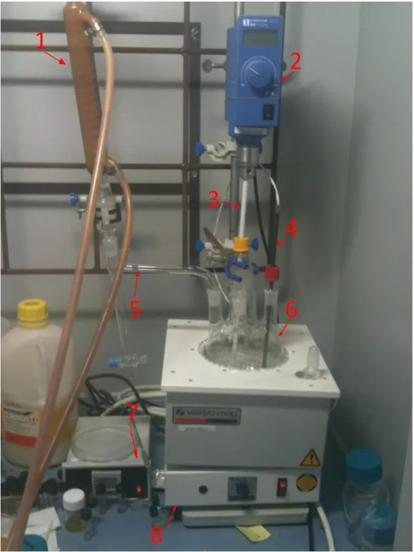
Synthesis of the encapsulation materials has been performed at UNAM laboratories. The setup used in our synthesis is presented seen in Figure 10. This setup enabled us in conducting repeatable synthesizes. In Figure 10, each number corresponds to a specific part of the system. Number 1 corresponds to the condenser. Condenser is the vital part of the system which enables refluxing. Refluxing is returning evaporated solvent back to the synthesis. Number 2 corresponds to the mixer engine. Mixer engine provides the power for mixing solvent during synthesis; it can be set to desired number of rotation per minute. Number 3 is the teflon mixer. Teflon mixer is rotated by the mixing engine and is resilient to heat and extreme acidic and basic environments. Number 4 is the thermocouple. Thermocouple is used with temperature controller (Number 7) to control the reaction temperature. Thermocouple measures the temperature of the solvent and transfers this information to temperature controller. Temperature controller controls the heater’s power supply. When the solvent is at a desired temperature, power of the heater is turned off. When temperature drops 1oC below the desired temperature, power is again supplied to the heater. Number 5 corresponds to the separator. Separator is used for collecting the condensed solvent. Number 6 is the flask. Flask is the glassware where reaction occurs. Number 8 is the heater. Heater is externally controlled by temperature controller to keep the flask at a required temperature.
34
35
Chapter 6
Parametrical Study and Results
Understanding the effects of different parameters on the properties of encapsulation material required a parametrical study. Parameters such as size of the nanoparticle, concentration of the nanoparticle, effect of different polymer formers, and effect of doping of ions have been investigated.
In this research work, three main parametrical studies have been conducted. First, a parametrical study was conducted to observe the effect of dopants on the film; second, a study was conducted to enhance the polymeric matrix; and last a study conducted to inspect the size effect.
Recipes explained in detail in Chapter 4 were used as an initial point. Syntheses for those recipes have been conducted. After the synthesis of the original recipe, a parameter was selected to be investigated to vary this parameter. Consecutive synthesizes were conducted with altered recipes. After synthesizes were completed, samples have been prepared on silicon wafers by using spin-coating method.
Measurements conducted on the prepared samples included; atomic force microscopy (AFM), scanning electron microscopy (SEM), ellipsometery, and contact angle characterization.
6.1 Effects of Various Polymer Formers
Various polymer formers are commercially available for use. To enhance loading capacity of polymer matrix, two polymer formers,
36
Aminopropyltriethoxysilane (APTES) and Vinyltrimethoxysilane (VTMO), have been used in our synthesis.
6.1.1 Effect of APTES on Encapsulation Material
Aminopropyltriethoxysilane (APTES) is a powerful adhesive additive, which is widely used by industry for enhancing binding between silica substrates and organic or metallic compounds [6.2*]. APTES have been investigated for both increasing the TiO2 loading of the encapsulation material and its adhesion to the
applied surface. A parametrical study to observe effects of APTES addition have been investigated. Samples with 1%, 3% and 5% APTES addition have been prepared and inspected. Refractive index results were combined with AFM results while comparing, morphological reasons have been understood. APTES addition has caused samples to have rough and uneven surfaces.
Figure 13. Effect of APTES concentration on refractive index.
Due to rough and uneven surface, refractive index results of the samples were not reproducible. In addition, as can be seen from Figure 13, increased APTES reduced the refractive index of the encapsulation material.
37
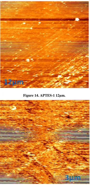
Figure 14. APTES-1 12µm.
Figure 15. APTES-1 3 µm.
The AFM results of the 1% APTES film can be seen in Figure 14 and 15, the film is nonuniform, although its roughness is higher than the 3% APTES film and lower than the rest.
38
Figure 16. APTES-2 12 µm.
Figure 17. APTES-2 3 µm
The AFM results of the 3% APTES film are presented in Figures 16 and 17, the film is more uniform when compared with the 1% sample. Although there are some major clusters on some parts, its roughness is relatively low when compared with other samples. The 3% samples were the only ones that produced repeatable results due to relatively low roughness.
39
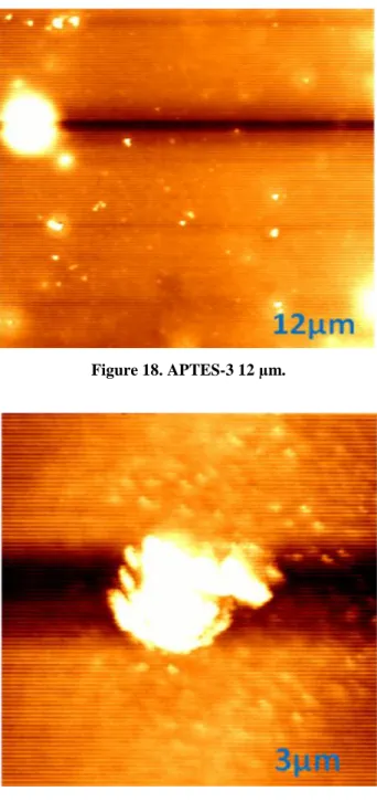
Figure 18. APTES-3 12 µm.
Figure 19. APTES-3 3 µm.
The AFM results of the 5% percent APTES films are shown in Figures 18 and 19. These results of this film were the worst case in terms of roughness and reproducible results compared to all other samples.
40
Figure 20. APTES-1 contact angle measurement showing hydrophobicity.
Figure 21. APTES-2 contact angle measurement showing hydrophobicity.
41
The presented data of contact angle measurements showed us that the hydrophobic property of encapsulation material has diminished with the addition of APTES. APTES disturbs the polymer matrix to prevent it from forming a hydrophobic surface.
6.1.2 Effects of VTMO on Encapsulation Material
Vinyltrimethoxysilane (VTMO) is an additive that hydrolyzes and forms methanol and reactive silanol (Si-OH) [6.1*]. VTMO addition was expected to enhance TiO2 loading due to its capability to bond inorganic substrates and react
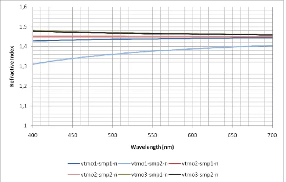
with each other to form (Si-O-Si) bonds. Parametrical studies for observing the effects of increasing VTMO have been conducted. In these studies VTMO-1, VTMO-2 and VTMO-3 stand for 1% VTMO addition, 3% VTMO addition and 5% VTMO addition in weight, respectively. Refractive index measurements of VTMO added samples were made to observe whether adding VTMO increases TiO2 amount in the material and therefore increases the refractive index.
42
As can be seen from Figure 23, the increasing amount of VTMO increased the refractive indices of the synthesized materials. Increased refractive index is expected because of the increase the TiO2 nanoparticles bonded in the polymer
matrix due to VTMO.
The VTMO’s effect on binding TiO2 nanoparticles into the polymer matrix can
also be observed with atomic force microscopy results. From AFM results, it can also be observed that the addition of VTMO into the synthesis also binds TiO2
particles to each other and forms larger TiO2 islands on the surface. This is not a
desired property because, instead of formation of TiO2 islands, it is preferred to
have them dispersed. Even TiO2 distribution would yield a coating material with
uniform properties.
43
Figure 25. VTMO-1 3 µm.
Figure 24 shows the general topography of the VTMO-1 coating. While having some TiO2 islands, there is also a fine dispersion of TiO2 particles on the
surface. Figure 25 shows a zoom in scan, which focuses on the surface clear of these large islands seen in Figure 24.
44
Figure 27. VTMO-2 3 µm.
Figure 26 gives a general topography of the VTMO-2 coating. When compared with VTMO-1, TiO2 isles are both larger and there are more of them. The fine
dispersion of TiO2 particles that appears on the surface of VTMO-1 also left
their place to minor TiO2 islands. Figure 27 is a zoom-in, which focuses on a
surface clear of large islands and focuses on minor ones.
45
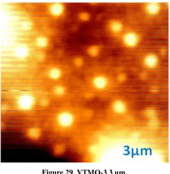
Figure 29. VTMO-3 3 µm.
Figure 28 depicts a topography scan of the VTMO-3 material coating. When compared with VTMO -1 and VTMO-2 TiO2 islands become even larger, and at
some points of the surface, it seems like they are merging together. As it seems, the fine dispersion of TiO2 particles on surface in VTMO-1, and the minor TiO2
isles of VTMO-2 are decreased in density, which leads to the opinion that those small islands are merged with big ones. Figure 29 at the bottom is a zoom-in which focuses on a surface clear of large islands and shows minor ones.
In addition to topographic and refractive index effects, VTMO also affects polymer chain. Fluoroalkylsilane used during synthesis was used to create a hydrophobic coating. Due to change in the polymer chain, it was necessary to investigate the effect of VTMO addition on the hydrophobicity.
46
Figure 30. VTMO-1 Contact angle measurement showing hydrophobicity.
Figure 31. VTMO-2 Contact angle measurement showing hydrophobicity.
47
As it can be seen from the figures above, there was no significant correlation between VTMO addition and hydrophobicity. The surfaces of all materials remained hydrophobic despite VTMO addition.
6.2 Effects of TiO
2Size and Concentration
TiO2 particles can be obtained in various diameters. In addition TiO2 can also be
synthesized in the form of rutile or anatese, which causes its various properties to differentiate. In this parametrical study, our aim is to use two different sizes of TiO2 in varying concentrations and evaluate their effects on material
properties. TiO2 of sizes 6 nm and 240 nm have been used in these studies. 6 nm
TiO2 was in anatese form and 240 nm TiO2 was rutile.
In order to evaluate Lévy effect on refractive index, samples with only 6 nm (small particle size, uniform light path), only 240 nm (big particle size, uniform light path) and combined (6 nm and 240 nm particles, Lévy behaviour) have been prepared. SEM and refractive index measurements were conducted.
6.2.1 Results of 6nm Samples
Following are the results of the samples prepared with 6 nm TiO2 particles. In
this parametrical study, the recipe to synthesize material with 6 nm TiO2 has
been altered to create under-loaded and over-loaded materials. In under-loading case, the amount of TiO2 was half of the original recipe, in over-loading case the
48
Figure 33. 6nm TiO2 particles, SEM measurement on 100 µm scale using under loaded
recipe.
49
Figure 35. 6 nm TiO2 Particles, SEM measurement on a 100 µm scale using overloaded
recipe.
After SEM measurements, we observed that during synthesis bond between TiO2 molecules are formed. In addition, it is observed that increasing the loading
of TiO2 causes more uniform films to be formed.
6.2.2 Results of 240 nm Samples
Following are the results of the samples prepared with 240 nm TiO2 particles. In
this parametrical study, the recipe to synthesize material with 240 nm TiO2 has
been altered to create loaded and over-loaded materials. In the under-loading case the amount of TiO2 was half of the original recipe, and in the
overloading case, the amount of TiO2 was twice of the original recipe, as in the
50
Figure 36. 240 nm TiO2 particles, SEM measurement on a 100 µm scale using under loaded
recipe.
51
Figure 38. 240 nm TiO2 particles, SEM measurement on a 100 µm scale using over-loaded
recipe.
SEM scanning results for 240 nm TiO2 particles turned in similar results with 6
nm particles. Bonding between TiO2 particles and better film uniformity with
increased TiO2 loading have been observed.
6.2.3 Results of 6 nm and 240 nm Combined Samples
Evaluating Lévy behavior required comparison of the combination of different sized particles with single sized particles. Following are the results of the samples prepared with both 6 nm and 240 nm TiO2 particles.
For the comparison, samples with six different combinations have been prepared for covering all possible scenarios. Samples are prepared as follows: under loaded (6 nm and 240 nm), original (6 nm and 240 nm), over loaded (6 nm and 240 nm), under loaded (6 nm) and over loaded (240 nm), over loaded (6 nm) and under loaded (240 nm), under loaded (6 nm) and original (240 nm), over
52
loaded (6 nm) and original (240 nm), original (6 nm) and under loaded (240 nm), original (6 nm) and over loaded (240 nm).
Figure 39. SEM measurement of under-loaded 6 nm and 240 nm sample (100 µm scale).
53
Figure 41. SEM measurement of over-loaded 6 nm and 240 nm sample (100 µm scale).
54
Figure 43. SEM of over-loaded 6 nm and under loaded 240 nm sample (100µm scale).
55
Figure 45. SEM of over-loaded 6 nm and original 240 nm sample (100µm scale).
56
Figure 47. SEM of original 6 nm and over-loaded 240 nm sample (100µm scale).
6.2.4 Results of refractive index measurements
SEM measurements provided information about film uniformity and morphology as well as TiO2 coverage on film surface. The information on film
uniformity is essential to understand refractive index results gathered by the ellipsometer measurements. Unfortunately the elliopsometer was not capable of providing reproducible results. This is attributed to narrow spot size of the ellipsometer. Therefore, it was decided to take data from a refractometer, which uses a larger area for taking data (on millimeter size). Refractive index measurements made with the refractometer resulted in repeatable data of refractive indices and thicknesses of the sample materials prepared. Since those measurements were not taken in an integrating sphere, the results may vary for strongly scattering complex media. The effect of TiO2 size and loading
57
Figure 48. Effect of concentration on the refractive index for 6 nm TiO2 particle.
Our first sample batch consists of synthesis made with 6 nm TiO2 particles with
varying concentrations. In refractive index results it has been observed that the medium recipe, which has the optimum concentration for TiO2 loading, had the
highest n values at all wavelengths. It is expected to have lower n values for lower concentration coating material, due to the reduced amount of TiO2
particles. It is normally expected to obtain higher n values for higher loading concentrations. However for 6 nm TiO2 particles, the higher TiO2 loading led to
a refractive index lower than all other conditions. This is possibly attributed to cluster formation of TiO2 particles at higher loading concentrations and
non-uniform TiO2 distribution. This is also supported by SEM images.
58
Figure 49. Effect of concentration on the refractive index for 240 nm TiO2 particle.
Our second sample batch consist of synthesis made with 240 nm TiO2 particles
with varying concentrations. In refractive index results it has been observed that highly TiO2 doped material yields the highest n values at all wavelengths, which
is an expected result. The trend of the SEM data also agrees with our expectations where that the medium concentration leads to lower n than those of the highly doping and the lower concentration, which give lower n values. The difference from the 6 nm sample trend might be related to the particle size. The weight percentage of TiO2 used in both synthesizes were the same, but there is a
40 times difference between their diamaeters, and therefore 1600 times difference in their surfaces and 64000 times difference in their volumes. High surface – volume ratio difference, which affects the cluster formation, might be the reason for the different trends. In small size particles, aggregation is much easier at high concentrations.
59
Figure 50. Effect of combining different sized TiO2 by using original recipe.
In Figure 50, to make use of Lévy glass, 6 nm and 240 nm particle samples have been combined. Their concentration was as in the medium doped recipe. It have been observed that 6 nm TiO2 doped material refractive index to be high, 240
nm TiO2 doped material to be low and combined material to be between other
materials.
To further investigate the Lévy glass, materials with low and high concentrated 6 nm and 240 nm TiO2 particles have been prepared. In low concentration case,
which can be observed in Figure 51, combined result was almost the same with low doped 240 nm, while 6 nm TiO2 material was higher as in the case of
original recipe.
60
Figure 51. Effect of combining different sized TiO2 on low concentration.
In the high loading case, we observed that the refractive index exhibit a similar behaviour in the combo sample. Different than other samples, in the high loading case, the refractive index of the 240 nm sample was higher than 6 nm sample. That was due to aggregation of the 6 nm particles, which caused the samples to have lower refractive index than the 240 nm sample.
In Figure 53, the effect of loading in the combined samples on the refractive index have been investigated. The refractive index of the low loading case was the lowest, which was expected due to low amount of TiO2 particles. High
loading condition leads to a refractive index higher than the low condition due to high TiO2 loading but it was still lower than the medium loading condition. High
loading case has aggregation of 6 nm particles, which has decreased refractive index. Therefore, the medium loading condition was optimum for combo samples.
61
Figure 52. Effect of combining different sized TiO2 in high concentration.
Figure 53. Effect of concentration on refractive index of combo materials.
(nm)
62
6.2.4 Results of transparency and absorption
measurements
Transparency measurements conducted to evaluate transparency of the encapsulation materials prepared. High transparency is expected from encapsulation materials.
Figure 54. Absorption results for 6 nm particle samples.
6 nm particle samples demonstrated expected results, as the nanoparticle loading of the samples increased the absorption of the samples increased as well. For the high loading case where SEM results show aggregation absorption was severe.
In 240 nm particles similar behavior observed. There was no dramatic increase in absorbance due to fact that there are no aggregations. Absorption was lower than 6 nm particle cases in general due to fact that there are less absorption centers within the composite material.
63
Figure 55. Absorption results for 240 nm particle samples.
Transparency results of samples are coherent with the absorption results. For 6 nm particles transparency is between 90%-75% which is good for an encapsulation material. For aggregated 6 nm sample transparency is low but still above 50%.
In 240 nm particle case, transparency is higher than 6 nm case due to less absorption, which is result of lower number of absorption centers. Transparency of 240 nm particles are above 90% in best case and doesn’t drop below 75% under the worst case.
Overall, materials developed have good transparency values to be fit as encapsulation materials.
64
Figure 56. Transparency results for 6 nm particle samples.
65
Chapter 7
Conclusions
During this thesis research work several coating materials have been synthesized by using sol-gel technique and analyzed by using various characterization approaches. A set of parametrical studies were conducted by repeating recipes with varying parameters. Studies conducted can be divided into two major categories: enhancing the polymer matrix, and evaluating the effect of the size of the semiconductor dopants to films.
First, the effect of the boron doping on TiO2 embedded silica films have been
studied. In the parametrical study conducted to evaluate silica films, four types of samples were prepared. Prepared samples included TiO2 and boron combined,
only boron, only TiO2, and neither of the dopants. Our expectations were to
observe enhancements in various properties of boron and TiO2 combined films
when compared with others. AFM measurements of the films showed significant topographical patterns in only TiO2 consisting films. There was no pattern in
non-TiO2 films and the pattern in TiO2 only film was diminished when boron
was added. Contact angle measurement results showed us fluoroalkylsilane is dominant on providing hydrophobicity to films.
In the second phase of the research work APTES and VTMO compounds were introduced to the synthesis and their effects were observed. The purpose of using those polymer formers was to obtain better surface topography and increase the content of the TiO2 in the films. Increased TiO2 content was desired
to increase the refractive index of the material synthesized. Materials synthesized with APTES formed nonuniform surfaces. In addition to nonuniformity there was no increase in TiO2 content of the films. Those
66
In addition to those negative results, APTES also suppressed hydrophobicity provided by fluoroalkylsilane. Therefore, APTES added films were not hydrophobic. On contrary, samples prepared with VTMO increased TiO2 content
of the films they were added. In addition, the surface of the film was also uniform. Results obtained from VTMO samples were reproducible and there was an increasing refractive index trend. Although observation with AFM showed that, with increasing VTMO, there was also an increase in TiO2
aggregation. This aggregation prevented us from forming uniform film, due to limited TiO2 distribution. It must be also noted that VTMO addition, unlike
APTES, did not suppress the hydrophobicity of films. These results show that, for the intention of this research, VTMO is more beneficial than APTES.
In the third phase, the effects of particle size and combination on refractive index and film properties were investigated. 6 nm and 240 nm TiO2 particles
were used. The effect of different loading percentages was also studied. Lévy glass approach was pursued by preparing samples with different concentrations of different sized nanoparticles. SEM, ellipsometer, refractometer and absorption measurements were taken on these samples. SEM measurements showed that as the TiO2 amount is increased, particles distributed in the material
is more uniformly. Ellipsometer measurements did not provide repeatable results, despite observing uniform films in SEM. The ellipsometer’s spot size was too small and, therefore, yielded different results on the same films. After failing to obtain reliable data using ellipsometer, a refractometer was used. The refractometer scans larger area to obtain data. Therefore, it is less effected by nonuniformity and provides more reliable results. The refractometer results show that the films were in similar thicknesses (between 45 and 65 nm). The absorbtion data show that the films exhibit optical transparency varies between 75% and 90%.
In this thesis work, three different ideas were pursued. Synthesizes, parametrical study and various measurements were conducted and results were compared.
![Figure 3. Position of encapsulation material within the LED [27]](https://thumb-eu.123doks.com/thumbv2/9libnet/5912811.122560/17.892.272.697.183.533/figure-position-encapsulation-material-led.webp)
![Figure 6. Transparency change of silicone under exposure to 200 o C for various time intervals [28]](https://thumb-eu.123doks.com/thumbv2/9libnet/5912811.122560/21.892.195.772.264.528/figure-transparency-change-silicone-exposure-various-time-intervals.webp)
![Figure 7. Effect of temperature on lifetime of LEDs [37].](https://thumb-eu.123doks.com/thumbv2/9libnet/5912811.122560/26.892.203.762.447.722/figure-effect-temperature-lifetime-leds.webp)